
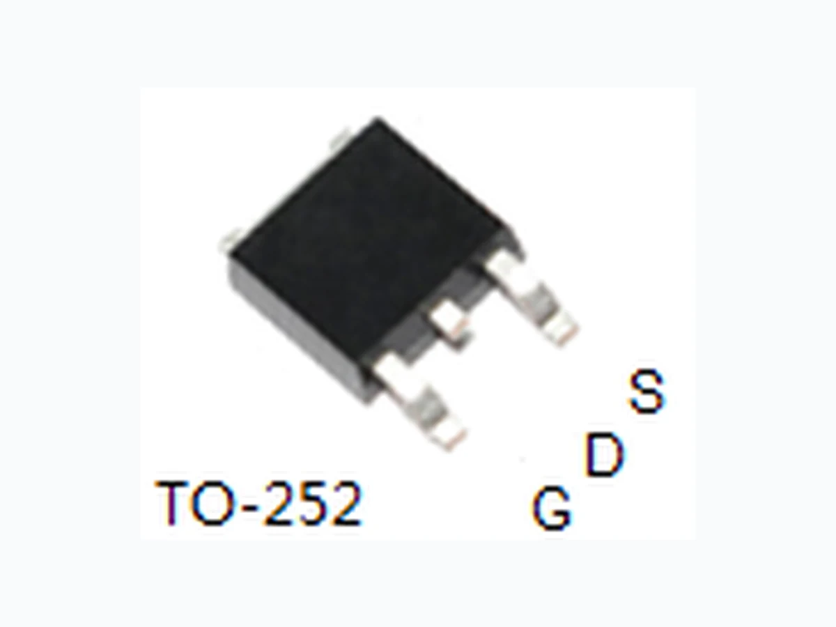
LM8N25D LEIDITECH
Document overview
- Manufacturer or author: Provided By www.digicamel.com(FREE DATASHEET DOWNLOAD SITE)
- PDF pages: 9
Technical content
FEATURES
Fast switching 100% avalanche tested Improved dv/dt capability
APPLICATIONS
Switch Mode Power Supply (SMPS) Uninterruptible Power Supply (UPS) Power Factor Correction (PFC) Device Marking and Package Information Device Package Marking LM8N25F TO-220F LM8N25P TO-220 LM8N25U TO-251 LM8N25D TO-252 Absolute Maximum Ratings TC = 25º C,unless otherwise noted Parameter Symbol Value Unit TO-220F TO-220 TO-251 TO-252 Drain-Source Voltage (VGS = 0V) VDSS 250 V Continuous Drain Current ID 8 A Pulsed Drain Current (note1) IDM 32 A Gate-Source Voltage VGSS ±30 V Single Pulse Avalanche Energy (note2) EAS 218 mJ Avalanche Current (note1) IAS 6.6 A Repetitive Avalanche Energy (note1) EAR 130 mJ Power Dissipation (TC = 25º C) PD 54 83 W Operating Junction and Storage Temperature Range TJ, Tstg -55~+150 ºC Thermal Resistance Parameter Symbol Value Unit TO-220F TO-251 TO-252 TO-220 Thermal Resistance, Junction-to-Case RthJC 2.3 1.5 K/W Thermal Resistance, Junction-to-Ambient RthJA 62.5 60 LM8N25D Enhancement Mode Power MOSFET N-Channel Rev : www.leiditech.com 01.06.2018 1/9
Specifications TJ = 25ºC, unless otherwise noted Parameter Symbol Test Conditions Value Unit Min. Typ. Max. Static Drain-Source Breakdown Voltage V(BR)DSS VGS = 0V, ID = 250µ A 250 -- -- V Zero Gate Voltage Drain Current IDSS VDS = 250V, VGS = 0V, TJ = 25º C -- -- 1 μA Gate-Source Leakage IGSS VGS = ±30V -- -- ±100 nA Gate-Source Threshold Voltage VGS(th) VDS = VGS, ID = 250µ A 2 -- 4 V Drain-Source On-Resistance (Note3) RDS(on) VGS = 10V, ID = 4.0A -- 0.45 0.52 Ω Dynamic Input Capacitance Ciss VGS = 0V, VDS = 25V, f = 1.0MHz -- 467 -- pFOutput Capacitance Coss -- 79 -- Reverse Transfer Capacitance Crss -- 39 -- Total Gate Charge Qg VDD = 200V, ID = 8.0A, VGS = 10V -- 31 -- nCGate-Source Charge Qgs -- 1.5 -- Gate-Drain Charge Qgd -- 15 -- Turn-on Delay Time td(on) VDD = 125V, ID =8.0A, RG = 25 Ω -- 34 -- ns Turn-on Rise Time tr -- 8 -- Turn-off Delay Time td(off) -- 185 -- Turn-off Fall Time tf -- 53 -- Drain-Source Body Diode Characteristics Continuous Body Diode Current IS TC = 25 º C -- -- 8 A Pulsed Diode Forward Current ISM -- -- 32 Body Diode Voltage VSD TJ = 25º C, ISD = 4.0A, VGS = 0V -- -- 1.4 V Reverse Recovery Time trr VGS = 0V,IS = 8.0A, diF/dt =100A /μs -- 158 -- ns Reverse Recovery Charge Qrr -- 0.8 -- μC Notes 1. Repetitive Rating: Pulse width limited by maximum junction temperature 2. L = 10mH, VDD = 30V, RG = 25 Ω, Starting TJ = 25 ºC 3. Pulse Test: Pulse width ≤ 300μs, Duty Cycle ≤ 1% LM8N25D Rev : www.leiditech.com 01.06.2018 2/9
Figure A:Gate Charge Test Circuit and Waveform Figure B:Resistive Switching Test Circuit and Waveform Figure C:Unclamped Inductive Switching Test Circuit and Waveform LM8N25D Rev : www.leiditech.com 01.06.2018 5/9
Rev : www.leiditech.com 01.06.2018 6/9
Rev : www.leiditech.com 01.06.2018 7/9
Rev : www.leiditech.com 01.06.2018 8/9
Shanghai Leiditech Electronic Co.,Ltd Email: sale1@leiditech.com Tel : +86- 021 50828806 Fax : +86- 021 50477059 Rev : www.leiditech.com 01.06.2018 9/9