
LM857N5 LEIDITECH
Document overview
- Manufacturer or author: Provided By www.digicamel.com(FREE DATASHEET DOWNLOAD SITE)
- PDF pages: 3
Technical content
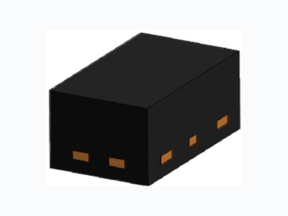
General Purpose Transistor PNP Silicon Surface Mount Plastic Package Absolute Maximum Ratings (TA = 25°C unless otherwise noted) Symbol Parameter Value Units VCBO Collector-Base Voltage -40 V VCEO Collector-Emitter Voltage -40 V VEBO Emitter-Base Voltage -5 V IC Collector Current -200 mA PD Power Dissipation (FR-4 Board – minimum pad) 200 mW RθJA Thermal Resistance from Junction to Ambient 600 °C /W TJ TSTG Junction & Storage Temperature Range -55 to +150 °C These ratings are limiting values above which the serviceability of the device may be impaired. Specification Features: § DFN1006-3 § Simplifies Circuit Design § RoHS Compliant § Green EMC § Matte Tin(Sn) Lead Finish § Weight: approx. 0.001g Electrical Symbol: Device Marking Code: Device Type Marking Shipping 10,000/Reel Electrical Characteristics (TA = 25°C unless otherwise noted) Off Characteristics Symbol Parameter Test Condition Limits Unit Min Max V(BR)CEO Collector-Emitter Breakdown Voltage (Note 1) IC =-1mA, IB =0A -40 - Volts V(BR)CBO Collector-Base Breakdown Voltage IC =-10uA, IE =0A -40 - Volts V(BR)EBO Emitter-Base Breakdown Voltage IE =-10uA, IB =0A -5 - Volts ICEX Collector Cutoff Current VCE =-30V, VEB =-3V - -50 nA IEBO Emitter Cutoff Current VEB=-5V, IC=0A -100 nA Note 1: Pulse Test. Pulse width <300us, Duty cycle < 2.0%. Green Product DFN1006-3 1 2 LM857BN5 LM857N5 Rev 2.0 : www.leiditech.com 12.01.2019 1/3 DFN1006-3DFN1006-3DFN1006-3DFN1006-3DFN1006-3DFN1006-3DFN1006-3DFN1006-3
On Characteristics (Note 1) Symbol Parameter Test Condition Limits Unit Min Max HFE DC Current Dain IC =-0.1mA, VCE =-1V IC =-1.0mA, VCE =-1V IC =-10mA, VCE =-1V IC =-50mA, VCE =-1V IC =-100mA, VCE =-1V 100 300 VCE(sat) Collector-Emitter Saturation Voltage IC=-10mA, IB=-1mA IC=-50mA, IB=-5mA -0.25 -0.4 Volts VBE(sat) Base-Emitter Saturation Voltage IC=-10mA, IB=-1mA IC=-50mA, IB=-5mA -0.65 -0.85 -0.95 Volts Small-signal Characteristics Symbol Parameter Test Condition Limits Unit Min Max fT Current-Gain-Bandwidth Product IC =-10mA, VCE =-20V, f = 100MHz 250 - MHz Cobo Output Capacitance VCB =-5V, IE =0A, f = 1.0MHz - 4.5 pF Cibo Input Capacitance VBE =-0.5V, IC =0A, f = 1.0MHz - 10 pF hie Input Impedancen VCE =-10V, IC =-1mA, f = 1.0kHz 2 12 pF hre Voltage Feedback Ratio VCE =-10V, IC =-1mA, f = 1.0kHz 0.1 10 X10-4 hfe Small-signal Current Gain VCE =-10V, IC =-1mA, f = 1.0kHz 100 400 - hoe Output Admittance VCE =-10V, IC =-1mA, f = 1.0kHz 3 60 θmhos NF Noise Figure VCE =-5V, IC =-100uA Rs=1.0kΩ f = 1.0kHz 4 dB Switching Characteristics Symbol Parameter Test Condition Limits Unit Min Max td tr Delay Time Rise Time VCC =-3V, VBE =-0.5V, IC =-10mA, IB1 =-1mA nS ts tf Storage Time Fall Time VCC =-3V, IC =-10mA, IB1 = IB2 =-1mA 225 nS LM857N5 Rev 2.0 : www.leiditech.com 12.01.2019 2/3
Typical Soldering Pattern(mm): DIM MILLIMETERS INCHES MIN MAX MIN MAX A 0.46 0.50 0.018 0.020 D 0.55 0.65 0.022 0.026 E 0.95 1.05 0.037 0.041 b 0.12 0.22 0.005 0.008 b1 0.45 0.55 0.018 0.022 L 0.22 0.32 0.008 0.013 L1 0.22 0.32 0.008 0.013 e Typ. 0.34 Typ. 0.013 e1 Typ. 0.65 Typ. 0.026 LM857N5 Shanghai Leiditech Electronic Co.,Ltd Email: sale1@leiditech.com Tel : +86- 021 50828806 Fax : +86- 021 50477059 Rev 2.0 : www.leiditech.com 12.01.2019 3/3