
LM6911 LEIDITECH
Document overview
- Manufacturer or author: Provided By www.digicamel.com(FREE DATASHEET DOWNLOAD SITE)
- PDF pages: 5
Technical content
Features
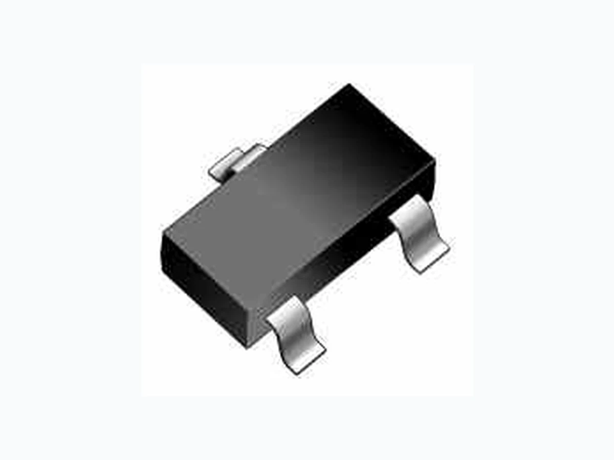
ID (at VGS=-10V) RDS(ON) (at VGS=-10V) -60V -2A 190mΩ(Max) Absolute Maximum Ratings TA=25°C unless otherwise noted Parameter Symbol Maximum Units Drain-Source Voltage VDS -60 V Gate-Source Voltage VGS ±20 V Drain Current-Continuous TC=25°C ID A TC=100°C ID -1.25 A Maximum Power Dissipation PD 1.56 W Junction and Storage Temperature Range TJ,TSTG -55 To 150 ℃ Thermal Characteristics Parameter Symbol Typ Max Unit Thermal Resistance junction-case RθJc 1.1 ℃ /W Thermal Resistance junction-to-Ambient RθJA ℃ /W D G S D G S SOT23 I DM Drain Current – Pulsed --8 A LM6911 Rev 2.0 : www.leiditech.com 12.01.2019 1/5
Electrical Characteristics (TJ=25℃ unless otherwise noted) Symbol Parameter Condition Min Typ Max Unit STATIC PARAMETERS BVDSS Drain-Source Breakdown Voltage VGS=0V ID=-250μA -60 V IDSS Zero Gate Voltage Drain Current VDS=-60V,VGS=0V 1 μA IGSS Gate-Body Leakage Current VGS=±20V,VDS=0V ±100 nA VGS(th) Gate Threshold Voltage VDS=VGS,ID=-250μA -1.0 -1.6 -2.5 V RDS(ON) Drain-Source On-State Resistance VGS=-10V, ID=-2A 160 190 mΩ VGS=-4.5V, ID=-1.5A 200 240 mΩ DYNAMIC PARAMETERS Clss Input Capacitance VDS=-30V,VGS=0V , F=1.0MHz 426 pF Coss Output Capacitance pF Crss Reverse Transfer Capacitance pF SWITCHING PARAMETERS td(on) Turn-on Delay Time VDS=-30V,ID=-1A , VGS=-10V, RG=6Ω 5.2 nS tr Turn-on Rise Time nS td(off) Turn-Off Delay Time nS tf Turn-Off Fall Time 10.6 nS Qg Total Gate Charge VDS=-30V,ID=-3A , VGS=-10V 5.2 nC Qgs Gate-Source Charge nC Qgd Gate-Drain Charge nC VSD Diode Forward Voltage VGS=0V,ISD=-1A 0.72 1.4 V Note: 1. Repetitive Rating : Pulsed width limited by maximum junction temperature. 2. The data tested by pulsed , pulse width≦ 300us , duty cycle≦ 2%. 3. Essentially independent of operating temperature. LM6911 Rev 2.0 : www.leiditech.com 12.01.2019 2/5
TYPICAL ELECTRICAL AND THERMAL CHARACTERISTICS TC , Case Temperature (℃) Fig.1 Continuous Dr ain Current vs. TC Normalized On Resistance (mΩ) TJ , Junction Temperature (℃) Fig.2 Normalized RDSON vs. TJ TJ , Junction Temperature (℃) Fig.3 Normalized Vth vs. TJ GS Gate to Source Voltage (V) Qg , Gate Charge (nC) Fig.4 Gate Charge W aveform Normalized Thermal Response (R θJC Square Wave Pulse Duration (s) Fig.5 Normalized Transient Impedance D Continuous Drain Current (A) -VDS , Drain to Source Voltage (V) Fig.6 Maximum Safe Operation Area D , Continuous Drain Current (A)Normalized Gate Threshold V oltage (V) LM6911 Rev 2.0 : www.leiditech.com 12.01.2019 3/5
TYPICAL ELECTRICAL AND THERMAL CHARACTERISTICS T d(on) T r T on T d(off) T f T off V DS V GS 90% 10% Fig.7 Switching Time Waveform Fig.8 EAS Waveform LM6911 Rev 2.0 : www.leiditech.com 12.01.2019 4/5
Symbol Dimensions In Millimeters Dimensions In Inches Min Max Min Max A 0.900 1.000 0.035 0.039 A1 0.000 0.100 0.000 0.004 b 0.300 0.500 0.012 0.020 c 0.090 0.110 0.003 0.004 D 2.800 3.000 0.110 0.118 E 1.200 1.400 0.047 0.055 E1 2.250 2.550 0.089 0.100 e 0.950 TYP. 0.037 TYP. e1 1.800 2.000 0.071 0.079 L 0.550 REF. 0.022 REF. L1 0.300 0.500 0.012 0.020 θ 1° 7° 1° 7° SOT23 PACKAGE INFORMATION LM6911 Shanghai Leiditech Electronic Co.,Ltd Email: sale1@leiditech.com Tel : +86- 021 50828806 Fax : +86- 021 50477059 Rev 2.0 : www.leiditech.com 12.01.2019 5/5