
DATASHEET SEARCH SITE
Document overview
- Manufacturer or author: Provided By www.digicamel.com(FREE DATASHEET DOWNLOAD SITE)
- PDF pages: 4
Technical content
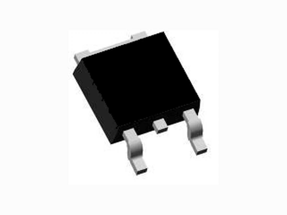
Main Product Characteristics: Features and Benefits: Description: Absolute max Rating: Symbol Parameter Max. Units ID @ TC = 25°C Continuous Drain Current, VGS @ 10V① -60 A ID @ TC = 100°C Continuous Drain Current, VGS @ 10V① -50 IDM Pulsed Drain Current② -240 ISM Pulsed Source Current (Body Diode)② -240 PD @TC = 25°C Power Dissipation③ 166 W VDS Drain-Source Voltage -60 V VGS Gate-to-Source Voltage ± 20 V EAS Single Pulse Avalanche Energy @ L=0.3mH 300 mJ IAS Single Pulse Avalanche Current @ L=0.3mH 44 A TJ TSTG Operating Junction and Storage Temperature Range -55 to + 150 °C VDSS -60V RDS(on) 12mΩ (typ.) ID -60A TO-252 Schematic diagram Advanced trench MOSFET process technology Special designed for PWM, load switching and general purpose applications Ultra low on-resistance with low gate charge High Power and current handing capability Fully Avalanche Rated It utilizes the advanced trench processing techniques to achieve extremely low on resistance and low gate charge. These features combine to make this design an extremely efficient and reliable device for use in PWM, load switching and a wide variety of other applications. D G S Enhancement Mode Fieid Effect Transistor P-Channel LM6025D Rev 2.0 : www.leiditech.com 12.01.2019 1/4 D G S
Symbol Characterizes Value Unit RθJA Junction-to-ambient (t ≤ 10s) ④ 62 ℃/W RJC Maximum Junction-to-Case⑤ 0.75 ℃/W Electrical Characterizes @TA=25℃ unless otherwise specified Symbol Parameter Min. Typ. Max. Units Conditions BVDSS Drain-to-Source breakdown voltage -60 — — V VGS = 0V, ID =- 250μA RDS(on) Static Drain-to-Source on-resistance — 12 25 mΩ VGS=-10V, ID =- 23A TJ = 125℃ — 22 — VGS(th) Gate threshold voltage -1 -3 V VDS = VGS, ID =-250uA IDSS Drain-to-Source leakage current — — -1 μA VDS =-60V,VGS = 0V — — -50 TJ = 125°C IGSS Gate-to-Source forward leakage — — 100 nA VGS =20V Gate-to-Source reverse leakage — — -100 VGS = -20V Qg Total gate charge — — 170 nC ID=-30A, VDD=-40V, VGS=-10V Qgs Gate-to-Source charge — — 30 Qgd Gate-to-Drain("Miller") charge — — 70 td(on) Turn-on delay time — 15.2 — ns VDD=-30V,ID=-20A, RL=1.50Ω,RG=3.00Ω, VGS=-10V tr Rise time — 23.7 — td(off) Turn-Off delay time — 53.3 — tf Fall time — 12.7 — Ciss Input capacitance — 7456 — pF VDS=-25V, VGS=0V, f=1MHZ Coss Output capacitance — 376 — Crss Reverse transfer capacitance — 293 — Source-Drain Ratings and Characteristics Symbol Parameter Min. Typ. Max. Units Conditions IS Maximum Body-Diode Continuous Current — -60 — A MOSFET symbol showing the integral reverse p-n junction diode. ISM Maximum Body-Diode Pulse Current — -240 — A VSD Diode Forward Voltage — -0.74 -1.2 V TJC,IS=-10A,VGS=0V trr Reverse Recovery Time — 38.2 — nS TJ = 25℃, IF =-20A, di/dt = 100A/μs Qrr Reverse Recovery Charge — 62.5 — nC D G S LM6025D Rev 2.0 : www.leiditech.com 12.01.2019 2/4
Test circuits and Wave forms EAS Test Circuit: Gate charge test circuit: Switching Time Test Circuit: Switching Waveforms: Notes: ①Calculated continuous current based on maximum allowable junction temperature. ②Repetitive rating; pulse width limited by max. junction temperature. ③The power dissipation PD is based on max. junction temperature, using junction-to-case thermal resistance. ④The value of RθJA is measured with the device mounted on 1 in 2 FR-4 board with 2oz. Copper, in a still air environment with TA =25°C LM6025D Rev 2.0 : www.leiditech.com 12.01.2019 3/4
K 5.350 (REF) 2.900 (REF) 1.600 (REF) 80 (REF) 80 (REF) 0.063 (REF) 0.211 (REF) 0.114 (REF) Symbol Dimension In Millimeters Dimension In Inches 4.83 (REF) 0.190 (REF) LM6025D ■ T Shanghai L eiditech Electronic Co.,Ltd Email: sale1@leiditech.com Tel : +86- 021 50828806 Fax : +86- 021 50477059 Rev 2.0 : www.leiditech.com 12.01.2019 4/4