
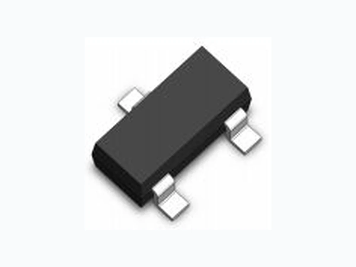
LM6002 LEIDITECH
Document overview
- Manufacturer or author: Provided By www.digicamel.com(FREE DATASHEET DOWNLOAD SITE)
- PDF pages: 5
Technical content
Description
Rev : www.leiditech.com N-Channel M O S F E T LM6002 D(3) S(2) G(1) The MOSFET provide the best combination of fast switching, low on-resistance and cost-effectiveness. MOSFET Product Summary V DS (V) R DS(on) (Ω) I D (A) 100 0.23@ VGS=10V 2 Parameter Symbol Value Units Drain-Source Voltage V DS 100 V Gate-Source Voltage V GS ±20 V Continuous Drain Curren T A =25℃ I D A T A =70℃ 0.8 Pulsed Drain Current I DM A Avalanche Current I AS 18 A Avalanche Energy L=0.1mH EAS 16.5 mJ Maximum Power Dissipation T A =25℃ P D 0.75 W T A =70℃ 0.3 Operating Junction and Storage Temperature Range T T STG -55 to 150 Thermal Resistance-Junction to Ambient R θJA 166 ℃/W Absolute maximum rating@25℃ 01.06.2014
Rev : www.leiditech.com Parameter Symbol Conditions Min. Typ. Max. Units OFF/ON CHARACTERISTICS STATIC PARAMETERS Drain-Source Breakdown Voltage BV DSS I D =250μA,V GS =0V 100 - V Zero Gate Voltage Drain Current I DSS V DS =80V,V GS =0V μA V DS =80V,V GS =0V T J =1255℃ Gate-Body Leakage I GSS V DS =0V,V GS =±20V - - ±100 nA Gate Threshold Voltage V GS(th) V DS GS , I D =250μA 1.0 1.5 2.0 V On-State Drain Current I D(ON) V DS = 10V, V GS = 10V 18 A Drain-Source On- Static Resistance R DS(ON) V GS =10V, I D =2A 0.2 0.23 Ω V GS =5V, I D =1A 0.22 0.25 Ω Forward Transconductance g fs V DS = 10V, I D = 2A 10 S DYNAMIC PARAMETERS Input Capacitance C ISS V GS =0V, V DS =25V, f=1MHz 800 pF Output Capacitance C OSS pF Reverse Transfer Capacitance C RSS pF Gate Resistance R g V GS = 0V, V DS = 0V, f = 1MHz 2.5 Ω Total Gate Charge Q g V DS = 50V, V GS = 10V, I D nC Gate-Source Charge Q gs Gate-Drain Charge Q gD Electrical characteristics per line@25℃( unless otherwise specified) Turn-On Delay Time t d(on) V DD = 50V,I D @ 2A, V GS 10V, R GS = 6Ω nS Rise Time t r 330 Turn-Off Delay Time t d(off) Fall Time t f 111 SOURCE-DRAIN DIODE RATINGS AND CHA RACTERISTICE ( TJ = 25 °C ) Continuous Current I S A Forward Voltage1 V SD I F = 2A, V GS = 0V 1.4 V Reverse Recovery Time t rr I F = 2A, dl/dt = 500A/µS nS Reverse Recovery Charge Q rr 0.17 nC 01.06.2014 LM6002
Rev : www.leiditech.com 01.06.2014 LM6002
Rev : www.leiditech.com 01.06.2014 LM6002
Shanghai Leiditech Electronic Co.,Ltd Email: sale1@leiditech.com Tel : +86- 021 50828806 Fax : +86- 021 50477059 Millimeters Inches Symbol Min. Nom. Max. Min. Nom. Max. 0.01 0.06 0.10 0.001 0.002 0.004 c 0.09 0.13 0.18 0.003 0.005 0.007 E 1.20 1.30 1.40 0.047 0.051 0.055 L 0.35 0.54 0.69 0.014 0.021 0.029 Symbol Millimeters Inches X 0.80 0.031 0.95 0.037 Y 0.90 0.035 Z 2.00 0.079 Soldering Footprint Rev : www.leiditech.com 01.06.2014 LM6002