
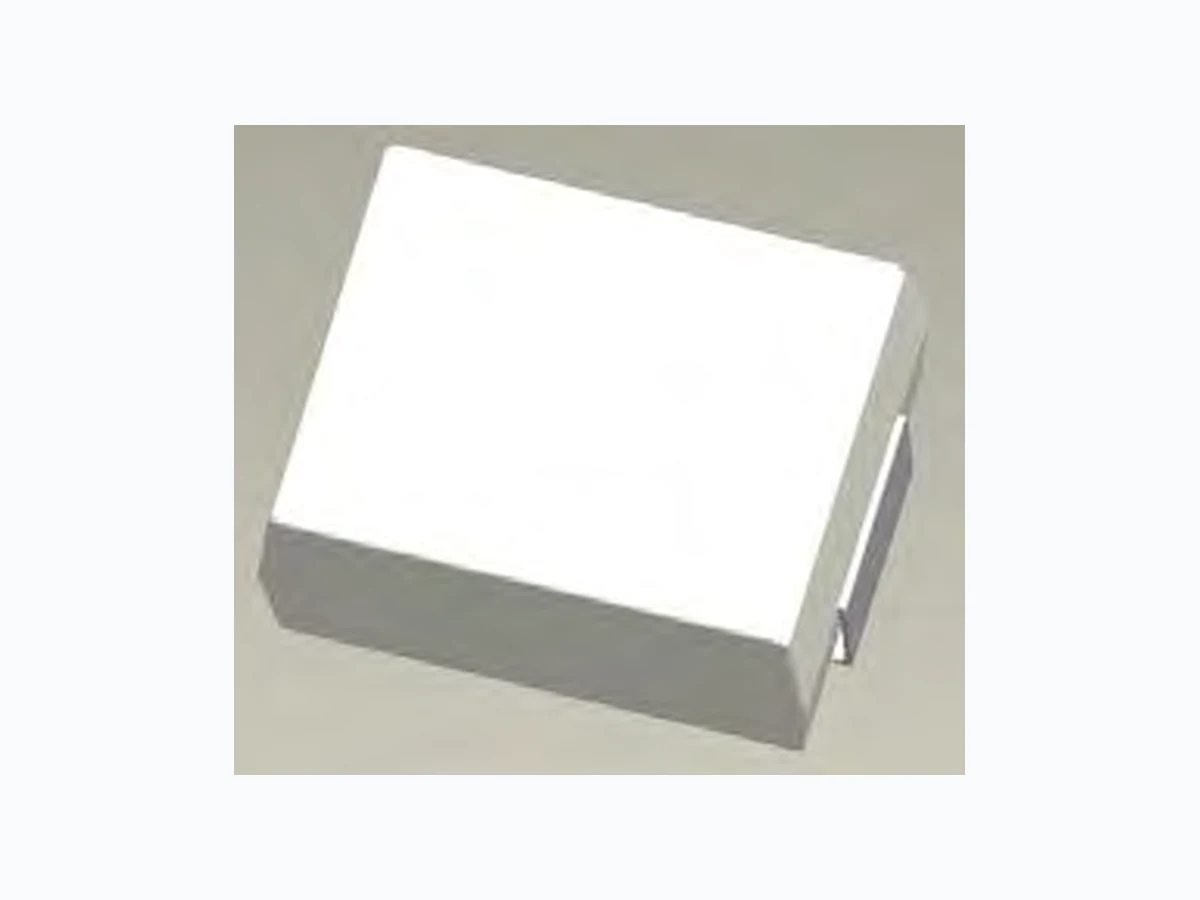
LDT4032 LEIDITECH
Document overview
- Manufacturer or author: Provided By www.digicamel.com(FREE DATASHEET DOWNLOAD SITE)
- PDF pages: 7
Technical content
FEATURES
Improved component design in a compact case High surge current capability of up to 3.5 kA Superior performance at high temperature White package design without shadow in LED lighting application SMD mountable disk varistors, suitable for lead-free reflow / wave soldering
APPLICATIONS
Power supplies for telecommunication systems Protection for LED circuits Protection for consumer, industrial equipment P rotection for automotive electronics APPLICABLE STANDARDS UL1449 IEC61051-1, -2, -2-2, IEC60950-1 Annex Q GB/T10193, GB/T10194, GB4943.1, GB8898 IEC61000-4-5 TYPE CODE DESIGNATION LDT 4032 - 471 H Varistor voltage V1mA: 47×10 =470 V Tolerance of varistor voltage at 1 mA: ±10%(V 1mA GENERALTECHNICALDATA Parameter Value Unit Operating temperature -55 to +125 ℃ Storage temperature -55 to +150 ℃ Electric strength 2.5 kV RMS Insulation resistance 100 MΩ Leiditech: logo High absorption SMD Disc Varisttors LDT4032 Series Rev 2.0 : www.leiditech.com 12.01.2019 1/7
a=125℃) SM D Types IA Case 40×32 in inch) Cont inuous Voltage Peak Current (8/ 20 μs) Ener gy ms) Rat ed Power Max Ma x Max VRMS VDC (1 ti me) (2 times) (1 time) [V] [V] [A] [A] [J] [mW] LDT 4032 - 271H 175 225 2500 1500 400 LDT 4032 - 391H 250 320 2500 1500 50 400 LDT 4032 - 431H 275 350 2500 1500 55 400 LDT 4032 - 471H 300 385 2500 1500 60 400 LDT 4032 - 511H 320 420 2500 1500 67 400 LDT 4032 - 561H 350 460 2500 1500 67 400 LDT 4032 - 621H 385 505 2500 1500 67 400 LDT 4032 - 681H 420 560 2500 1500 67 400 LDT 4032 a=25℃) SM D Types IA Case 40×32 in inch) Varistor Voltage at 1 mA Clamping Voltage at Class Current (8/20 μs) Class Current (8/20 μs) Capacitance Max (±1 0%) (at 1 kHz) [V] [V] [A] [pF] LDT 4032 - 271H 270 455 25 350 LDT 4032 - 391H 390 650 25 300 LDT 4032 - 431H 430 710 25 270 LDT 4032 - 471H 470 775 25 230 LDT 4032 - 511H 510 845 25 210 LDT 4032 - 561H 560 930 25 200 - 681 H 680 1120 25 170 LDT4032 Series Rev 2.0 : www.leiditech.com 12.01.2019 2/7
e usage of mild, non-activated fluxes for soldering is recommended, as well as proper cleaning of the PCB. The components are suitable for reflow soldering per JEDEC J-STD-020C. - Wav e soldering Temper ature 250 300 Ti me 2K/s 0 50 100 150 200 s 250 100 150 200 100℃~130℃ 235℃~260℃ appr ox. 200K/s 1st wave 2nd w ave 5K/s 2K/s Forced cooling Normal c urve Limit curve s Te mperature characteristics at component terminal with dual-wave soldering LDT4032 Series Rev 2.0 : www.leiditech.com 12.01.2019 3/7
- Re flow soldering Tem perature TS(m in) TS( max) TL TP tp tL time t o peak temperatue Time 25 ℃ to pea k) Ramp-up Ramp-down Preheat Critical Zone TL to TP ts Pr ofile feature Sn-Pb assembly Pb-Free assembly Av erage ramp-up rate (TSma x to Tp) 3℃/se c. Max 3℃/sec. Max Pr eheat -Temperature min. (Ts(m in)) +100℃ +150 -Te mperature max.(Ts( max)) +150℃ +200 -Ti me (tSm in to tSma x) 60-120 secs. 60-180 secs. Ts(m ax) to TL - Ram p-up Rate 3℃/sec. Max 3℃/sec. Max Ti me maintained above -Temperature min. (TL) +183℃ +217 -Time (tL) 60-15 0 secs. 60-150 secs. Pe ak classification temperature (Tp) +220 Tim e within 5℃of actual peak temperature (tp) 10 secs. to 30 secs. 20 secs. to 40 secs. Ram p-down rate 6℃/sec. max. 6℃/sec. max. Ti me 25℃ to peak temperature 6 min. max. 8 min. max. Not es: All temperature refer to topside of the package, measured on the package body surface Maximum number of reflow cycles: 3 ST ORAGE CONDITION - As far as possible, the components should be employed within 24 months after delivery from Kangtai Semiconductor. - Th ey should be left in their original packing to avoid soldering problems due to oxidized contacts. - Storage temperature: − 25 up to + 45°C. - Rel ative humidity: < 75 % annual average, < 95 % on max. 30 days in a year. LDT4032 Series Rev 2.0 : www.leiditech.com 12.01.2019 4/7
e h d Dimens ions Millimeters InchesRef. Min. l 10.1 Max. 10.7 Min. Max.Typ. Typ. 0.398 0.42110.4 0.409 d h e 0.3 0.012 B RE COMMENDED SOLDER PAD LAYOUT Di mensions Millimeters InchesRef. Min. A B Max. Min. Max. C 6.5 Typ. Typ. 2.8 3.5 B A C 265 0.110 0.138 D D 12 .1 0.476 TEMPER ATUREDERATINGCURVE 100 110 -60 -50 -40 -30 -20 -10 0 10 20 30 40 50 60 70 80 90 100 110 120 130 140 150 Per missible percentage of Max. ratings [%] Am bient temperature [℃] Max. current, energy, operating voltage and average power dissipation depending on ambient temperature LDT4032 Series Rev 2.0 : www.leiditech.com 12.01.2019 5/7
G AND PACKAGING SPECIFICATION ACCORDING TO IEC 60286-3 G F E W PD P 0 2 T T Di rection of unreeling 40 min. empt y cavities 25 min. empty cavities 300 mm c over tape Leader Tape end (trailer) LDT4032 Series Rev 2.0 : www.leiditech.com 12.01.2019 6/7
el diameter A 328 330 - 12.91 12.99 - Ree l width (inside) W1 - 16.4 17.9 - 0.646 0.705 Ree l width (outside) W2 - - 22.4 - - 0.882 1) Q uantity of taping packing(pcs): 1000 - D imensions of packing Def inition Symbol Dimension Mil limeters inches Min Co Co Spr ocket hole diameter D0 - 1.5 - - 0.059 - Spr Di stance center hole to center compartment Pi tch of the component compartments Tape Di Di stance center hole to center Di stance compartment to edge G 0.75 - - 0.295 - - Ov erall thickness T2 - - 5.5 - - 0.217 Thi ckness tape T - - 0.3 - - 0.012 LDT4032 Series Shangh ai Leiditech Electronic Co.,Ltd Email: sale1@leiditech.com Tel : +86- 021 50828806 Fax : +86- 021 50477059 Rev 2.0 : www.leiditech.com 12.01.2019 7/7