
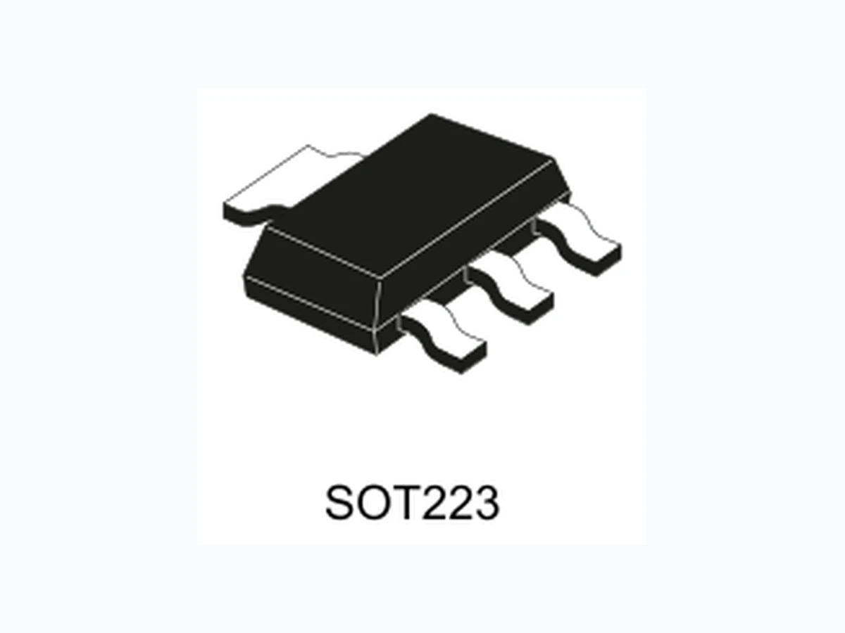
Datasheet - LDL1117 - 1.2 A high PSRR low-dropout linear voltage regulator
Document overview
- Manufacturer or author: STMICROELECTRONICS
- PDF pages: 23
Technical content
Datasheet sections
- 1 Diagram
- 2 Pin configuration
- 3 Typical application
- 4 Maximum ratings
- 5 Electrical characteristics
- 6 Application information
- 6.1 Thermal and short-circuit protections
- 6.2 Input and output capacitor selection
- 7 Typical characteristics
- 8 Package information
- 8.1 SOT223 package information
- 8.2 SOT223 packing information
- 9 Ordering information
Features
- Input voltage from 2.5 V to 18 V
- 20 V AMR
5.0 V (other options are available on request)
- Guaranteed output current 1.2 A
- Typical dropout 350 mV @ 1.2 A
- Internal thermal, current and power limitation
- High PSRR 87 dB @ 120 Hz
- Operating temperature range: -40 °C to 125°C
- Package SOT223
Applications
- Consumer
- Industrial
- SMPS
- Motherboard P.O.L.
- DC-DC post-regulation
Description
The LDL1117 provides 1.2 A of maximum current with an input voltage range from 2.5 V to 18 V, and a typical dropout voltage of 350 mV @ 1.2 A. The high power supply rejection ratio of 87 dB at 120 Hz, rolling down to more than 40 dB at 100 kHz, makes the LDL1117 suitable for direct regulations in SMPS and secondary linear regulations in DC-DC converters. This device includes current limit, SOA and thermal protections. Maturity status link LDL1117
1.2 A high PSRR low-dropout linear voltage regulator
DS12022 - Rev 7 - January 2021 For further information contact your local STMicroelectronics sales office.
1 Diagram
Figure 1. Block diagram
2 Pin configuration
Figure 2. Pin connection (top view) Table 1. Pin description Note: The tab is connected to V OUT.
3 Typical application
Figure 3. Typical application diagram
4 Maximum ratings
Table 2. Absolute maximum ratings operation under these conditions is not implied. Table 3. Thermal data
5 Electrical characteristics
TJ = 25 °C, VIN = VOUT + 1 V or 2.6 V, whichever is greater; CIN = 1 μF; COUT = 4.7 μF; IOUT = 10 mA. Table 4. Electrical characteristics
- V IN = VOUT + 1 V or 2.6 V, whichever is greater.
- Dropout voltage is the input-to-output voltage difference at which the output voltage is 100 mV below its nominal value; this
specification does not apply for nominal output voltages below 2.5 V.
Electrical characteristics
6 Application information
6.1 Thermal and short-circuit protections
The LDL1117 is self-protected from short-circuit conditions and overtemperature. When the output load is higher than the one supported by the device, the output current rises until the limit of typically 2 A is reached. The current limit value is dependent of the dissipated power, thanks to an additional SOA protection, so that the maximum power is limited. The peak current available for a defined drop voltage (VIN-VOUT) is shown in Section 7 . The thermal protection occurs when the junction temperature reaches typically 175 °C. The IC enters the shutdown status. As soon as the junction temperature falls again below 150 °C (typ.) the device starts working again. In order to calculate the maximum power that the device can dissipate, keeping the junction temperature below TJ-OP, the following formula is used: P D M A X = 125 − T A MB / R TH J − A (1) PDMAX should be also derated according to the maximum current allowed by the SOA protection.
6.2 Input and output capacitor selection
The LDL1117 requires external capacitors to assure the regulator control loop stability. Any good quality ceramic capacitor can be used but, the X5R and the X7R are suggested since they guarantee a very stable combination of capacitance and ESR over the temperature range. The input/output capacitors should be placed as close as possible to the relative pins. The LDL1117 requires an input capacitor with a minimum value of 1 μF. The device is also equipped with a differential thermal protection that avoid damage in case of fast thermal gradients inside the chip. When the differential thermal protection is activated both channel and the LDO are switched off. This protection works in auto-retry mode, the device restarts automatically when the thermal conditions go back into the normal operating region. This capacitor must be placed as close as possible to the input pin of the device and returned to a clean analog ground. The control loop of the LDL1117 is designed to work with an output ceramic capacitor. Other type of capacitors may be used, as long as they meet the requirements of minimum capacitance and equivalent series resistance (ESR), as shown in Figure 20 and Figure 21. To assure stability, the output capacitor must maintain its ESR and capacitance in the stable region, over the full operating temperature range. The suggested combination of 1 μF input and 4.7 μF output capacitors offers a good compromise among the stability of the regulator, optimum transient response and total PCB area occupation. LDL1117
Application information
7 Typical characteristics
The following plots are referred to the typical application circuit and, unless otherwise noted, at TA = 25 °C. Figure 4. Output voltage vs. temperature (VIN = 2.6 V, Figure 5. Output voltage vs. temperature (VIN = 2.6 V, Figure 6. Output voltage vs. temperature (VIN = 6 V, Figure 7. Output voltage vs. temperature (VIN = 6 V,
8 Package information
In order to meet environmental requirements, ST offers these devices in different grades of ECOPACK packages, depending on their level of environmental compliance. ECOPACK specifications, grade definitions and product status are available at: www.st.com. ECOPACK is an ST trademark.
8.1 SOT223 package information
Figure 28. SOT223 package outline
Package information
DS12022 - Rev 7 page 14/23
Table 5. SOT223 mechanical data
8.2 SOT223 packing information
Table 6. SOT223 tape and reel mechanical data Figure 29. Tape for SOT223 (dimensions are in mm)
9 Ordering information
Table 7. Order code
Ordering information
DS12022 - Rev 7 page 18/23
Revision history
Table 8. Document revision history 27-Feb-2017 1 Initial release. 04-Jul-2017 3 In Table3: "Thermal data": - thermal data values changed. Minor textchanges. 04-Mar-2020 4 Updated Figure 28. SOT223 package outline. 24-Mar-2020 5 Updated Figure 12. 03-Apr-2020 6 Added Section 8.2 SOT223 packing information.