
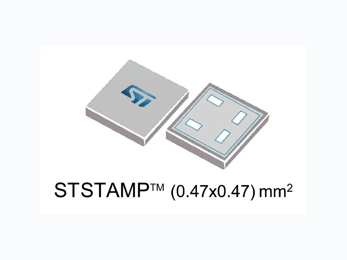
Datasheet - LDBL20 - 200 mA very low quiescent current linear regulator IC in (0.47x0.47) mm² STSTAMP™ package
Document overview
- Manufacturer or author: STMICROELECTRONICS
- PDF pages: 22
Technical content
Datasheet sections
- 1 Diagram
- 2 Pin configuration
- 3 Typical application
- 4 Maximum ratings
- 5 Electrical characteristics
- 6 Application information
- 6.1 Soft-start function
- 6.2 Output discharge function
- 6.3 Input output capacitors
- 7 Typical characteristics
- 8 Recommendation on PCB assembly
- 8.1 PCB design recommendations
- 8.2 Stencil
- 8.3 Solder paste
- 8.4 Placement
- 8.5 Reflow profile
- 9 Package information
- 10 Ordering information
- 10.1 Marking information
Features
- Input voltage from 1.5 to 5.5 V
- Ultra low dropout voltage (200 mV typ. at 200 mA load)
- Very low quiescent current (20 µA typ. at no-load, 0.03 µA typ. in off mode)
- Output voltage tolerance: ± 1.5% @ 25 °C
- 200 mA guaranteed output current
- High PSRR (80 dB@1 kHz, 50 db@100 kHz)
- Wide range of output voltages available on request: from 0.8 V up to 5.0 V in 50 mV step
- Logic-controlled electronic shutdown
- Internal soft-start
- Optional output voltage discharge feature
- Compatible with ceramic capacitor C OUT = 0.47 µF
- Internal constant current and thermal protections
- Available in STSTAMP™ (0.47 x 0.47) mm² package
- Operating temperature range: -40 °C to 125 °C
Applications
- Mobile phones
- Tablet
- Digital still cameras (DSC)
- Wearable devices
- Portable media players
Description
The LDBL20 high accuracy voltage regulator provides 200 mA of maximum current from an input voltage ranging from 1.5 V to 5.5 V, with a typical dropout voltage of 200 mV. It is available in the new STSTAMP™ package, allowing the maximum space saving. The device is stabilized with a ceramic capacitor on the output. The ultra low drop voltage, low quiescent current and low noise features, together with the internal soft- start circuit, make the LDBL20 suitable for low power battery-operated applications. An enable logic control function puts the LDBL20 in shutdown mode with a total current consumption lower than 0.2 µA. Constant current and thermal protection are provided. Maturity status link LDBL20 200 mA very low quiescent current linear regulator IC in (0.47x0.47) mm² STSTAMP™ package LDBL20 Datasheet DS11244 - Rev 3 - January 2021 For further information contact your local STMicroelectronics sales office.
1 Diagram
Figure 1. Block diagram Note: The output discharge MOSFET is optional.
2 Pin configuration
Figure 2. Pin connection Table 1. Pin description
3 OUT Output voltage
4 GND Common ground
1 EN Enable pin logic input: low = shutdown, high = active
2 IN Input voltage
3 Typical application
Figure 3. Typical application circuits
4 Maximum ratings
Table 2. Absolute maximum ratings operation under these conditions is not implied. All values are referred to GND. Table 3. ESD performance Table 4. Thermal performance
5 Electrical characteristics
TJ = 25 °C, VIN = VOUT(NOM) + 1 V or 1.5 V, whichever is greater, CIN = COUT = 1 µF, IOUT = 1 mA, VEN = VIN, unless otherwise specified. Table 5. LDBL20 electrical characteristics
Electrical characteristics
Symbol Parameter Test conditions Min. Typ. Max. Unit COUT Output capacitor Capacitance 0.47 22 µF 1. Not applicable for Vout(nom) > 4.5 V 2. Turn-on time is time measured between the enable input just exceeding VEN high value and the output voltage just reaching 95 % of its nominal value LDBL20
6 Application information
6.1 Soft-start function
The LDBL20 has an internal soft-start circuit. By increasing the startup time up to 100 µs, without the need of any external soft-start capacitor, this feature keeps the regulator inrush current at startup under control.
6.2 Output discharge function
The LDBL20 integrates a MOSFET connected between VOUT and GND. This transistor is activated when the EN pin goes to low logic level and has the function to quickly discharge the output capacitor when the device is disabled by the user. The device is available with or without the auto-discharge feature. See Table 7. Order code.
6.3 Input and output capacitors
The LDBL20 requires external capacitors to assure the regulator control loop stability. Any good quality ceramic capacitor can be used but, the X5R and the X7R are suggested since they guarantee a very stable combination of capacitance and ESR overtemperature. Locating the input/output capacitors as closer as possible to the relative pins is recommended. The LDBL20 requires an input capacitor with a minimum value of 1 μF. This capacitor must be located as closer as possible to the input pin of the device and returned to a clean analog ground. The control loop of the LDBL20 is designed to work with an output ceramic capacitor. This capacitor must meet the requirements of minimum capacitance and equivalent series resistance (ESR), as shown in Figure 17. Stability area vs (COUT, ESR). To assure stability, the output capacitor must maintain its ESR and capacitance in the stable region, over the full operating temperature range. The LDBL20 shows stability with a minimum effective output capacitance of 220 nF. However, to keep stability in all operating conditions (temperature, input voltage and load variations), a minimum output capacitor of 0.47 µF is recommended. The suggested combination of 1 μF input and output capacitors offers a good compromise among the stability of the regulator, optimum transient response and total PCB area occupation. LDBL20
Application information
7 Typical characteristics
Figure 4. Output voltage vs temp. (I OUT = 1 mA) Figure 5. Output voltage vs temp. (I OUT = 200 mA) Figure 6. Line regulation vs temperature Figure 7. Load regulation vs temperature
8 Recommendation on PCB assembly
8.1 PCB design recommendations
- PCB PAD design: non solder mask defined
- PCB pad size: see drawing in Figure 30. STSTAMP™ (0.47x0.47) mm² recommended footprint
- Solder mask opening: 50 μm between the edge of the pad and the edge of the solder mask
- To keep under control the solder paste amount, closed vias are recommended instead of open vias
- The position of tracks and open vias in the solder area should be well balanced. A symmetrical layout is recommended, to reduce the effect of tilt phenomena caused by asymmetrical solder paste amount due to the solder flowing away
8.2 Stencil
- Stencil aperture: see drawing in Figure 31. STSTAMP™ (0.47x0.47) mm² recommended solder stencil
- Stencil thickness: 75 μm
8.3 Solder paste
- 95.8% Sn, 3.5% Ag, 0.7% Cu solder paste
- Halide-free flux qualification ROL0 according to ANSI/J-STD-004
- “No clean” solder paste is recommended.
- Offers a high tack force to resist component movement during high speed
- Solder paste with fine particles: powder particle size is 20-45 μm.• type 4
8.4 Placement
- Manual positioning is not recommended
- It is recommended to use the lead recognition capabilities of the placement system, not the outline centering
- Standard tolerance of ± 0.05 mm is recommended
- 3.5 N placement force is recommended. Too much placement force can lead to squeezed out solder paste and cause solder joints to short. Too low placement force can lead to insufficient contact between package and solder paste that could cause open solder joints or badly centered packages
- To improve the package placement accuracy, a bottom side optical control should be performed with a high resolution tool
- For assembly, a perfect supporting of the PCB (all the more on flexible PCB) is recommended during solder paste printing, pick and place and reflow soldering by using optimized tools LDBL20 Recommendation on PCB assembly DS11244 - Rev 3 page 14/22
8.5 Reflow profile
Figure 28. ST ECOPACK® recommended soldering reflow profile for PCB mounting corresponds to the latest IPC/JEDEC J-STD-020.
9 Package information
In order to meet environmental requirements, ST offers these devices in different grades of ECOPACK packages, depending on their level of environmental compliance. ECOPACK specifications, grade definitions and product status are available at: www.st.com. ECOPACK is an ST trademark. LDBL20
Package information
DS11244 - Rev 3 page 16/22
Figure 29. STSTAMP™ (0.47x0.47) mm² package outline
10 Order code
Table 7. Order code
10.1 Marking information
Figure 32. Marking composition (marking view) Note: The symbol "#" indicates the marking digit, as per Table 7. Order code.
Revision history
Table 8. Document revision history Added Section 8: "Recommendation on PCB assembly". Updated Section 10: "Ordering information". 27-Jan-2021 3 Added new order codes in Table 7.