
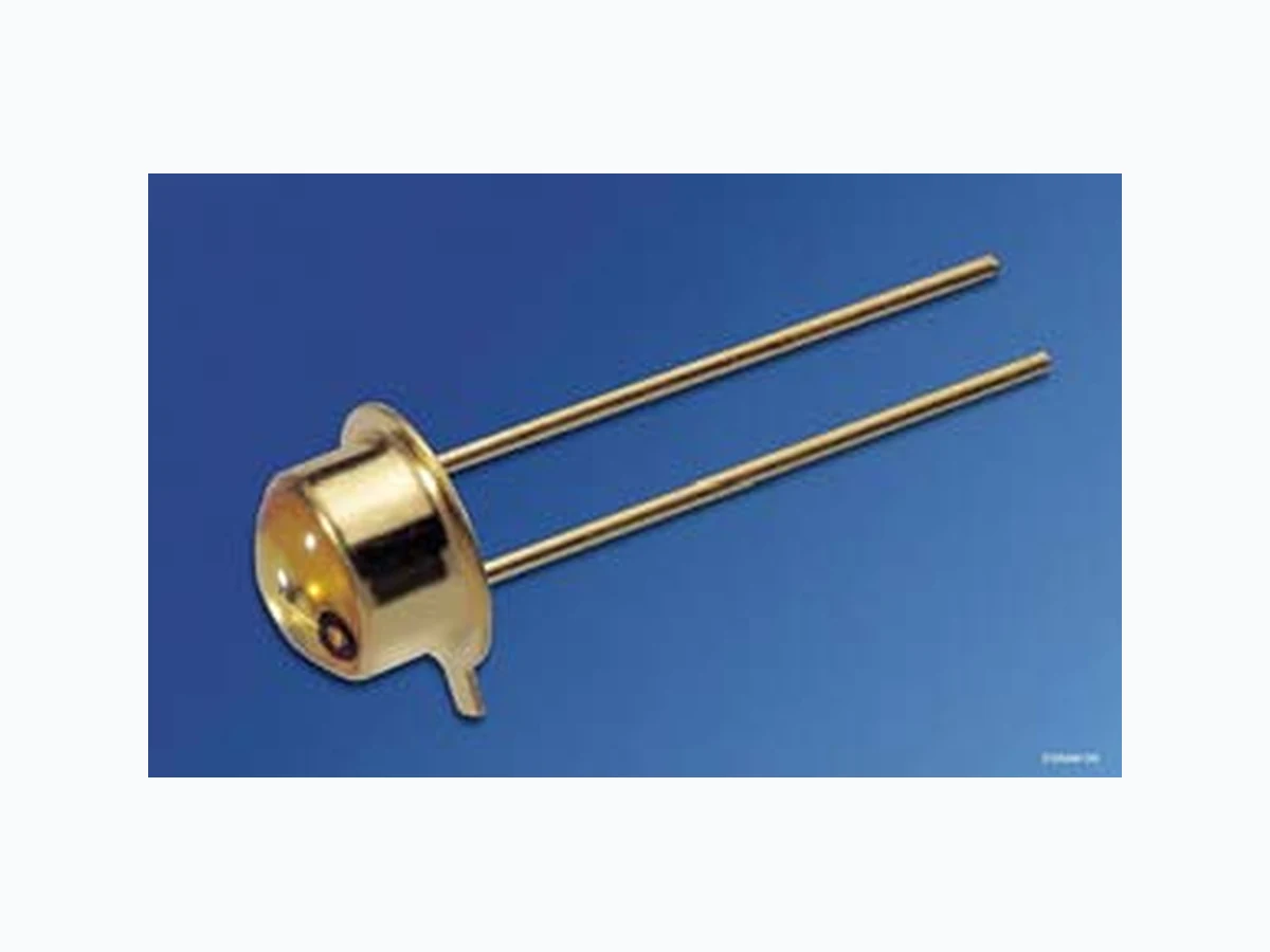
LD242 OSRAM
Document overview
- Manufacturer or author: Provided By www.digicamel.com(FREE DATASHEET DOWNLOAD SITE)
- PDF pages: 7
Technical content
Features
Fabricated in a liquid phase epitaxy process Cathode is electrically connected to the case High reliability Wide beam Same package as BP 103, BPX 63, SFH 464, SFH 483 DIN humidity caregory in acc. with DIN 40 040 GQG
Applications
Photointerrupters Sensor technology Light curtains
Grenzwerte (TA = 25 °C) Maximum Ratings Bezeichnung Parameter Symbol Symbol Wert Value Einheit Unit Betriebs- und Lagertemperatur Operating and storage temperature range Top; Tstg – 40 … + 80 °C Sperrspannung Reverse voltage VR 5 V Durchlassstrom Forward current IF 300 mA Stoßstrom, τ ≤ 10 µs, D = 0 Surge current IFSM 3 A Verlustleistung Power dissipation Ptot 470 mW Wärmewiderstand Thermal resistance RthJA RthJC 450 160 K/W K/W Kennwerte (TA = 25 °C) Characteristics Bezeichnung Parameter Symbol Symbol Wert Value Einheit Unit Wellenlänge der Strahlung Wavelength at peak emission IF = 100 mA, tp = 20 ms λpeak 950 nm Spektrale Bandbreite bei 50% von Imax Spectral bandwidth at 50% of Imax IF = 100 mA, tp = 20 ms ∆λ 55 nm Abstrahlwinkel Half angle ϕ ± 40 Grad deg. Aktive Chipfläche Active chip area A 0.25 mm2 Abmessungen der aktiven Chipfläche Dimension of the active chip area L × B L × W 0.5 × 0.5 mm² Abstand Chipoberfläche bis Linsenscheitel Distance chip surface to lens top H 0.3 … 0.7 mm
Schaltzeiten, Ie von 10% auf 90% und von 90% auf 10%, bei IF = 100 mA, RL = 50 Ω Switching times, Ie from 10% to 90% and from 90% to 10%, IF = 100 mA, RL = 50 Ω tr, tf 1 µs Kapazität Capacitance VR = 0 V Co 40 pF Durchlassspannung Forward voltage IF = 100 mA IF = 1 A, tp = 100 µs VF VF 1.3 (≤ 1.5) 1.9 (≤ 2.5) V V Sperrstrom, VR = 5 V Reverse current IR 0.01 (≤ 1) µA Gesamtstrahlungsfluss Total radiant flux IF = 100 mA, tp = 20 ms Φe 16 mW Temperaturkoeffizient von Ie bzw. Φe, IF = 100 mA Temperature coefficient of Ie or Φe, IF = 100 mA TCI – 0.55 %/K Temperaturkoeffizient von VF, IF = 100 mA Temperature coefficient of VF, IF = 100 mA TCV – 1.5 mV/K Temperaturkoeffizient von λpeak, IF = 100 mA Temperature coefficient of λpeak, IF = 100 mA TCλ 0.3 nm/K Kennwerte (TA = 25 °C) Characteristics (cont’d) Bezeichnung Parameter Symbol Symbol Wert Value Einheit Unit
Gruppierung der Strahlstärke Ie in Achsrichtung gemessen bei einem Raumwinkel Ω = 0.01 sr Grouping of Radiant Intensity Ie in Axial Direction measured at a solid angle of Ω = 0.01 sr Bezeichnung Parameter Symbol Werte Values Einheit Unit LD 242-2 LD 242-3 LD 242 78001) Strahlstärke Radiant intensity IF = 100 mA, tp = 20 ms IF = 1 A, tp = 100 µs Ie Ie typ. 4 … 8 > 6.3 1 … 3.2 mW/sr mW/sr 1) Die Messung der Strahlstärke und des Halbwinkels erfolgt mit einer Lochblende vor dem Bauteil (Durchmesser der Lochblende: 1,1 mm; Abstand Lochblende zu Gehäuserückseite: 4,0 mm). Dadurch wird sichergestellt, dass bei der Strahlstärkemessung nur diejenige Strahl ung in Achsrichtung bewertet wird, die direkt von der Chipoberfläche austritt. Von der Bodenplatte reflektierte Strahlung (vagabundierende Strahlung) wird dagegen nicht bewertet. Diese Reflexionen sind besonders bei Abbildungen der Chipoberfl äche über Zusatzoptiken störend (z.B. Lichtschranken großer Reichweite). In der Anwendung werden im a llgemeinen diese Reflexionen ebenfalls durch Blenden unterdrückt. Durch dieses der Anwendung entsprechende Messverfahren ergibt sich für die Anwender eine besser verwertbare Größe. Diese Lochblendenmessung ist geke nnzeichnet durch den Eintra g „E 7800“, der an die Typenbezeichnung angehängt ist. 1) An aperture is used in front of the component for measurement of the radiant intensity and the half angle (diameter of the aperture: 1.1 mm; distance of aper ture to case back side: 4.0 mm). This ensures that solely the radiation in axial direction emitting directly from the chip surface w ill be evaluated during measurement of the radiant intensity. Radiation reflected by the bottom plate (stray radiation) will not be evaluated. These reflections impair the projection of the chip surface by additional optics (e.g. long-range light reflection switches). In respect of the application of the component, these reflections are generally suppresse d by apertures as well. This measuring procedure corresponding with the application provides more useful values. This aperture measurement is denoted by “E 7800” added to the type designation.
Relative Spectral Emission Irel = f (λ) Forward Current IF = f (VE) Radiation Characteristics Irel = f (ϕ) OHR01938 λ relΙ 880 920 960 1000 nm 1060 100 V OHR01040 F FΙ 110 010 -110 10 -2 A 1.5 2 2.5 33 . 5 4 4.5 typ. max. V OHR01877 02 0 40 60 80 100 1200.40.60.81.0 100 010203040 0.2 0.4 0.6 0.8 1.0ϕ Radiant Intensity Single pulse, tp = 20 µs Permissible Pulse Handling Capability IF = f (τ), TC = 25 °C, duty cycle D = parameter Ie Ie 100 mA = f (IF) Ι OHR01037 F -110 10 0 110 210 10 -2 -1 10 010 A 10 1 Ιe Ιe (100 mA) τ OHR01937 10 -5 s 10 2 Ι F mA 10 -4 10 -3 10 -2 10 0 10 3 10 4 DC 0.5 0.05 0.02 0.01 0.005 D = 0.1 FΙ T Pt Pt T 0.2 Max. Permissible Forward Current IF = f (TA) T OHR00971 A FΙ 02 0 4 0 6 0 8 0 100˚C 100 150 200 250 mA 300 , TC = 160 K/WthJCR RthJA = 450 K/W
Maßzeichnung Package Outlines Maße in mm (inch) / Dimensions in mm (inch). Gehäuse Package
18 A3 DIN 41876 (TO-18), klares Epoxy-Gießharz
18 A3 DIN 41876 (TO-18), transparent epoxy resin
1 = Anode/ anode 2 = Kathode/ cathode ø4.3 (0.169) ø4.1 (0.161) Chip position 3.6 (0.142) 3.0 (0.118) 2.54 (0.100) spacing GETY6625 14.5 (0.571) 12.5 (0.492) ø0.45 (0.018) 2.7 (0.106) 0.9 (0.035) 1.1 (0.043) 0.9 (0.035) 1.1 (0.043) ø5.5 (0.217) ø5.2 (0.205)
Lötbedingungen Soldering Conditions Wellenlöten (TTW) (nach CECC 00802) TTW Soldering (acc. to CECC 00802) Published by OSRAM Opto Semiconductors GmbH Wernerwerkstrasse 2, D-93049 Regensburg www.osram-os.com © All Rights Reserved. The information describes the type of component and shall not be considered as assured characteristics. Terms of delivery and rights to change design reserv ed. Due to technical requirements components may contain dangerous substances. For information on the types in question please contact our Sales Organization. Packing Please use the recycling operators known to you. We can also help you – get in touch with your nearest sales office. By agreement we will take packing material back, if it is sorted. You must bear the costs of tr ansport. For packing material that is returned to us unsorted or which we are not obliged to accept, we shall have to invoice you for any costs incurred. Components used in life-support devices or system s must be expressly authorized for such purpose! Critical components 1 , may only be used in life-support devices or systems 2 with the express written approval of OSRAM OS. 1 A critical component is a component usedin a life-support device or system whose failure can reasonably be expected to cause the failure of that life-support device or system, or to affect its safety or effectiveness of that device or system. 2 Life support devices or systems are intended (a) to be implanted in the human body, or (b) to support and/or maintain and sustain human life. If they fail, it is reasonable to assume that the health of the user may be endangered. OHLY0598 50 100 150 200 250 100 150 200 250 300 T t C s 235 C 10 s C... 260 1. Welle 1. wave 2. Welle 2. wave
5 K/s 2 K/sca 200 K/s
CC... 130100
2 K/s
Zwangskühlung forced cooling Normalkurve standard curve Grenzkurven limit curves