
LCE40P13S LEIDITECH
Document overview
- Manufacturer or author: Provided By www.digicamel.com(FREE DATASHEET DOWNLOAD SITE)
- PDF pages: 6
Technical content
Description
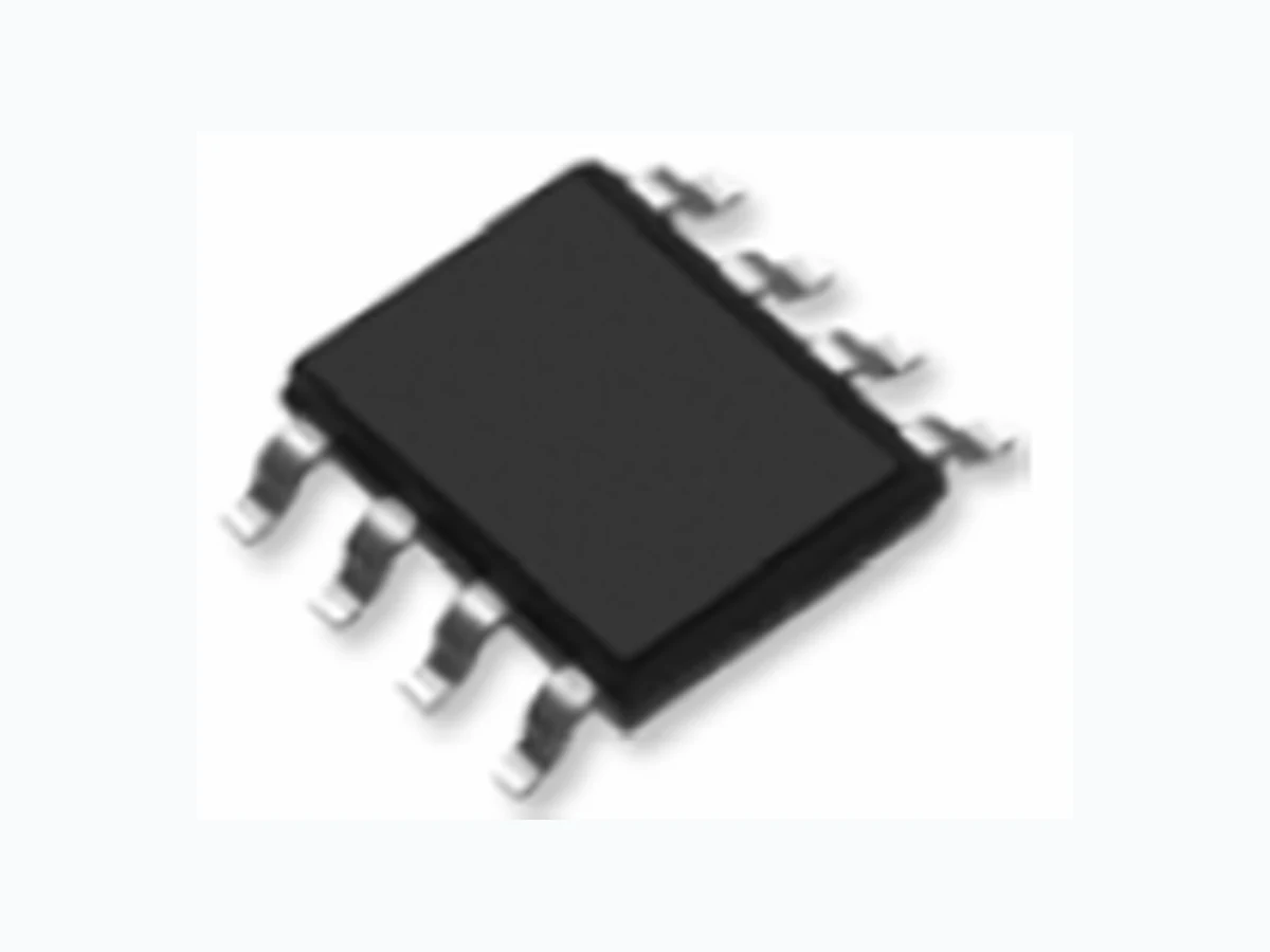
T he LM40P13S uses advanced trench technology and design to provide excellent RDS (ON) w ith low gate charge. It can be used in a wide variety of applications. General Features
- V DS = -40V,ID = -13A RDS (ON) < 15mΩ @ VGS= -10V RDS (ON) < 18mΩ @ VGS= -4.5V
- High density cell design for ultra low Rdson
- Fully characterized avalanche voltage and current
- Excellent package for good heat dissipation Application
- Po wer switching application
- Hard switched and high frequency circuits
- DC-DC converter Schematic dia gram Markin g and pin assignment SOP-8 top view Packag e Marking and Ordering Information De vice Marking Device Device Package Reel Size Tape width Quantity LM4 0P13S SOP-8 Ø330mm 12mm 2500 units Absolute Maximum Ratings (TA=25℃unless otherw ise noted) Parameter S ymbol Limit Unit Drain-S ource Voltage VDS -40 V Gate-Source Voltage VGS ±20 V Drain C urrent-Continuous ID -13 A Drain C urrent-Continuous(TC= Pulse d Drain Current IDM 50 A Maximum Po wer Dissipation PD 2.5 W Operatin g Junction and Storage Temperature Range TJ,TST G -55 T o 150 ℃ Thermal Characteristic T hermal Resistance ,Junction-to-Ambient(Note 2) RθJA 50 /W℃ LM40P13S Enhancement Mode Power MOSFET P-Channel NCE4 0P13S Rev : www.leiditech.com 01.06.2018 1/6
Electrical Characteristics (TA=2 5℃unless otherwise noted) Parameter S ymbol Condition Min Typ Max Unit Off Ch aracteristics Drain-S ource Breakdown Voltage BVDS S V GS=0 V ID= -250μA -40 - - V Z ero Gate Voltage Drain Current IDS S V DS= -40V,VGS=0V - - 1 μA Gate-Bod y Leakage Current IGSS V GS= ±20V,VDS=0V - - ±100 nA On Characteristics (Note 3) Gate T hreshold Voltage VGS( th) V DS=VGS,ID= Drain-S ource On-State Resistance RDS (ON) V GS= -10V, ID= -12A - 12 15 mΩ F orward Transconductance gFS V DS= -15V,ID= -10A 35 - - S D ynamic Characteristics (Note4) Input Cap acitance Clss - 280 0 - PF Output Cap acitance Coss - 320 - PF Revers e Transfer Capacitance Crss VDS= -20V,VGS=0V, F=1.0MHz - 220 - PF S witching Characteristics (Note 4) T urn-on Delay Time td( on) - 11 - nS T urn-on Rise Time tr - 75 - nS T urn-Off Delay Time td( off) - 89 - nS T urn-Off Fall Time tf VDD=-20V, ,RL=2Ω VGS= -10V,RGEN=6Ω - 35 - nS T otal Gate Charge Qg - 40 - nC Gate-Source C harge Qgs - 6 - nC Gate-Drain Charge Qgd VDS= -20V,ID= -12A, VGS= -10V - 12 - nC Drain -Source Diode Characteristics Diod e Forward Voltage (Note 3) VSD V GS=0 V,IS= -12A - - 1.2 V Diod e Forward Current (Note 2) IS - - -13 A Notes: 1. R epetitive Rating: Pulse width limited by maximum junction temperature. 2. Surface Mounted on FR4 Board, t ≤ 10 sec. 3. Pulse Test: Pulse Width ≤ 300μs, Duty Cycle ≤ 2%. 4. Guaranteed by design, not subject to production LM40P13S Rev : www.leiditech.com 01.06.2018 2/6
1) EAS Test Circuit 2) Gate Cha rge Test Circuit 3) S witch Time Test Circuit LM40P13S Rev : www.leiditech.com 01.06.2018 3/6
limeters Dimensions In Inches Sy mbol Min. Max. Min. Max. A 1.350 1.750 0.053 0.069 A1 0.100 0.250 0.004 0.010 A2 1.350 1.550 0.053 0.061 b 0.330 0.510 0.013 0.020 c 0.170 0.250 0.006 0.010 D 4.700 5.100 0.185 0.200 E 3.800 4.000 0.150 0.157 E1 5.800 6.200 0.228 0.244 e 1.270(BS C) 0.050(BSC) L 0.400 1.270 0.016 0.050 θ 0° 8 ° 0 ° 8 ° LM40P13S Sha nghai Leiditech Electronic Co.,Ltd Email: sale1@leiditech.com Tel : +86- 021 50828806 Fax : +86- 021 50477059 Rev : www.leiditech.com 01.06.2018 6/6