
LCC VISHAY
Document overview
- Manufacturer or author: Provided By www.digicamel.com(FREE DATASHEET DOWNLOAD SITE)
- PDF pages: 4
Technical content
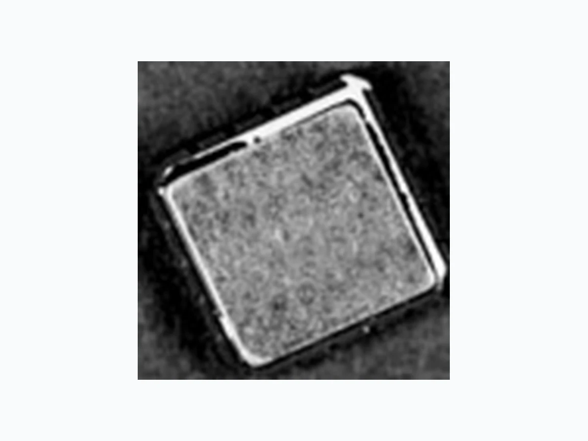
LCC, TLCC Vishay Thin Film Document Number: 60012 For technical questions, contact: thin-film@vishay.com www.vishay.com Revision: 31-Jul-08 37 Hermetic, 50 Mil Pitch, Leadless Chip Resistor Networks SURFACE MOUNT NETWORKS Vishay Thin Film offers a wide resistance range in 16, 20, and 24 terminal hermetic leadless chip carriers. The standard circuits in the ohmic ranges listed below will utilize the outstanding wraparound terminations developed for chip resistors. Should one of the standards not fit your application, consult the factory for a custom circuit.
FEATURES
- Lead (Pb)-free available
- High purity alumina substrate for high power dissipation
- Leach resistant terminations with nickel barrier
- 16, 20, 24 terminal gold plated wraparound true hermetic packaging
- Military/Aerospace
- Hermetically sealed
- Isolated/Bussed circuits
- Ideal for military/aerospace applications TYPICAL PERFORMANCE Resistance range: Noted on schematics SCHEMATIC * Pb containing terminations are not RoHS compliant, exemptions may apply Actual Size ABS TRACKING TCR 25 5 ABS RATIO TOL 0.1 NA Available Pb-free RoHS* COMPLIANT (10 Isolated Resistors) (19 Resistors + 1 Common Point) 13 12 11 10 9 19 20 1 2 3 13 12 11 10 9 19 20 1 2 3 10 9 8 7 15 16 1 2 13 12 11 10 22 23 1 2 3 14 15 13 12 11 10 9 19 20 1 2 3 13 12 11 10 22 24 1 2 3 14 15 10 9 8 7 15 1 2 13 12 11 10 9 19 20 1 2 3 10 9 8 7 15 1 2 16 14 3 13 12 11 10 22 24 1 2 3 14 15 13 12 11 10 9 19 20 1 2 3 TLCC 16 A01 1 kΩ - 100 kΩ TLCC 20 A01 10 - 200 kΩ TLCC 24 A01 1 kΩ - 100 kΩ TLCC 16 A03 100 Ω - 100 kΩ TLCC 20 A03 10 Ω - 120 kΩ TLCC 24 A03 1 kΩ - 100 kΩ TLCC 16 A06 100 Ω - 100 kΩ TLCC 20 A06 1 kΩ - 110 kΩ TLCC 24 A06 1 kΩ - 100 kΩ 10 Ω - 250 kΩ 10 Ω - 200 kΩ LCC 20A LCC 20B
LCC, TLCC Vishay Thin Film Hermetic, 50 Mil Pitch, Leadless Chip Resistor Networks www.vishay.com For technical questi ons, contact: thin-film@vishay.com Document Number: 60012 SURFACE MOUNT NETWORKS Note
- Tantalum nitride film is custom, consult factory DIMENSIONS in inches and millimeters STANDARD ELECTRICAL SPECIFICATIONS TEST SPECIFICATIONS CONDITIONS Material Passivated nichrome TCR: Tracking ± 5 ppm/°C - 55 °C to + 125 °C Absolute ± 25 ppm/°C, ± 50 ppm/°C, ± 100 ppm/°C and ± 300 ppm/°C - 55 °C to + 125 °C Tolerance: Ratio N/a Power Rating: Resistor 50 mW max. (common circuits); 100 mW ma x. (isolated circuits) Max. at + 70 °C Package 500 mW Max. at + 70 °C Stability: ΔR Absolute 0.1 % 2000 h at + 70 °C ΔR Ratio 0.03 % 2000 h at + 70 °C Voltage Coefficient < 5 ppm/V typical Working Voltage 100 V Operating Temperature Range - 55 °C to + 125 °C Storage Temperature Range - 55 °C to + 150 °C Noise < - 30 dB Thermal EMF 0.008 µV/°C Shelf Life Stability: Absolute 100 ppm 1 year at + 25 °C Ratio 20 ppm 1 year at + 25 °C ABCDEFGH B D max. G typ. A typ. E typ. H Index corner F C Terminal #1 indicator Terminal #1 0.008" (0.203) R typ.
LCC, TLCC Hermetic, 50 Mil Pitch, Leadless Chip Resistor Networks Vishay Thin Film Document Number: 60012 For technical questions, contact: thin-film@vishay.com www.vishay.com Revision: 31-Jul-08 39 SURFACE MOUNT NETWORKS Note (1) LCC or LCCT only available in 20 pin size MECHANICAL SPECIFICATIONS Resistive Element Passivated nichrome Substrate Material Alumina Body Ceramic Terminals Gold over nickel Marking Resistance to Solvents Per MIL-PRF-83401 Lead (Pb)-free Option 96.5 % Sn, 3.0 % Ag, 0.5 % Cu Lead (Pb)-free Finish Hot solder dip GLOBAL PART NUMBER INFORMATION New Global Part Numbering: TLCC20AE1002BUF (preferred part number format) GLOBAL MODEL (4 or 5 digits) TERMINAL COUNT (1) SCHEMATICS (4 or 5 digits) TCR CHARACTERISTICS RESISTANCE TOLERANCE PACKAGING LCC (Tin lead) LCCT (Tin lead) TLCC (Lead (Pb)-free) TLCCT (Lead (Pb)-free) (e1) A =I s o l a t e d resistors B = Resistor to common bus A01 = Resistor to common bus A03 = Isolated parallel resistor A06 =I s o l a t e d adjacent resistor E = 25 ppm/°C H = 50 ppm/°C K = 100 ppm/°C M = 300 ppm/°C First 3 digits are significant figures and the last digit specifies the number of zeroes to follow. Example: 10R0 = 10 Ω 12R5 = 12.5 Ω 1000 = 100 Ω 1001 = 1000 Ω B = 0.1 % D = 0.5 % F = 1 % G = 2 % J = 5 % K = 10 % S = Special TAPE AND REEL T0 = 100 min. 100 mult T1 = 1000 min. 1000 mult T3 = 300 min. 300 mult T5 = 500 min. 500 mult TF = Full reel 2000 TS = 100 min. 1 mult UF = TUBED Historical Part Number example: LC20BK1003J (will continue to be accepted) LC 20 B K 1003 J SERIES PINS SCHEMATIC TCR CHARACTERISTIC RESISTANCE TOLERANCE CT16A01K 1003 K TLC UF C20 A E 1002 B TLC UF
Document Number: 91000 www.vishay.com Revision: 18-Jul-08 1 Disclaimer Legal Disclaimer Notice Vishay All product specifications and data are subject to change without notice. Vishay Intertechnology, Inc., its affiliates, agents, and employees, and all persons acting on its or their behalf (collectively, “Vishay”), disclaim any and all liability for any errors, inaccuracies or incompleteness contained herein or in any other disclosure relating to any product. Vishay disclaims any and all li ability arising out of the use or application of any product described herein or of any information provided herein to the maximum extent permit ted by law. The product specifications do not expand or otherwise modify Vishay’s terms and conditions of purcha se, including but not limited to the warranty expressed therein, which apply to these products. No license, express or implied, by estoppel or otherwise, to any intellectual property rights is granted by this document or by any conduct of Vishay. The products shown herein are not designed for use in medi cal, life-saving, or life-sustaining applications unless otherwise expressly indicated. Customers using or selling Vishay products not expressly indicated for use in such applications do so entirely at their own risk and agree to fully indemnify Vishay for any damages arising or resulting from such use or sale. Please contact authorized Vishay personnel to obtain written terms and conditions regarding products designed for such applications. Product names and markings noted herein may be trademarks of their respective owners.