


 Download PDF
LC8220 SANYO
Document overview
- PDF pages: 13
Technical content
Page 1
Ordering number : EN\*4909A
CMOS LSI

Preliminaly
Overview
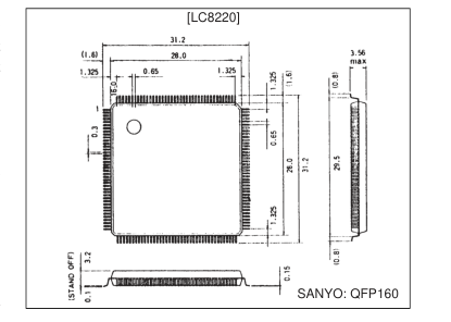
Package Dimensions
The LC8220 JPEG LSI implements digital still image
unit: mm
compression and decompression conforming to the JPEG
3153A-QFP160
(Joint Photographic Expert Group) standard. The LC8220
includes the baseline system of the ISO 10918 (JPEG) standard, and requires no external components to construct an application that performs JPEG compliant compression/decompression.
Features
- Conforms to the ISO 10918-1 baseline system
- Four quantization tables and four Huffman tables (two for AC and two for DC) are built in.
- Hardware support for JPEG marker codes
- Built-in bidirectional YUV - RGB converter
- Many color component sampling ratios are supported. (e.g., YUV 4:1:1 and YMCK 1:1:1:1, etc.)
- Level shift function that can be defined for each component
- Built-in dual buffers for reduced data transfer load
- Bus sizing function that allows direct connection to 8-, 16-, and 32-bit busses
- Endian control function
- Three independent data buses
SANYO Electric Co.,Ltd. Semiconductor Bussiness Headquarters
TOKYO OFFICE Tokyo Bldg., 1-10, 1 Chome, Ueno, Taito-ku, TOKYO, 110 JAPAN
32896HA (OT)/D1694TH (OT) No. 4909-1/13
Page 2
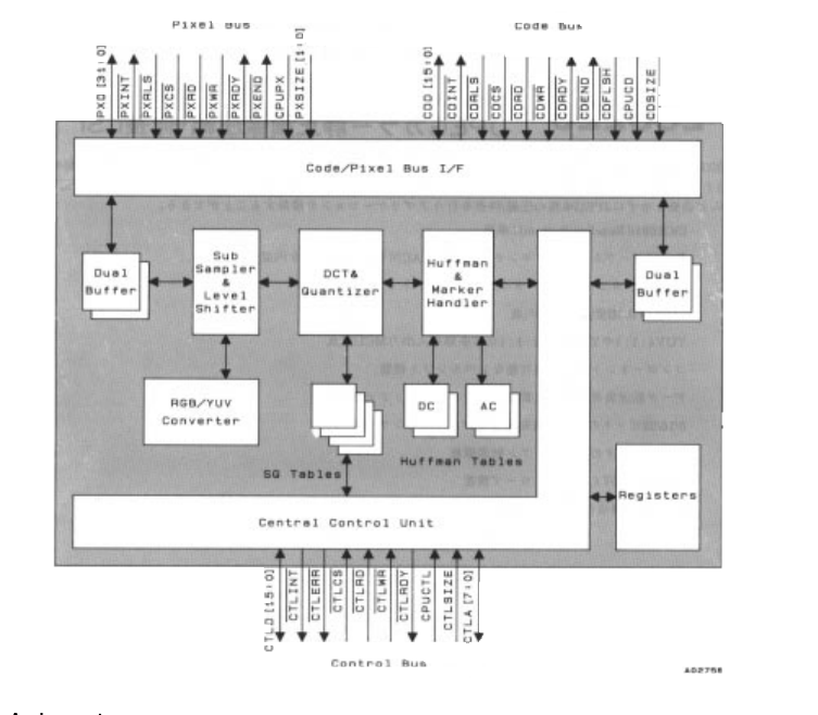
Block Diagram
The LC8220 has three independent buses.
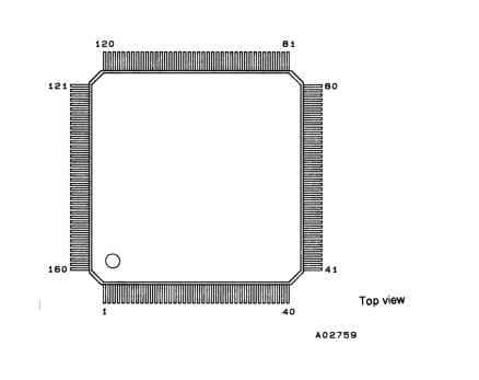
Pin Assignment
No. 4909-2/13
Page 3
Pin Functions
| Pin No. | Symbol | I/O | Function |
|---|---|---|---|
| 1 | VSS | — | Ground |
| 2 | CTLCS | I | Control bus chip select*2 |
| 3 | CTLRD | I | Control bus read request*3 |
| 4 | CTLWR | I | Control bus write request*4 |
| 5 | CTLRDY | O | Control bus ready for read/write requests*5 |
| 6 | CTLERR | O | Error interrupt request |
| 7 | CTLINT | O | Control bus interrupt request |
| 8 | CPUCTL | I | Connected CPU type setting for the control bus*1 |
| 9 | CTLSIZE | I | Bus width selection for the control bus (0: 8 bits, 1: 16 bits) |
| 10 | VDD | — | +5 V power supply |
| 11 | VSS | — | Ground |
| 12 | CTLA7 | I | Control address bus |
| 13 | CTLA6 | I | |
| 14 | CTLA5 | I | |
| 15 | CTLA4 | I | |
| 16 | CTLA3 | I | |
| 17 | CTLA2 | I | |
| 18 | CTLA1 | I | |
| 19 | CTLA0 | I | |
| 20 | VDD | — | +5 V power supply |
| 21 | VSS | — | Ground |
| 22 | CTLD15 | I/O | Control data bus (D15 to D8 are unused if an 8-bit CPU is used.*7) |
| 23 | CTLD14 | I/O | |
| 24 | CTLD13 | I/O | |
| 25 | CTLD12 | I/O | |
| 26 | CTLD11 | I/O | |
| 27 | CTLD10 | I/O | |
| 28 | CTLD9 | I/O | |
| 29 | CTLD8 | I/O | |
| 30 | VDD | — | +5 V power supply |
| 31 | VSS | — | Ground |
| 32 | CTLD7 | I/O | Control data bus |
| 33 | CTLD6 | I/O | |
| 34 | CTLD5 | I/O | |
| 35 | CTLD4 | I/O | |
| 36 | CTLD3 | I/O | |
| 37 | CTLD2 | I/O | |
| 38 | CTLD1 | I/O | |
| 39 | CTLD0 | I/O | |
| 40 | VDD | — | +5 V power supply |
| 41 | VSS | — | Ground |
| 42 | CLK | I | System clock |
| 43 | CLKSEL | I | Clock divisor selection (0: no divisor, 1: divisor used)*6 |
| 44 | RESET | I | System reset |
| 45 | TEST | I | Test mode selection (0: normal operation, 1: test mode)*6 |
| 46 | TESTOUT | O | Test result output*8 |
| 47 | MDD10 | I/O | Test mode data bus*7 |
| 48 | MDD9 | I/O | |
| 49 | MDD8 | I/O | |
| 50 | VDD | — | +5 V power supply |
| 51 | VSS | — | Ground |
| 52 | MDD7 | I/O | Test mode data bus*7 |
| 53 | MDD6 | I/O | |
| 54 | MDD5 | I/O |
Continued on next page.
No. 4909-3/13
Page 4
Continued from preceding page.
| Pin No. | Symbol | I/O | Function |
|---|---|---|---|
| 55 | MDD4 | I/O | Test mode data bus*7 |
| 56 | MDD3 | I/O | |
| 57 | MDD2 | I/O | |
| 58 | MDD1 | I/O | |
| 59 | MDD0 | I/O | |
| 60 | VDD | — | +5 V power supply |
| 61 | VSS | — | Ground |
| 62 | TESTI1 | I | Test mode input pins*9 |
| 63 | TESTI2 | I | |
| 64 | TESTI3 | I | |
| 65 | TESTI4 | I | |
| 66 | TESTI5 | I | |
| 67 | TESTO1 | O | Test mode output pins*8 |
| 68 | TESTO2 | O | |
| 69 | TESTI6 | I | Test mode input pin*9 |
| 70 | TESTO3 | O | Test mode output pin*8 |
| 71 | CPUPX | I | Connected CPU type setting for the pixel bus*1 |
| 72 | PXCS | I | Pixel bus chip select*2 |
| 73 | PXRD | I | Pixel bus read request*3 |
| 74 | PXWR | I | Pixel bus write request*4 |
| 75 | PXRDY | O | Pixel bus ready for read/write requests*5 |
| 76 | PXINT | O | Pixel bus interrupt request |
| 77 | PXRLS | I | Pixel bus interrupt release |
| 78 | PXEND | O | Pixel bus last data output indicator |
| 79 | (NC) | — | |
| 80 | VDD | — | +5 V power supply |
| 81 | VSS | — | Ground |
| 82 | PXD31 | I/O | Pixel data bus (D31 to D16 are unused if a 16-bit CPU is used and D31 to D8 are unused if an 8-bit CPU is used.*7) |
| 83 | PXD30 | I/O | |
| 84 | PXD29 | I/O | |
| 85 | PXD28 | I/O | |
| 86 | PXD27 | I/O | |
| 87 | PXD26 | I/O | |
| 88 | PXD25 | I/O | |
| 89 | PXD24 | I/O | |
| 90 | VDD | — | +5 V power supply |
| 91 | VSS | — | Ground |
| 92 | PXD23 | I/O | Pixel data bus (D31 to D16 are unused if a 16-bit CPU is used and D31 to D8 are unused if an 8-bit CPU is used.*7) |
| 93 | PXD22 | I/O | |
| 94 | PXD21 | I/O | |
| 95 | PXD20 | I/O | |
| 96 | PXD19 | I/O | |
| 97 | PXD18 | I/O | |
| 98 | PXD17 | I/O | |
| 99 | PXD16 | I/O | |
| 100 | VDD | — | +5 V power supply |
| 101 | VSS | — | Ground |
| 102 | PXD15 | I/O | Pixel data bus (D31 to D16 are unused if a 16-bit CPU is used and D31 to D8 are unused if an 8-bit CPU is used.*7) |
| 103 | PXD14 | I/O | |
| 104 | PXD13 | I/O | |
| 105 | PXD12 | I/O | |
| 106 | PXD11 | I/O | |
| 107 | PXD10 | I/O | |
| 108 | PXD9 | I/O | |
| 109 | PXD8 | I/O |
Continued on next page.
No. 4909-4/13
Page 5
Continued from preceding page.
| Pin No. | Symbol | I/O | Function |
|---|---|---|---|
| 110 | VDD | — | +5 V power supply |
| 111 | VSS | — | Ground |
| 112 | PXD7 | I/O | Pixel data bus |
| 113 | PXD6 | I/O | |
| 114 | PXD5 | I/O | |
| 115 | PXD4 | I/O | |
| 116 | PXD3 | I/O | |
| 117 | PXD2 | I/O | |
| 118 | PXD1 | I/O | |
| 119 | PXD0 | I/O | |
| 120 | VDD | — | +5 V power supply |
| 121 | VSS | — | Ground |
| 122 | PXSIZE0 | I | Bus width selection for the pixel bus (PXSIZE [1,0] = 00: 8 bits, 01: 16 bits, 1*: 32 bits) |
| 123 | PXSIZE1 | I | |
| 124 | (NC) | — | |
| 125 | CDCS | I | Code bus chip select*2 |
| 126 | CDRD | I | Code bus read request*3 |
| 127 | CDWR | I | Code bus write request*4 |
| 128 | CDRDY | O | Code bus ready for read/write requests*5 |
| 129 | CDINT | O | Code bus interrupt request |
| 130 | CDRLS | I | Code bus interrupt release |
| 131 | CDEND | O | Code bus last data output |
| 132 | CDFLSH | I | Code bus forcible buffer flush |
| 133 | (NC) | — | |
| 134 | (NC) | — | |
| 135 | (NC) | — | |
| 136 | (NC) | — | |
| 137 | (NC) | — | |
| 138 | CPUCD | I | Connected CPU type setting for the code bus*1 |
| 139 | CDSIZE | I | Bus width setting for the code bus (0: 8 bits, 1: 16 bits) |
| 140 | VDD | — | +5 V power supply |
| 141 | VSS | — | Ground |
| 142 | CDD15 | I/O | Code data bus (D15 to D8 are unused if an 8-bit CPU is used.*7) |
| 143 | CDD14 | I/O | |
| 144 | CDD13 | I/O | |
| 145 | CDD12 | I/O | |
| 146 | CDD11 | I/O | |
| 147 | CDD10 | I/O | |
| 148 | CDD9 | I/O | |
| 149 | CDD8 | I/O | |
| 150 | VDD | — | +5 V power supply |
| 151 | VSS | — | Ground |
| 152 | CDD7 | I/O | Code data bus |
| 153 | CDD6 | I/O | |
| 154 | CDD5 | I/O | |
| 155 | CDD4 | I/O | |
| 156 | CDD3 | I/O | |
| 157 | CDD2 | I/O | |
| 158 | CDD1 | I/O | |
| 159 | CDD0 | I/O | |
| 160 | VDD | — | +5 V power supply |
Note 1, 2, 3, 4, 5: These items are related to the CPU type.
| Z**CS2 | Z**RD3 | Z**WR4 | Z**RDY5 | |
| 8086 family CPU (CPU = 1) | CS | RD | WR | RDY |
| 68000 family CPU (CPU = 0) | AS | R/W | DS | ACK |
Connect to VSS (ground). 6: 7: Must be pulled up. 8: These are NC pins. Connect to VDD. 9:
No. 4909-5/13
Page 6
Specifications
Absolute Maximum Ratings at Ta = 25°C, GND = 0 V
| Parameter | Symbol | Conditions | Ratings | Unit |
|---|---|---|---|---|
| Maximum supply voltage | VDD max | –0.3 to +7.0 | V | |
| I/O voltages | VI, VO | –0.3 to VDD + 0.3 | V | |
| Operating temperature | Topr | –30 to +70 | °C | |
| Storage temperature | Tstg | –55 to +125 | °C | |
| Soldering temperature | Hand soldering: 3 seconds | 350 | °C | |
| Reflow soldering: 10 seconds | 235 | °C |
Allowable Operating Ranges at Ta = –30 to +70°C, GND = 0 V
| Parameter | Symbol | Conditions | min | typ | max | Unit |
|---|---|---|---|---|---|---|
| Supply voltage | VDD | 4.5 | 5.5 | V | ||
| Input voltage | VIN | 0 | VDD | V |
DC Characteristics at Ta = –30 to +70°C, VDD = 4.5 to 5.5 V, GND = 0 V
| Parameter | Symbol | Conditions | min | typ | max | Unit |
|---|---|---|---|---|---|---|
| Input high level voltage | VIH | TTL compatible: CTLCS, CTLRD, CTLWR, CPUCTL, CTLSIZE, CTLA7 to CTLA0, CLKSEL, RESET, TEST, CTLD15 to CTLD0 | 2.2 | V | ||
| Input low level voltage | VIL | TTL compatible: CPUPX, PXCS, PXRD, PXWR, PXD31 to PXD0, PXRLS, PXSIZE0 | 0.8 | V | ||
| Input leakage current | IL | PXSIZE1, CDCS, CDRD, CDWR, CDRLS, CDFLSH, CPUCD, CDSIZE, CDD15 to CDD0 | –10 | +10 | µA | |
| Output high level voltage | VOH | IOH = –3 mA, TTL compatible: CTLRDY, CTLERR, CTLINT, TESTOUT, CTLD15 to CTLD0, PXRDY, PXINT, PXEND, PXD31 to PXD0, CDRDY, CDINT, CDEND, CDD15 to CDD0 | VDD – 2.1 | V | ||
| Output low level voltage | VOL | IOH = –3 mA, TTL compatible: CTLRDY, CTLERR, CTLINT, TESTOUT, CTLD15 to CTLD0, PXRDY, PXINT, PXEND, PXD31 to PXD0, CDRDY, CDINT, CDEND, CDD15 to CDD0 | 0.4 | V | ||
| Output leakage current | IOZ | For high impedance outputs: CTLD15 to CTLD0, PXD31 to PXD0, CDD15 to CDD0 | –10 | +10 | µA | |
| Oscillator frequency | fOSC | CLK | 16.67 | MHz | ||
| Current drain | IDD | VDD = 5.0 V | 145 | mA |
No. 4909-6/13
Page 7
AC Characteristics
Code Bus Interface Timing
Code Bus Read Cycle
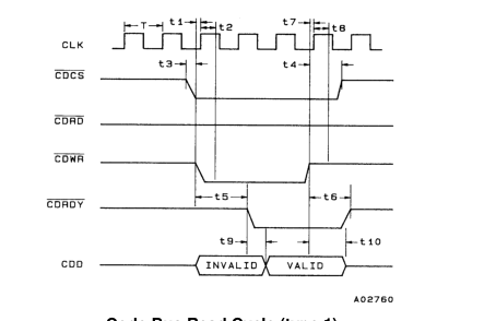
Code Bus Read Cycle (type 1)
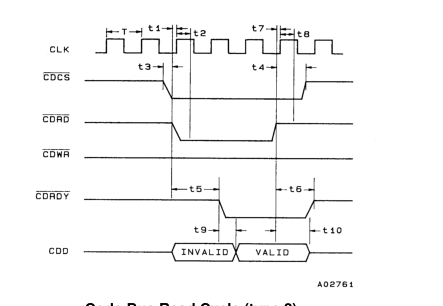
Code Bus Read Cycle (type 2)
| Item | Minimum | Maximum | Unit | |
|---|---|---|---|---|
| t1 | Read signal assert setup time (referenced to CLK) | 8 | ns | |
| t2 | Read signal assert hold time (referenced to CLK) | 15 | ns | |
| t3 | Chip select stabilization time (referenced to the read signal) | 0 | ns | |
| t4 | Chip select hold time (referenced to the read signal) | 0 | ns | |
| t5 | Ready signal response delay time (referenced to the read signal) | T + t1 + 20 | ns | |
| t6 | Ready signal release delay time (referenced to the read signal) | t7 + 27 | ns | |
| t7 | Read signal negate setup time (referenced to CLK) | 8 | ns | |
| t8 | Read signal negate hold time (referenced to CLK) | 15 | ns | |
| t9 | Data output delay time (referenced to the ready signal) | 15 | ns | |
| t10 | Data output hold time (referenced to the read signal) | t7 + 15 | ns | |
| T | Clock period | 60 | ns |
No. 4909-7/13
Page 8
Code Bus Write Cycle
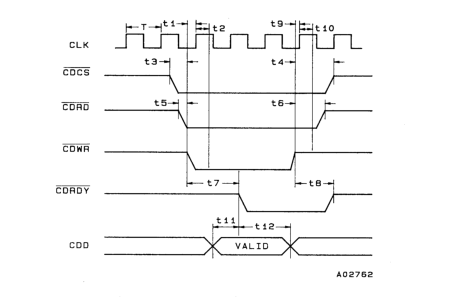
Code Bus Write Cycle (type 1)
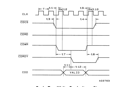
Code Bus Write Cycle (type 2)
| Item | Minimum | Maximum | Unit | |
|---|---|---|---|---|
| t1 | Write signal assert setup time (referenced to CLK) | 8 | ns | |
| t2 | Write signal assert hold time (referenced to CLK) | 15 | ns | |
| t3 | Chip select stabilization time (referenced to the write signal) | 0 | ns | |
| t4 | Chip select hold time (referenced to the write signal) | 0 | ns | |
| t5 | Write cycle selection signal stabilization time (referenced to the write signal) | 0 | ns | |
| t6 | Write cycle selection signal hold time (referenced to the write signal) | 0 | ns | |
| t7 | Ready signal response delay time (referenced to the write signal) | T + t1 + 20 | ns | |
| t8 | Ready signal release delay time (referenced to the write signal) | t9 + 27 | ns | |
| t9 | Write signal negate setup time (referenced to CLK) | 8 | ns | |
| t10 | Write signal negate hold time (referenced to CLK) | 15 | ns | |
| t11 | Data setup time (referenced to the ready signal) | 45 | ns | |
| t12 | Data hold time (referenced to the ready signal) | 15 | ns | |
| T | Clock period | 60 | ns |
No. 4909-8/13
Page 9
Pixel Bus Interface Timing
Pixel Bus Read Cycle
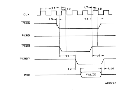
Pixel Bus Read Cycle (type 1)
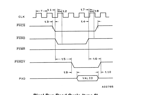
Pixel Bus Read Cycle (type 2)
| Item | Minimum | Maximum | Unit | |
|---|---|---|---|---|
| t1 | Read signal assert setup time (referenced to CLK) | 8 | ns | |
| t2 | Read signal assert hold time (referenced to CLK) | 15 | ns | |
| t3 | Chip select stabilization time (referenced to the read signal) | 5 | ns | |
| t4 | Chip select hold time (referenced to the read signal) | 5 | ns | |
| t5 | Ready signal response delay time (referenced to the read signal) | T + t1 + 20 | ns | |
| t6 | Ready signal release delay time (referenced to the read signal) | t7 + 28 | ns | |
| t7 | Read signal negate setup time (referenced to CLK) | 8 | ns | |
| t8 | Read signal negate hold time (referenced to CLK) | 15 | ns | |
| t9 | Data output delay time (referenced to the ready signal) | 15 | ns | |
| t10 | Data output hold time (referenced to the read signal) | t7 + 18 | ns | |
| T | Clock period | 60 | ns |
No. 4909-9/13
Page 10
Pixel Bus Write Cycle
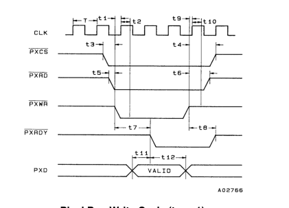
Pixel Bus Write Cycle (type 1)
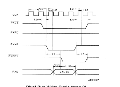
Pixel Bus Write Cycle (type 2)
| Item | Minimum | Maximum | Unit | |
|---|---|---|---|---|
| t1 | Write signal assert setup time (referenced to CLK) | 8 | ns | |
| t2 | Write signal assert hold time (referenced to CLK) | 15 | ns | |
| t3 | Chip select stabilization time (referenced to the write signal) | 5 | ns | |
| t4 | Chip select hold time (referenced to the write signal) | 5 | ns | |
| t5 | Write cycle selection signal stabilization time (referenced to the write signal) | 5 | ns | |
| t6 | Write cycle selection signal hold time (referenced to the write signal) | 5 | ns | |
| t7 | Ready signal response delay time (referenced to the write signal) | T + t1 + 20 | ns | |
| t8 | Ready signal release delay time (referenced to the write signal) | t9 + 28 | ns | |
| t9 | Write signal negate setup time (referenced to CLK) | 8 | ns | |
| t10 | Write signal negate hold time (referenced to CLK) | 15 | ns | |
| t11 | Data setup time (referenced to the ready signal) | 60 | ns | |
| t12 | Data hold time (referenced to the ready signal) | 20 | ns | |
| T | Clock period | 60 | ns |
No. 4909-10/13
Page 11
Control Bus Interface Timing
Control Bus Read Cycle
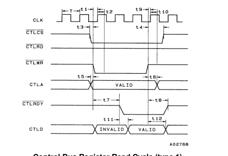
Control Bus Register Read Cycle (type 1)
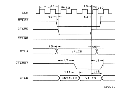
Control Bus Register Read Cycle (type 2)
| Item | Minimum | Maximum | Unit | |
|---|---|---|---|---|
| t1 | Read signal assert setup time (referenced to CLK) | 10 | ns | |
| t2 | Read signal assert hold time (referenced to CLK) | 15 | ns | |
| t3 | Chip select stabilization time (referenced to the read signal) | 10 | ns | |
| t4 | Chip select hold time (referenced to the read signal) | 15 | ns | |
| t5 | Address stabilization time (referenced to the read signal) | 0 | ns | |
| t6 | Address hold time (referenced to the read signal) | 5 | ns | |
| t7 | Ready signal response delay time (referenced to the read signal) | T + t1 + 24 | ns | |
| t8 | Ready signal release delay time (referenced to the read signal) | t9 + 30 | ns | |
| t9 | Read signal negate setup time (referenced to CLK) | 12 | ns | |
| t10 | Read signal negate hold time (referenced to CLK) | 15 | ns | |
| t11 | Data output delay time (referenced to the ready signal) | 0 | ns | |
| t12 | Data output hold time (referenced to the read signal) | t9 + 30 | ns | |
| T | Clock period | 60 | ns |
No. 4909-11/13
Page 12
Control Bus Write Cycle
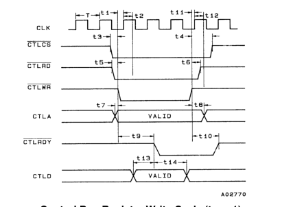
Control Bus Register Write Cycle (type 1)
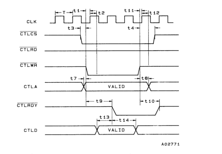
Control Bus Register Write Cycle (type 2)
| Item | Minimum | Maximum | Unit | |
|---|---|---|---|---|
| t1 | Write signal assert setup time (referenced to CLK) | 12 | ns | |
| t2 | Write signal assert hold time (referenced to CLK) | 15 | ns | |
| t3 | Chip select stabilization time (referenced to the write signal) | 10 | ns | |
| t4 | Chip select hold time (referenced to the write signal) | 15 | ns | |
| t5 | Write cycle selection signal stabilization time (referenced to the write signal) | 10 | ns | |
| t6 | Write cycle selection signal hold time (referenced to the write signal) | 10 | ns | |
| t7 | Address stabilization time (referenced to the write signal) | 0 | ns | |
| t8 | Address hold time (referenced to the write signal) | 5 | ns | |
| t9 | Ready signal response delay time (referenced to the write signal) | T + t1 + 24 | ns | |
| t10 | Ready signal release delay time (referenced to the write signal) | t11 + 32 | ns | |
| t11 | Write signal negate setup time (referenced to CLK) | 5 | ns | |
| t12 | Write signal negate hold time (referenced to CLK) | 15 | ns | |
| t13 | Data setup time (referenced to the ready signal) | 60 | ns | |
| t14 | Data hold time (referenced to the ready signal) | 20 | ns | |
| T | Clock period | 60 | ns |
No. 4909-12/13
Page 13
Hardware Reset Timing
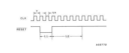
Hardware Reset Timing
| Item | Minimum | Maximum | Unit | |
|---|---|---|---|---|
| t1 | Reset signal pulse width | 2T | ns | |
| t2 | LSI access disabled time | 5T | ns | |
| T | Clock period | 60 | ns |
This catalog provides information as of December, 1997. Specifications and information herein are subject to change without notice.
No. 4909-13/13