
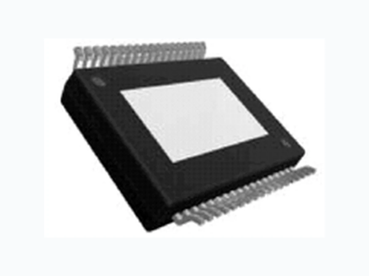
Door actuator driver
Document overview
- Manufacturer or author: STMICROELECTRONICS
- PDF pages: 39
Technical content
Datasheet sections
- 1 Block diagram and pin description
- 2 Electrical specifications
- 2.1 Absolute maximum ratings
- 2.2 ESD protection
- 2.3 Thermal data
- 2.4 Temperature warning and thermal shutdown
- 2.5 Electrical characteristics
- 2.6 SPI - electrical characteristics
- 3 Application information
- 3.1 Dual power supply: VS and VCC
- 3.2 Standby mode
- 3.3 Inductive loads
- 3.4 Diagnostic functions
- 3.5 Overvoltage and under voltage detection
- 3.6 Temperature warning and thermal shutdown
- 3.7 Open-load detection
- 3.8 Over load detection
- 3.9 Current monitor
- 3.10 PWM inputs
- 3.11 Cross current protection
- 4 Functional description of the SPI
- 4.1 Serial Peripheral Interface (SPI)
- 4.2 Chip Select Not (CSN)
- 4.3 Serial Data In (DI)
- 4.4 Serial Data Out (DO)
- 4.5 Serial clock (CLK)
- 4.6 Input data register
Features
■ One full bridge for 6A load (Ron=150 m ) ■ Two half bridges for 3A load (Ron=300 m ) ■ Two half bridges for 1.5A load (Ron=800 m ) ■ One highside driver for 6A load (Ron=100 m ) ■ Four highside drivers for 1.5 A load (Ron=800 m ) ■ Programmable softstart function to drive loads with higher inrush currents (i.e. current >6 A,>3 A,>1.5 A) ■ Very low current consumption in standby mode S < 6 A typ; ICC <25 A typ; Tj 85 °C) ■ All outputs short circuit protected ■ Current monitor output for 300 m, 150 m and 100 m highside drivers ■ All outputs over temperature protected ■ Open load diagnostic for all outputs ■ Overload diagnostic for all outputs ■ Seperated half bridges for door lock motor ■ PWM control of all outputs ■ Charge pump output for reverse polarity protection
Applications
■ Door actuator driver with bridges for door lock and safe lock, mirror axis control, mirror fold and highside driver for mirror defroster and four 10W-light bulbs.
Description
The L9950 and L9950XP are microcontroller driven multifunctional door actuator driver for automotive applications.Up to five DC motors and five grounded resistive loads can be driven with six half bridges and five highside drivers. The integrated standard serial peripheral interface (SPI) controls all operation modes (forward, reverse, brake and high impedance). All diagnostic informations are available via SPI. PowerSO-36 PowerSSO-36 Table 1. Device summary
1 Block diagram and pin description
Figure 1. Block diagram Table 2. Pin definitions and functions pins of GND must be externally connected. pins of OUT11 must be externally connected.
GND to output). This output is over-current and open load protected. Power supply voltage (external reverse protection required. pins of VS must be externally connected. significant bit (LSB, bit 0) is transferred first.
9 CM/PWM2
Current monitor output/PWM2 input.
10 CSN
Chip select not input/test mode. to CSN pin the L9950 will be switched into a test mode.
12 VCC
13 CLK
Half bridge output 4,5,6: see OUT1 (pin 3). pins of OUT4 (OUT5, respectively) must be externally connected. Table 2. Pin definitions and functions (continued)
Figure 2. Configuration diagram (top view)
27 PWM1
OUT11 by an external PWM signal. Highside driver output 7,8,9,10.
31 OUT8
2 Electrical specifications
2.1 Absolute maximum ratings
Program and other relevant quality document.
2.2 ESD protection
2.3 Thermal data
Table 3. Absolute maximum ratings Table 4. ESD protection
- HBM according to CDF-AEC-Q100-002.
- HBM with all unzapped pins grounded.
Table 5. Thermal data
2.4 Temperature warning and thermal shutdown
2.5 Electrical characteristics
VS = 8 to 16 V, VCC = 4.5 to 5.3 V, Tj = - 40 to 150 °C, unless otherwise specified. Table 6. Temperature warning and thermal shutdown Table 7. Supply
Table 8. Overvoltage and under voltage detection Table 9. Current monitor output Table 10. Charge pump output
Table 11. OUT1 - OUT11
Table 11. OUT1 - OUT11 (continued)
2.6 SPI - electrical characteristics
Note: Value of input capacity is not measured in production test. Parameter guaranteed by design. Table 12. Delay time from standby to active mode Switching from standby to active mode. Table 13. Inputs: CSN, CLK, PWM1/2 and DI
Tj=-40 °C/+25 °C: SPI communication @2 MHZ. Tj=+125 °C: SPI communication @1.25 MHZ. Table 14. DI timing Table 15. DO
- Value of input capacity is not measured in production test. Parameter guaranteed by design.
Figure 3. SPI - transfer timing diagram Table 16. DO timing Table 17. CSN timing
Figure 4. SPI - input timing Figure 5. SPI - DO valid data delay time and valid time
0.8 VCC
0.2 VCC
0.5 VCC
Figure 6. SPI - DO enable and disable time Figure 7. SPI - driver turn-on/off timing, minimum csn hi time
Figure 8. SPI - timing of st atus bit 0 (fault condition)
Application information L9950 - L9950XP 20/39 Doc ID 10311 Rev 11
3 Application information
3.1 Dual power supply: V S and VCC
The power supply voltage VS supplies the half bridges and the highside drivers. An internal charge-pump is used to drive the highside switches. The logic supply voltage VCC (stabilized 5 V) is used for the logic part and the SPI of the device. Due to the independent logic supply voltage the control and status information will not be lost, if there are temporary spikes or glitches on the power supply voltage. In case of power- on (V CC increases from under voltage to VPOR OFF = 4.2 V) the circuit is initialized by an internally generated power on reset (POR). If the voltage VCC decreases under the minimum threshold (VPOR ON = 3.4 V), the outputs are switched to tristate (high impedance) and the status registers are cleared.
3.2 Standby mode
The standby mode of the L9950 is activated by clearing the bit 23 of the Input Data Register 0. All latched data will be cleared and the inputs and outputs are switched to high impedance. In the standby mode the current at V S (VCC) is less than 6 µA (50 µA) for CSN = high (DO in tristate). By switching the VCC voltage a very low quiescent current can be achieved. If bit 23 is set, the device will be switched to active mode.
3.3 Inductive loads
Each half bridge is built by an internally connected highside and a lowside power DMOS transistor. Due to the built-in reverse diodes of the output transistors, inductive loads can be driven at the outputs OUT1 to OUT6 without external free wheeling diodes. The highside drivers OUT7 to OUT11 are intended to drive resistive loads. Hence only a limited energy (E<1 mJ) can be dissipated by the internal ESD diodes in freewheeling condition. For inductive loads (L>100 µH) an external free wheeling diode connected to GND and the corresponding output is needed.
3.4 Diagnostic functions
All diagnostic functions (over/open load, power supply over-/undervoltage, temperature warning and thermal shutdown) are internally filtered and the condition has to be valid for at least 32 µs (open load: 1 ms, respectively) before the corresponding status bit in the status registers will be set. The filters are used to improve the noise immunity of the device. Open load and temperature warning function are intended for information purpose and will not change the state of the output drivers. On contrary, the overload and thermal shutdown condition will disable the corresponding driver (overload) or all drivers (thermal shutdown), respectively. Without setting the over-current recovery bits in the Input Data register, the microcontroller has to clear the over-current status bits to reactivate the corresponding drivers.
3.5 Overvoltage and un der voltage detection
If the power supply voltage VS rises above the overvoltage threshold VSOV OFF (typical 21 V), the outputs OUT1 to OUT11 are switched to high impedance state to protect the load. When the voltage V S drops below the under voltage threshold VSUV OFF (UV switch OFF voltage), the output stages are switched to the high impedance to avoid the operation of the power devices without sufficient gate driving voltage (increased power dissipation). If the supply voltage V S recovers to normal operating voltage the outputs stages return to the programmed state (input register 0: bit 20=0). If the under voltage/overvoltage recovery disable bit is set, the automatic turn-on of the drivers is deactivated. The microcontroller needs to clear the status bits to reactivate the drivers. It is recommended to set bit 20 to avoid a possible high current oscillation in case of a shorted output to GND and low battery voltage.
3.6 Temperature warning and thermal shutdown
If junction temperature rises above Tj TW a temperature warning flag is set and is detectable via the SPI. If junction temperature increases above the second threshold Tj SD, the thermal shutdown bit will be set and power DMOS transistors of all output stages are switched off to protect the device. In order to reactivate the output stages the junction temperature must decrease below T j SD - Tj SD HYS and the thermal shutdown bit has to be cleared by the microcontroller.
3.7 Open-load detection
The open load detection monitors the load current in each activated output stage. If the load current is below the open load detection threshold for at least 1 ms (t dOL) the corresponding open load bit is set in the status register. Due to mechanical/electrical inertia of typical loads a short activation of the outputs (e.g. 3ms) can be used to test the open load status without changing the mechanical/electrical state of the loads.
3.8 Over load detection
In case of an over-current condition a flag is set in the status register in the same way as open load detection. If the over-current signal is valid for at least t ISC = 32 µs, the over- current flag is set and the corresponding driver is switched off to reduce the power dissipation and to protect the integrated circuit. If the over-current recovery bit of the output is zero the microcontroller has to clear the status bits to reactivate the corresponding driver.
Application information L9950 - L9950XP 22/39 Doc ID 10311 Rev 11
3.9 Current monitor
The current monitor output sources a current image at the current monitor output which has a fixed ratio (1/10000) of the instantaneous current of the selected highside driver. The bits 18 and 19 of the Input Data Register 0 control which of the outputs OUT1, OUT4, OUT5, OUT6 and OUT11 will be multiplexed to the current monitor output. The current monitor output allows a more precise analysis of the actual state of the load rather than the detection of an open or overload condition. For example this can be used to detect the motor state (starting, free running, stalled). Moreover, it is possible to regulate the power of the defroster more precise by measuring the load current. The current monitor output is bidirectional (c.f. PWM inputs).
3.10 PWM inputs
Each driver has a corresponding PWM enable bit which can be programmed by the SPI interface. If the PWM enable bit is set, the output is controlled by the logically AND combination of the PWM signal and the output control bit in Input Data Register. The outputs OUT1-OUT8 and OUT11 are controlled by the PWM1 input and the outputs OUT9/10 are controlled by the bidirectional input CM/PMW2. For example, the two PWM inputs can be used to dim two lamps independently by external PWM signals.
3.11 Cross current protection
The six half brides of the device are cross current protected by an internal delay time. If one driver (LS or HS) is turned off the activation of the other driver of the same half bridge will be automatically delayed by the cross current protection time. After the cross current protection time is expired the slew rate limited switch off phase of the driver will be changed to a fast turn-off phase and the opposite driver is turned on with slew rate limitation. Due to this behavior it is always guaranteed that the previously activated driver is totally turned off before the opposite driver will start to conduct.
3.12 Programmable soft start function to drive loads with higher
Loads with start-up currents higher than the over-current limits (e.g. inrush current of lamps, start current of motors and cold resistance of heaters) can be driven by using the programmable soft start function (i.e. overcurrent recovery mode). Each driver has a corresponding over-current recovery bit. If this bit is set, the device will automatically switch- on the outputs again after a programmable recovery time. The duty cycle in over-current condition can be programmed by the SPI interface to be about 12% or 25%. The PWM modulated current will provide sufficient average current to power up the load (e.g. heat up the bulb) until the load reaches operating condition. The device itself cannot distinguish between a real overload and a non linear load like a light bulb. A real overload condition can only be qualified by time. As an example the microcontroller can switch on light bulbs by setting the over-current Recovery bit for the first 50ms. After clearing the recovery bit the output will be automatically disabled if the overload condition still exits.
Figure 9. Example of programmable soft start function for inductive loads
Functional description of the SPI L9950 - L9950XP 24/39 Doc ID 10311 Rev 11
4 Functional description of the SPI
4.1 Serial Peripheral Interface (SPI)
This device uses a standard SPI to communicate with a microcontroller. The SPI can be driven by a microcontroller with its SPI peripheral running in following mode: CPOL = 0 and CPHA = 0. For this mode, input data is sampled by the low to high transition of the clock CLK, and output data is changed from the high to low transition of CLK. This device is not limited to microcontroller with a build-in SPI. Only three CMOS-compatible output pins and one input pin will be needed to communicate with the device. A fault condition can be detected by setting CSN to low. If CSN = 0, the DO pin will reflect the status bit 0 (fault condition) of the device which is a logical or of all bits in the status registers 0 and 1. The microcontroller can poll the status of the device without the need of a full SPI communication cycle. Note: In contrast to the SPI st andard the least significant bit (LSB) will be transferred first (see Figure 3).
4.2 Chip Select Not (CSN)
The input pin is used to select the serial interface of this device. When CSN is high, the output pin (DO) will be in high impedance state. A low signal will activate the output driver and a serial communication can be started. The state when CSN is going low until the rising edge of CSN will be called a communication frame. If the CSN input pin is driven above 7.5V, the L9950 will go into a test mode. In the test mode the DO will go from tri state to active mode.
4.3 Serial Data In (DI)
The input pin is used to transfer data serial into the device. The data applied to the DI will be sampled at the rising edge of the CLK signal and shifted into an internal 24 bit shift register. At the rising edge of the CSN signal the contents of the shift register will be transferred to Data Input Register. The writing to the selected Data Input Register is only enabled if exactly 24 bits are transmitted within one communication frame (i.e. CSN low). If more or less clock pulses are counted within one frame the complete frame will be ignored. This safety function is implemented to avoid an activation of the output stages by a wrong communication frame. Note: Due to this safety functionality a daisy chai ning of SPI is not possible. Instead, a parallel operation of the SPI bus by controlling the CSN signal of the connected ICs is recommended.
L9950 - L9950XP Functional description of the SPI Doc ID 10311 Rev 11 25/39
4.4 Serial Data Out (DO)
The data output driver is activated by a logical low level at the CSN input and will go from high impedance to a low or high level depending on the status bit 0 (fault condition). The first rising edge of the CLK input after a high to low transition of the CSN pin will transfer the content of the selected status register into the data out shift register. Each subsequent falling edge of the CLK will shift the next bit out.
4.5 Serial clock (CLK)
The CLK input is used to synchronize the input and output serial bit streams. The data input (DI) is sampled at the rising edge of the CLK and the data output (DO) will change with the falling edge of the CLK signal.
4.6 Input data register
The device has two input registers. The first bit (bit 0) at the DI input is used to select one of the two Input Registers. All bits are first shifted into an input shift register. After the rising edge of CSN the contents of the input shift register will be written to the selected Input Data Register only if a frame of exact 24 data bits are detected. Depending on bit 0 the contents of the selected status register will be transferred to DO during the current communication frame. Bit 1-17 controls the behavior of the corresponding driver. If bit 23 is zero, the device will go into the standby mode. The bits 18 and 19 are used to control the current monitor multiplexer. Bit 22 is used to reset all status bits in both status registers. The bits in the status registers will be cleared after the current communication frame (rising edge of CSN).
4.7 Status register
This devices uses two status registers to store and to monitor the state of the device. Bit 0 is used as a fault bit and is a logical NOR combination of bits 1-22 in both status registers. The state of this bit can be polled by the microcontroller without the need of a full SPI communication cycle. If one of the over-current bits is set, the corresponding driver will be disabled. If the over-current recovery bit of the output is not set the microcontroller has to clear the over-current bit to enable the driver. If the thermal shutdown bit is set, all drivers will go into a high impedance state. Again the microcontroller has to clear the bit to enable the drivers.
4.8 Test mode
available to measure the internal bandgap voltage, the TW and TSD thresholds. Table 18. Test mode
Table 19. SPI - input data and status registers 0
23 Enable bit
22 Reset bit
18 Current monitor
18 Output
(e.g. measuring filter times).
10 OUT1/OUT
01 O U T 5
11 O U T 4
17 OUT11 – HS
16 OUT10 – HS
15 OUT9 – HS
14 OUT8 – HS
13 OUT7 – HS
12 OUT6 – HS
11 OUT6 – LS
10 OUT5 – HS
9 OUT5 – LS
8 OUT4 – HS
7 OUT4 – LS
6 OUT3 – HS
5 OUT3 – LS
4 OUT2 – HS
3 OUT2 – LS
2 OUT1 – HS
1 OUT1 – LS
Table 19. SPI - input data and status registers 0 (continued)
Table 20. SPI - input data and status registers 1 will be switched in active mode. and the output is switched off. 21 of Input Data Register 0). even if this bit is set to zero.
11 OUT11 PWM1
are controlled by PWM1 input.
10 OUT10 PWM2
9 OUT9 PWM2
8 OUT8 PWM1
7 OUT7 PWM1
6 OUT6 PWM1
5 OUT4 PWM1
4 OUT4 PWM1
3 OUT3 PWM1
2 OUT4 PWM1
1 OUT4 PWM1
Table 20. SPI - input data and status registers 1 (continued)
5 Packages thermal data
Figure 10. Packages thermal data
6 Package and packing information
6.1 ECOPACK ®
specifications, grade definitions and product status are available at: www.st.com. ECOPACK® is an ST trademark.
6.2 PowerSO-36 package information
Figure 11. PowerSO-36 package dimensions
Table 21. PowerSO-36 mechanical data
6.3 PowerSSO-36 package information
Figure 12. PowerSSO-36 package dimensions Table 22. PowerSSO-36 mechanical data
6.4 PowerSO-36 packing information
Figure 13. PowerSO-36 tube shipment (no suffix)
- “D” and “E” do not include mold Flash or protrusions. Mold Flash or protrusions shall not exceed 0.15 mm
Table 22. PowerSSO-36 mechanical data (continued)
Figure 14. PowerSO-36 tape and reel shipment (suffix “TR”)
6.5 PowerSSO-36 packing information
Figure 15. PowerSSO-36 tube shipment (no suffix) Figure 16. PowerSSO-36 tape and reel shipment (suffix “TR”)
7 Revision history
Table 23. Document revision history Document restructured and reformatted. 05-Nov-2008 8 Updated Table 22: PowerSSO-36 mechanical data. 19-Sep-2013 11 Updated Disclaimer.