
Smart quad switch
Document overview
- Manufacturer or author: STMICROELECTRONICS
- PDF pages: 9
Technical content
■ Modified VDMOS Power Stage (UDSBR > 80V) ■ RDSON < 500 mOhm (Tj = 25°C) ■ CMOS Compatible Inputs ■ Enable Input (Reset) ■ Outputs Capable of up to 2.2 Amperes ■ Outputs Internally Clamped at 70V for Fast Inductive Load Switch Off ■ Wide operating supply voltage from 4.7V up to 30V ■ DIAGNOSTIC FUNCTIONS ■ Open Load Detection (Output off, 100s- filtering time) ■ Short to Ground Detection (Output off, 100s - filtering time) ■ Short to Battery Detection (Output on) ■ Over temperature detection (Output on) ■ Storage of last fault in 8 Bit - Serial Register ■ Fault Signal Indication at Serial Data Out without need to read out the Serial Interface ■ Daisy Chainable Serial Diagnostic ■ Serial Interface Clock Frequency up to 500kHz
DESCRIPTION
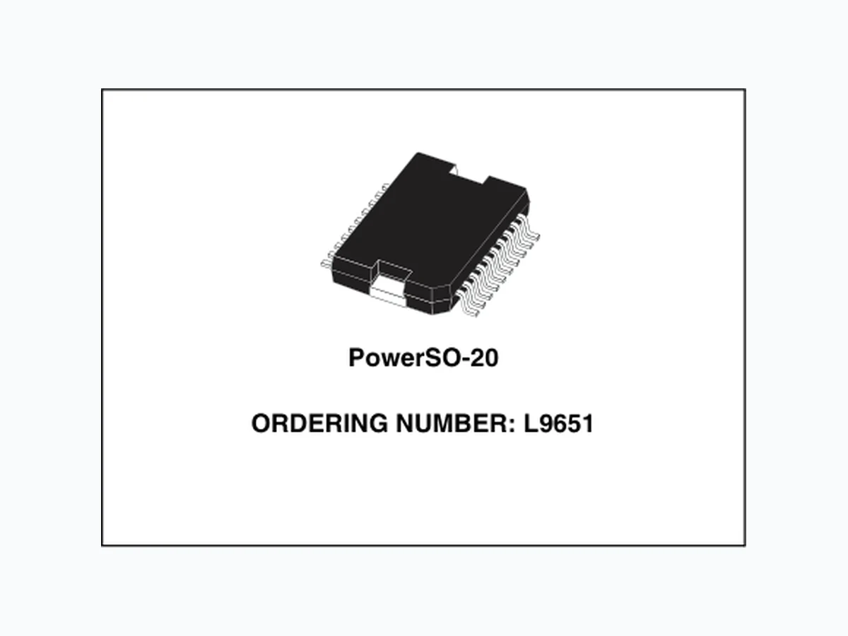
The L9651 consists of four identical low side power switches. A serial diagnostic interface indicates fail ure mode of each switch (short circuit to V BAT or ground and open load or over temperature). PowerSO-20 ORDERING NUMBER: L9651 SMART QUAD SWITCH BLOCK DIAGRAM Serial Diagnostic Tur n On VBAT Clock Sync. Serial Data Out Ground Reset Four Fold Logic Short Circuit Protection Fault Detection References Gate Control Output 1..4 Data In Inputs 1..4 Underv. Shutd.
PIN CONNECTION (Top view) PIN FUNCTION N° Pin Function 1, 10, 11, 20 GND Ground 2, 19 N.C. Not Connected
3 IN1 Input 1
4 IN2 Input 2
5 OUT1 Output 1
6 VBAT Supply Voltage
7 OUT2 Output 2
8 DO Serial Data Out
9 CL Clock
12 SY Synchronization
13 DI Serial Data In
14 OUT3 Output 3
15 R Reset
16 OUT4 Output 4
17 IN3 Input 3
18 IN4 Input 4
N.C. GND 10
11 GND
R IN3 N.C. GND IN4
ELECTRICAL CHARACTERISTCS (6.5V < VBAT < 25V, -40 < TJ < 150°C) Symbol Parameter Value Unit TSTG Storage Temperature -55 to 150 oC TJ Operating Junction Temperature -40 to 150 oC VBAT DC Supply Voltage -2 to 30 V VBATtr Transient Supply Voltage; t < 400ms 40 V VOUT Output Voltage 65 V VOUTtr Transient Output Voltage; during clamping 78 V ECL Output Clamping energy; repetition rate < 100 Hz 10 mJ -IOUT Output reverse current 2 A VR,VINi,VDI, VCLVSY Control Input voltage -0.3 to 6.5 V VDO Control Output voltage -0.3 to 6.5 V Symbol Parameter Value Unit Rth j-case Thermal Resistance Junction to Case 2.5 °C/W Symbol Parameter Test Condition Min. Typ. Max. Unit Supply Voltage VBATU Turn on threshold voltage 2.0 4.7 V IBAT Supply current VBAT = 14V VOUTi > 0V 4 10 15 mA Output stage RDSON On resistance VBAT = 14V TJ = 25°C; Iout = 1A VBAT = 14V TJ = 150°C; Iout = 1A 500 850 VCL Clamping voltage, inductive load Iout = 0.5 A 63 70 76 V IOUTi Over current shutdown (Shutdown latch resets with pos. slope at INi) TJ = -40°C TJ = 25°C TJ = 150°C 3.0 2.5 2.2 4.3 3.7 3.5 A A A Output leakage current see: Open load diagnostic current
Logic Inputs IN1...IN4, SY , CL, DI, R VINiLH VSYLH VCLLH VRLH VDILH Input High level 3.5 6.5 V VINiHL VSYHL VCLHL VRHL VDIHL Input Low level -0.3 1.5 V VINih VSYh VCLh VRh VDIh Hysteresis 0.2 1 V - IINi - ISY - IC L - IR Input current IN1 ... IN4, SY , CL, R (Internal pull up current source) VINi = 0V 10 40 120 A VSY = 0V VCL = 0V VR = 0V 10 80 - IDI Input current DI (Internal pull up current source) VDI = 0V 120 220 250 A Timing tdon Turn on delay 7.5 s tdoff Turn off delay 7.5 s son Switch on slew rate 10 V/s soff Switch off slew rate 15 V/s toc Over current detection time 0.5 s tv Open load filtering time 60 100 200 s tv Short to GND filtering time 60 100 200 s fCL Serial clock frequency 0 500 kHz tvDV DO: Datavalidtime 0.03 1 s tvset DI: Datasettlingtime 0.5 s tvhold DI: Dataholdtime 0 s Diagnostic VBATDU Under voltage threshold 4.7 7.5 V Serial Data output (External pull up required) VDO Data output low voltage IDO < 1.6mA 7.5V < VBAT < 22V 0 0.45 V | IDO | Data output leakage current 10 A Symbol Parameter Test Condition Min. Typ. Max. Unit ELECTRICAL CHARACTERISTCS (continued)
Figure 1. Typical Timing Diagram for Serial Diagnostic Fault: Short to Battery or over temp.
Figure 4. Application Circuit
- ●● ● RR R
5 Volt
e a2 A E PSO20MEC DETAIL A T D 11 0 1120 E1E2 h x 45˚ DETAIL Alead sluga3 S Gage Plane 0.35 L DETAIL B R DETAIL B (COPLANARITY) GC - C - SEATING PLANE b c NN H BOTTOM VIEW DIM. mm inch A3 . 6 0 . 1 4 2 a1 0.1 0.3 0.004 0.012 a2 3.3 0.130 a3 0 0.1 0.000 0.004 b 0.4 0.53 0.016 0.021 c 0.23 0.32 0.009 0.013 D (1) 15.8 16 0.622 0.630 D1 (2) 9.4 9.8 0.370 0.386 E 13.9 14.5 0.547 0.570 e 1.27 0.050 e3 11.43 0.450 E1 (1) 10.9 11.1 0.429 0.437 E2 2.9 0.114 E3 5.8 6.2 0.228 0.244 G 0 0.1 0.000 0.004 H 15.5 15.9 0.610 0.626 h 1.1 0.043 L 0.8 1.1 0.031 0.043 N 8˚(typ.) S 8˚(max. ) T 10 0.394 (1) “D and E1” do not include mold flash or protusions. - Mold flash or protusions shall not exceed 0.15mm (0.006”) - Critical dimensions: “E”, “G” and “a3”. (2) For subcontractors, the limit is the one quoted in jedec MO-166 PowerSO-20 0056635 I JEDEC MO-166 Weight: 1.9gr