

 Download PDF
Quad low side driver
Document overview
- Manufacturer or author: STMICROELECTRONICS
- PDF pages: 14
Technical content
Datasheet sections
- 1 Block diagram
- 2 Pins description
- 3 Electrical specifications
- 3.1 Absolute maximum ratings
- 3.2 Thermal data
- 3.3 Operating condition
- 3.4 Electrical characteristics
- 4 Circuit description
- 5 Package information
- 6 Revision history
Features
■ Wide input voltage range from -24 V up to +45 V ■ Wide operating supply voltage range from
4.5 V up to 32 V
■ Reverse biasing protected (VS = -24 V) ■ Very low standby quiescent current < 2 µA ■ Programmable signal transfer polarity ■ TTL and CMOS compatible inputs ■ Defined output off state off for open inputs ■ Three open drain DMOS outputs, with RDSon =1 . 5 . at 25 °C and VS > 6 V ■ Output current limitation ■ Controlled output slope for low EMI ■ Over temperature shut-down ■ Integrated output clamping for fast inductive recirculation VFB > 45 V ■ Status monitoring for: – Over temperature – Disconnected ground or supply voltage ■ ESD: all pins are guaranteed till 2 kV human body mode
Description
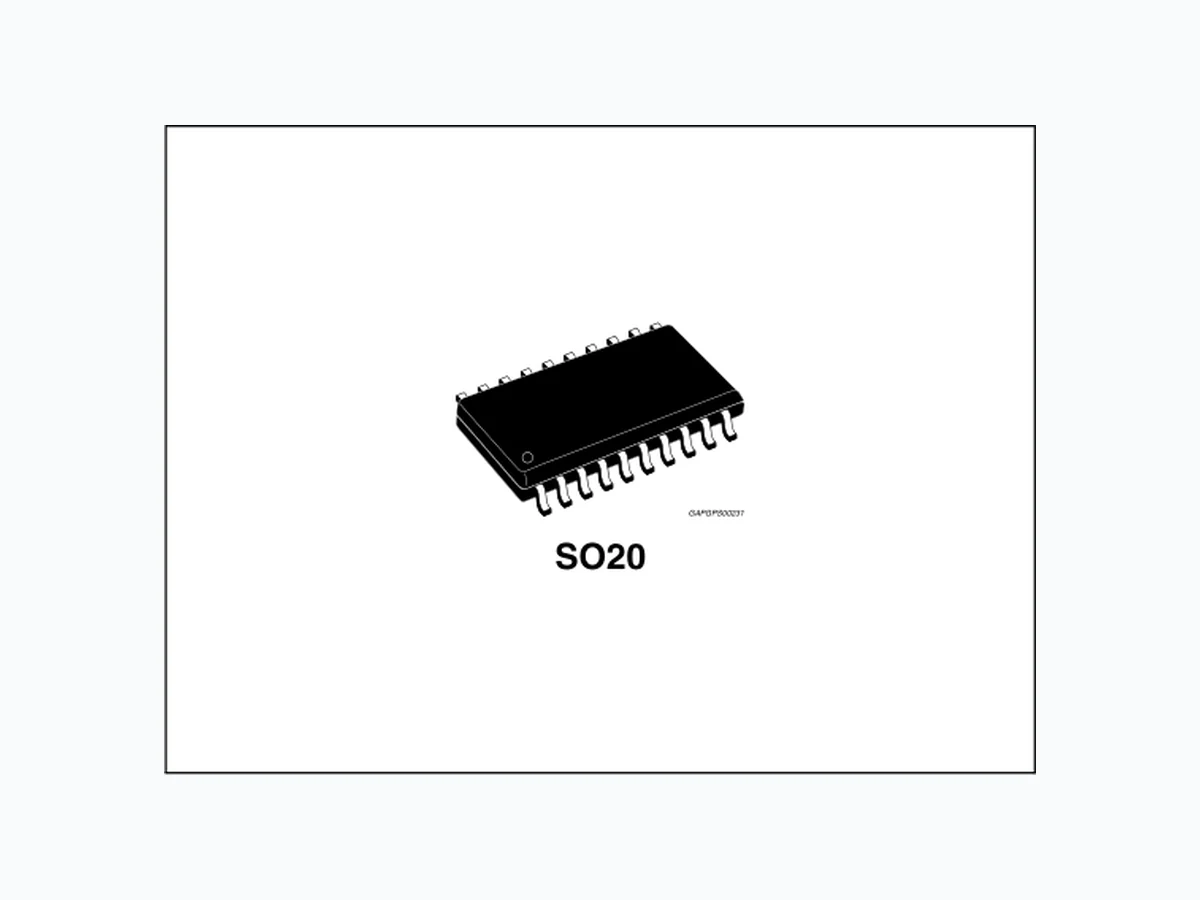
The L9338 is a monolithic integrated quad low side driver realized in advanced Multipower-BCD technology. It is intended to drive lines, lamps or relays in automotive or industrial applications. '!0'03 SO20 Table 1. Device summary
1 Block diagram
Figure 1. Block diagram
2 Pins description
Figure 2. Pins connection diagram Table 2. Pins function
1 IN1 Input 1
2 IN2 Input 2
3 DIAG Diagnostic
8 VS Supply voltage
9 IN3 Input 3
10 IN4 Input 4
11 EN Enable
12 OUT 4 Output 4
13 OUT 3 Output 3
18 OUT 2 Output 2
19 OUT 1 Output 1
20 PRG Program
3 Electrical specifications
3.1 Absolute maximum ratings
3.2 Thermal data
3.3 Operating condition
otherwise specified. The function will be guaranteed by design until TjMON switch-OFF-level. Table 3. Absolute maximum ratings (no damage or latch) Table 4. Thermal data Table 5. Operating condition
3.4 Electrical characteristics
Table 6. Electrical characteristics
Figure 3. Timing diagram
4 Circuit description
internally fixed at low status by open input condition. Each output driver has a current limitation of min. 0.4 A and a separate thermal shut-down. The thermal shut-down deactivates that output which exceeds temperature switch off level. of parasitic inside the power DMOS. and switched on at over temperature. Table 7. Diagnostic
- Selective for each channel at over temperature.
Figure 4. Application circuit for inverting transfer polarity
5 Package information
specifications, grade definitions and product status are available at: www.st.com. ECOPACK® is an ST trademark. Figure 5. SO20 mechanical data and package dimensions
6 Revision history
Table 8. Document revision history