
L9001 STM
Document overview
- Manufacturer or author: Provided By www.digicamel.com(FREE DATASHEET DOWNLOAD SITE)
- PDF pages: 38
Technical content
Datasheet sections
- 1 General description
- 1.1 VDD1 regulator
- 1.2 VDD2 regulator
- 1.3 ADCLDO regulator
- 1.4 Supervision and diagnosis
- 1.5 Low power mode
- 2 Block and application diagrams
- 3 Pin description
- 4 Electrical specifications
- 4.1 Absolute maximum ratings
- 4.2 ESD protection
- 4.3 Operating range
- 4.4 Thermal data
- 4.5 General operating conditions
- 5 Power supply
- 5.1 Configuration
- 5.2 VDD1 regulator
- 5.3 VDD2 regulator
- 5.4 ADCLDO Regulator
- 5.5 Power up and power down sequences
- 6 Diagnosis
- 7 Watchdog
- 8 Operation modes
- 8.1 Operation modes condition
- 8.2 Description of the operation modes
- 8.2.1 OFF mode
Features
AEC-Q100 qualified Flexible, configurable voltage regulator for multiple power supply schemes – First stage asynchronous switch mode regulator (VDD1), supplying second stage regulator (VDD2), peripherals or μC [3.3 V/5.0 V/6.0 V/1 A]; optionally disabled – Second regulator (VDD2), configurable as BUCK converter or LDO regulator, supplying peripherals, μC or μC-core [0.8 V to 5.0 V/1 A BUCK and 300 mA for LDO]; optionally disabled – ADC LDO [3.3 V/5 V/100 mA] for ADC μC supply Supervision and diagnosis – VS monitoring – Over temperature detection – Output supply supervision – Output overcurrent protection Fail-safe functionality – Output under or over voltage reset generation – Configurable Watchdog – Over temperature shutdown Low power mode
Description
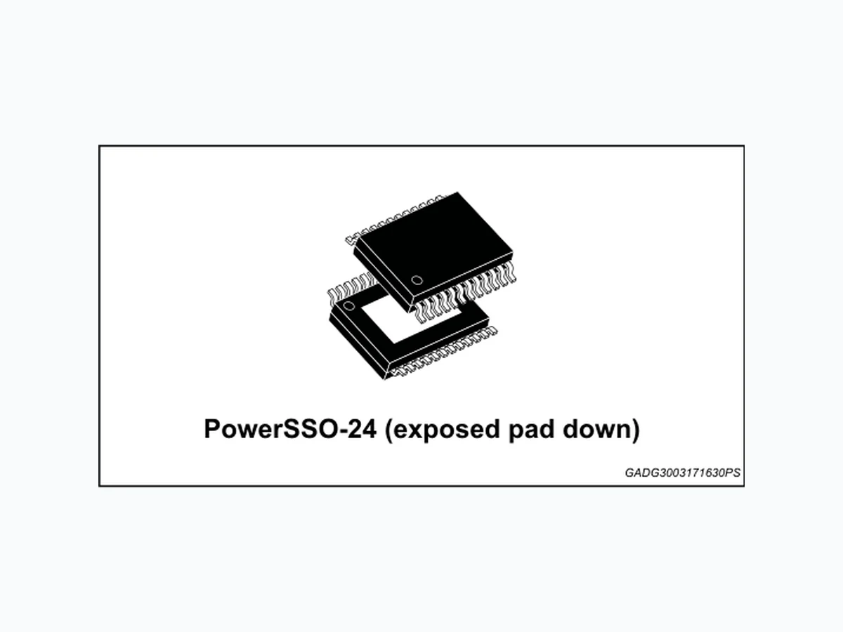
L9001 SPS (Simple Power Supply) device is a multiple power regulator for Automotive applications with one buck regulator, one configurable buck or linear regulator and one linear regulator. Its output voltages are configurable via discrete pins. On top of the regulators, this device integrates a watchdog functional block, and a diagnosis functional block (under/over voltage, output current and temperature). Device is capable of low power operation mode with main regulators still active and reduced power consumption from battery. 3RZHU662 H[SRVHGSDGGRZQ *$'*36 Table 1. Device summary
- The exposed pad dimensions for this device is
1 General description
The L9001 is a power management device targeting various automotive applications. The device contains three voltage regulators: VDD1, VDD2 and ADCLDO.
1.1 VDD1 regulator
VDD1 is an asynchronous switch mode power supply with integrated FET and can be used as pre-regulator for VDD2 and/or to supply external devices such as μC, transceivers, or sensors. The regulated voltage can be configured to 3.3 V / 5 V or 6 V by a proper connection of CONF3 input pin. Current capability is up to 1A, and the device provides an internal peak current limitation as protection. In addition VDD1 output voltage is monitored through VR1 pin and if the voltage goes outside the specified range, RSTN1 output is asserted low; when the fault disappears the output is released after the specified hold time. If the application does not require it, VDD1 regulator can be also disabled without the need to insert additional external components.
1.2 VDD2 regulator
VDD2 is a configurable power supply with integrated FET that can be used as BUCK regulator (also referenced as BUCK2 in this case) or as LDO regulator (also referenced as LDO2 in this case) to supply μC or μC core. In fact the regulated voltage is highly configurable and can be adjusted between 0.8 V and 5 V by proper sizing of external divider on FB2 input pin. The choice between BUCK and LDO is done by setting the proper connection of CONF2 input pin. Current capability is up to 1 A in BUCK mode and 300 mA in LDO mode and the device provides an internal limitation according to the chosen option (BUCK / LDO). In addition VDD2 output voltage is monitored through FB2 input pin and if the voltage goes outside the specified range, RSTN2 output is asserted low; when the fault disappears the output is released after the specified hold time. The input voltage of VDD2 regulator can be connected to: VS supply voltage, in a configuration in which VDD2 is directly supplied from battery VDD1 output, in a configuration where VDD2 is supplied by VDD1 pre regulator The connection to VS battery will automatically disable VDD1 as the device does not allow the independent operation of VDD1 and VDD2 both supplied from battery. If the application does not require it, VDD2 regulator can be disabled without the need to insert additional external components.
1.3 ADCLDO regulator
ADCLDO is a LDO power supply with integrated FET which can be used for external loads with low current demand. The regulated voltage VADC can be configured to 3.3 V / 5 V by a proper connection of CONF1 input pin. Current capability is up to 100 mA, and the device provides an internal current limitation as protection. In addition VADC output voltage is monitored internally and if the voltage goes outside the specified range, ADCMON output is asserted low; when the fault disappears the output is released after the specified hold time.
1.4 Supervision and diagnosis
In addition to the described protection features of current limitation and output voltage monitor, the device provides additional supervision and diagnosis functions: VS UV/OV, over temperature, watchdog and latch mode. VS input voltage is monitored and if an undervoltage or overvoltage is detected with respect to the specified thresholds, the device enters a so called safe state in which output voltages are switched off. The device internal temperature is also monitored: when temperature increases over the specified threshold, the TWN output is asserted low and, if the temperature increases above a shutdown threshold, the device enters safe state. The device also has a charge pump block which is used to ensure proper regulators functionality inside spec limits; undervoltage on CP also triggers device safe state. The device integrates a watchdog functional block which constantly monitors the status of the microcontroller's oscillator. This is done by checking the synchronization of the microcontroller with an internal time signal whose period is configured by applying a specific capacitor at the input pin WDT. If the microcontroller signal, which is transmitted to the watchdog via the pin WDI, is not serving the watchdog correctly, the output pin WDO is asserted low for the specified time. L9001 provides a feature, called latch state, that disables the system in case a systematic fault is repetitively detected on the charge pump structure, watchdog or in case of repetitive thermal events. The separated fail counters and detection mechanism are explained in the dedicated sections of this document.
1.5 Low power mode
For low power applications L9001 provides a Low Power mode feature which drastically reduces the device power consumption while the attached loads are still supplied via bypass LDOs. This mode can be entered with STBY input pin to high level as described in the dedicated section of this document. Load current is monitored in this mode and main regulators are automatically reenabled if needed.
2 Block and application diagrams
Figure 1. Block diagram
Figure 2. Application diagram (VDD1 = 5 V, BUCK2 = 1.2, VADC = 3.3 V)
3 Pin description
Figure 3. Pin connection diagram (top view) Table 2. Pin out description
1 GND Power ground supply Global
2 ADCMON ADCLDO monitor (reset) O Local
3 RSTN1 VDD1 monitor (reset) O Local
4 RSTN2 VDD2 monitor (reset) O Local
5 VDDIO Input/Output voltage reference supply Local
6 CONF3 Configuration input 3 I Local
7 WAKE Wake-up input I Local
8 V1O VDD1 switching pin supply Local
9 VS Battery supply voltage supply Global
10 CP Charge pump output supply Local
11 CP2 Charge pump capacitor pin 2 supply Local
12 CP1 Charge pump capacitor pin 1 supply Local
13 V2O BUCK2 switching pin / LDO2 output voltage supply Local
14 VR1 VDD1 BYP output voltage / VDD2 supply pin supply Global
15 FB2 VDD2 feedback voltage pin I Local
16 VR2 VDD2 BYP output voltage supply Local
17 CONF1 Configuration input 1 I Local
18 CONF2 Configuration input 2 I Local
19 VADC ADCLDO output voltage supply Local
20 TWN Thermal warning output flag O Local
21 WDI Watchdog input I Local
22 STBY Stand-by input I Local
23 WDT Watchdog timer input I/O Local
24 WDO Watchdog error output flag O Local
Table 2. Pin out description (continued)
4 Electrical specifications
4.1 Absolute maximum ratings
4.2 ESD protection
Table 3. Absolute maximum ratings Table 4. ESD protection values
4.3 Operating range
4.4 Thermal data
4.5 General operating conditions
Table 5. Supply voltage range
- If VS<6.5V, VDD1 output degradation can occur depending on device settings (see VDD1 regulator section
Table 6. Thermal data
5 Power supply
5.1 Configuration
The device regulators must be configured by proper connection of CONFx input pins. VDD1 regulator output voltage level must be configured through pin CONF3. VDD2 regulator mode must be configured in either Buck regulator or LDO through pin CONF2. ADCLDO output voltage must be configured by proper configuration on pin CONF1. corresponding to each option are summarized in the table below. MID configuration (only for CONF3): pin CONF3 must be left open. be needed to refresh the signal values on the input pins.
5.2 VDD1 regulator
V / 5 V / 6 V as described in Section 5.1. Table 7. CONF3 configuration Table 8. CONF2 and CONF1 configuration
regulator for VDD2 in case VDD2 regulator is not disabled (see Section 5.3 for details). VR1 output pin to VS supply and CONF3 to ground. Table 9. VDD1 regulator parameters
1 A > Iload1 > ILIM_BP1
1 A > Iload1 > ILIM_BP1 ,
5.3 VDD2 regulator
current capability depends on the chosen option and is specified in Table 10. have the specified feedback reference voltage on the FB2 input pin. VDD1 output, in a configuration in which VDD2 is supplied by VDD1 pre regulator. the external load applicable on VDD1 is 1 A reduced by the input current of VDD2 regulator. V, whereas there are no limitations in LDO mode.
- For further load/line transient details, please refer to AN5163.
Table 9. VDD1 regulator parameters (continued)
Table 10. VDD2 regulator parameters
5.4 ADCLDO Regulator
voltage is VADC which can be selected as either 3.3 V or 5.0 V as described in Section 5.1.
5.5 Power up and power down sequences
define the start-up behavior. the VDD2 and ADCLDO regulators will start right after internal regulators are ready. minimum time of WPL, the internal regulators and all output pins are deactivated.
- For further load/line transient details, please refer to AN5163.
Table 10. VDD2 regulator parameters (continued) Table 11. ADCLDO regulator parameters
Figure 4. Power up and Power down sequences
Table 12. Wake parameters
6 Diagnosis
Each power supply line generated by the device is monitored against over voltage, under voltage and provides an internal current limitation circuit; besides the device provides additional diagnosis functions: watchdog, over temperature, VS UV/OV and latch mode. VDD1 regulator output is monitored through VR1 pin and if the voltage goes below (above) the specified threshold VR1_uv (VR1_ov) for more than t FILT_uv_VR1 (tFILT_ov_VR1) filter time, RSTN1 is driven low; when the fault disappears, RSTN1 is released after the specified time t RSTN1_act. VDD2 regulator output is monitored through FB2 pin and if the voltage goes below (above) the specified threshold VR2_uv (VR2_ov) for more than t FILT_uv_VR2 (tFILT_ov_VR2) filter time, RSTN2 is driven low; when the fault disappears, RSTN2 is released after the specified time t RSTN2_act. ADCLDO regulator output is monitored through VADC pin and if the voltage goes below (above) the specified threshold VADC_uv (VADC_ov) for more than tFILT_uv_VADC (tFILT_ov_VADC) filter time, ADCMON is driven low; when the fault disappears, ADCMON is released after the specified time tADCMON_act. As supervision watchdog function, the WDI input is monitored and WDO output is driven low in case of faults (see Section 7 for details) Internal junction temperature is monitored and when Tj > TW_H, TWN output is driven low and it is released when Tj < TW_L (hysteresis implemented); when T j > TSD, L9001 shut down regulators entering a protection mode called SAFE state (see Section 8.2.5 for details). L9001 goes back to ACTIVE mode when Tj < TW_L. TWN and WDO are open drain. RSTN1, RSTN2 and ADCMON all have an internal resistive pull-up R_INT_RPU to VDDIO. RSTN1, RSTN2 and ADCMON are driven low level at power-up when WAKE is greater than WAKE_Hth after WPH filter time and are released after their relative output voltages (VR1, VR2 and VADC) have risen above their under voltage thresholds. VS input pin is monitored and in case one of the following conditions applies the device goes in a protection mode called SAFE state: VS > VS_ov_h for a period longer than tFILT_VS_ov, – L9001 goes back to ACTIVE mode if VS < VS_ov_l for a period longer than tFILT_VS_ov VS < VS_uv_l for a period longer than tFILT_VS_uv, – L9001 goes back to ACTIVE mode if VS > VS_uv_h for a period longer than tFILT_VS_uv Internal CP voltage is monitored as well and when CP<CP_uv for a period longer than tFILT_CP_uv L9001 shuts down regulators and enters SAFE state; it goes back to ACTIVE mode if CP>CP_uv for a period longer than tFILT_CP_uv. L9001 provides a feature, called latch state, that disables the system in case a systematic fault is repetitively detected on CP_uv, watchdog or thermal shutdown events. For detailed description see LATCH mode description in Section 8.2.6.
Table 13. Diagnosis parameters
Table 13. Diagnosis parameters (continued)
7 Watchdog
of the watchdog control can be checked monitoring output pin WDO. is generated. It follows that more than one WDI toggle can occur in the time window. the device enters latch mode (see Section 8.2 and Figure 6 for details). regulators still function normally. Table 14. Watchdog parameters
Figure 5. Example of Watchdog functioning Table 14. Watchdog parameters (continued)
Figure 6. Watchdog flow diagram
8 Operation modes
8.1 Operation modes condition
8.2 Description of the operation modes
Figure 7; additional transitions details are given in and .
8.2.1 OFF mode
VS is greater than 5.5 V and WAKE is high, L9001 moves to ACTIVE mode.
8.2.2 ACTIVE mode
8.2.3 FLASH mode
Table 15. Operation modes description All output voltages are switched off.
8.2.4 LOW POWER mode
Low power mode corresponds to a state where the system needs to decrease the overall power consumption with a reduced level of functionality. In this state, ADCLDO is switched off, regulators VDD1 and VDD2 are working in bypass mode and Watchdog, over temperature, regulators over & under voltage are all disabled. The state can be entered by ACTIVE state by rising STBY pin. Depending on the active VDD regulators (i.e. the regulators which have not been disabled in the application), the low power mode is managed in a different way. When only VDD1 regulator is enabled and the STBY pin is asserted high, the device goes in LOW POWER mode if VR1 current is lower than ICMP1_l. In this case only the bypass LDO drives the wanted output voltage while the switch mode operation is deactivated. When VR1 current turns higher than ICMP1_h, the device goes back to ACTIVE mode. When only VDD2 regulator is enabled and the STBY pin is asserted high, the device goes in LOW POWER mode if VR2 current is lower than ICMP2_l. In this case only the bypass LDO drives the wanted output voltage. When VR2 current turns higher than ICMP2_h, the device goes back to ACTIVE mode. When both regulators are enabled and the STBY pin is asserted high and the total overall current generated by VDD1 regulator is lower than ICMP1_l, the device goes in LOW POWER mode and only the bypass LDOs drive the output voltages while the switch mode operation (or linear mode, depending on the configuration) is deactivated. When the total overall current turns higher than ICMP1_h, the device goes back to ACTIVE mode. For further details on transitions from and to low power mode please refer to AN5163.
8.2.5 SAFE mode
SAFE mode corresponds to a state that is entered automatically when a fail-safe triggering condition is generated in ACTIVE state. These failure conditions are four: over temperature shutdown, VS overvoltage, VS undervoltage, and charge pump undervoltage. When in SAFE mode, all output regulators and watchdog are switched off, monitoring and charge pump are still active. Exit from SAFE state occurs only if Failure condition disappears.
8.2.6 LATCH mode
LATCH mode corresponds to a state that is entered automatically when the system has persistent failures which are blocking the functionality and so it must be stopped or restarted. Thus the only way out of LATCH state is going to OFF state and then again in ACTIVE, otherwise the system will remain in LATCH state indefinitely. In LATCH state all output regulators and WD are switched off, monitoring and charge pump are also switched off, and WDO is low. In particular, the failures that can trigger LATCH state are: over temperature shutdown (OTSD), charge pump undervoltage (CP_UV) and watchdog fail. The IC has two separate failure counters: WD_FC which counts fails on watchdog; FC which counts fails on OTSD and CP_UV. Each time a failure is detected, the correspondent failure counter is incremented; LATCH mode occurs when either the FC failure counter or the WD_FC has reached a threshold of 4 failures.
When a watchdog failure is generated by the watchdog unit (see Section 7 for details) the counter WD_FC is incremented by 1. WD_FC is reset if the watchdog is correctly served or when the device is in OFF or FLASH or LOW POWER mode. It means that if there are 4 consecutive watchdog failures, WD_FC reaches a value of 4 and as a consequence the system goes in LATCH mode. While for WD_FC the failures must be consecutive to trigger LATCH state, for OTSD or CP_UV fails, a so called Refresh failure counter is implemented to filter out sporadic / not persistent failures triggering FC counter. When OTSD or CP_UV fails are detected, L9001 enters SAFE state (see Section 6 for details) and FC counter is incremented. Once the Failure condition disappears the system goes back to ACTIVE state, the power-up sequence for each regulator is launched, and Refresh Failure counter is started. If a FC trigger condition is detected again within 100 ms (30 s if previous failure was OTSD), the system goes again in SAFE state and FC counter is again incremented. Otherwise, if no Failure is detected in ACTIVE state within 100 ms (30 s if previous failure was OTSD), the FC counter is reset. A table to clarify transitions from and to SAFE mode and the refresh failure counter is also included in .
Figure 7. Operation modes state diagram
8.2.7 Operation modes parameters
Table 16. Consumption parameters Table 17. STBY pin parameters Table 18. Charge pump capacitors
9 Package information
specifications, grade definitions and product status are available at: www.st.com. ECOPACK® is an ST trademark.
9.1 PowerSSO-24 (exposed pad) package information
Figure 8. PowerSSO-24 (exposed pad) package outline
Table 19. PowerSSO-24 (exposed pad) package mechanical data
- Values in inches are converted from mm and rounded to 4 decimal digits.
- Dimensions D and E1 do not include mold flash or protrusions. Allowable mold flash or protrusions is ‘0.25
Table 19. PowerSSO-24 (exposed pad) package mechanical data (continued)
state indicating the next state and the behavior of FC, Refresh FC counter and thresholds. Table 20. Clarify transitions from and to ACTIVE mode
indicating the next state and the behavior of FC, Refresh FC counter and thresholds. Table 21. Clarify transitions from and to SAFE mode
Revision history
Table 22. Document revision history 13-Dec-2017 1 Initial release. – Section 8.2.4: LOW POWER mode on page 28 .