

 Download PDF
L8013 HAMAMATSU
Document overview
- PDF pages: 2
Technical content
Page 1
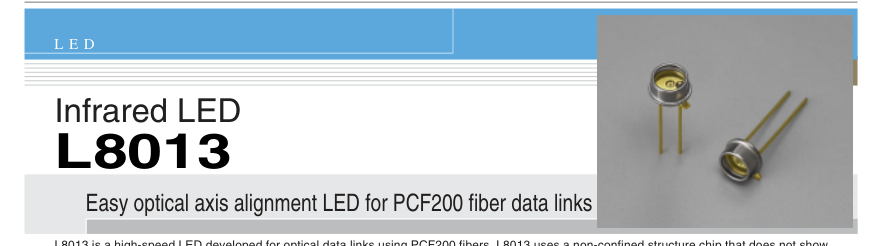
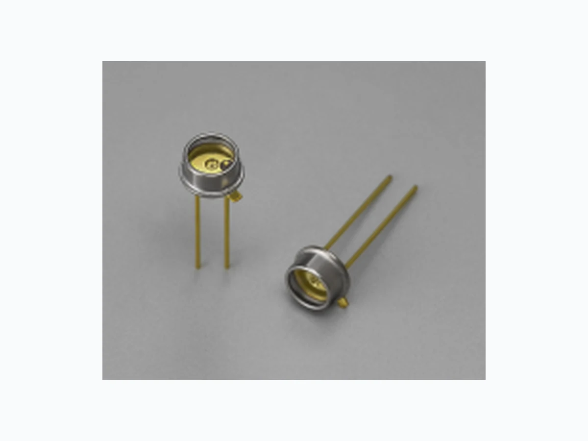
L8013 is a high-speed LED developed for optical data links using PCF200 fibers. L8013 uses a non-confined structure chip that does not show the abrupt deterioration often encountered in some types of confined chips, thus providing high reliability over extended operation time. The optical output at the fiber end usually tends to vary due to non-uniform LED chip thickness. L8013 minimizes this problem by using a light condensing reflector with a slight matching offset from the chip. This widens the fiber input beam profile so fine adjustment of the optical axis is not required.

(IF=30 mA, when used with PCF200 fiber) l High reliability
I Absolute maximum ratings (Ta=25 °C, unless otherwise noted)
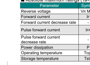
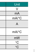
| Symbol | Condition | Value |
|---|---|---|
| VR Max. | 3 | |
| IF | 80 | |
| - | Ta > 25 °C | 1 |
| IFP | Pulse width=10 µs Duty ratio=1 % | 0.5 |
| - | Ta > 25 °C | 6.5 |
| P | 150 | |
| Topr | -30 to +85 | |
| Tstg | -40 to +100 |
I Electrical and optical characteristics (Ta=25 °C)
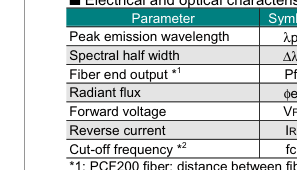
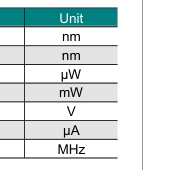
| Symbol | Condition | Min. | Typ. | Max. |
|---|---|---|---|---|
| λp | IF=30 mA | 840 | 870 | 900 |
| ∆λ | IF=30 mA | - | 45 | - |
| Pf | IF=30 mA | 30 | 45 | - |
| φe | IF=30 mA | 4.5 | 6.5 | - |
| VF | IF=30 mA | - | 1.45 | 1.6 |
| IR | VR=3 V | - | - | 10 |
| fc | IF=30 mA ± 4 mAp-p | 30 | 50 | - |

Page 2
Infrared LED L8013
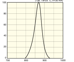
I Emission spectrum
I Frequency response
(Typ. Ta=25 ˚C, IF=30 mA ± 4 mAp-p)
(Typ. Ta=25 ˚C, IF=30 mA)
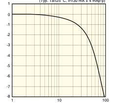
FREQUENCY (MHz)
WAVELENGTH (nm)
KLEDB0219EA
KLEDB0218EA
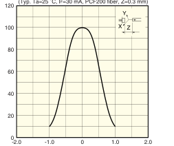
I Fiber coupling characteristics
X, Y axes
Z axis
(Typ. Ta=25 ˚C, IF=30 mA, PCF200 fiber, X, Y=0 mm)
(Typ. Ta=25 ˚C, IF=30 mA, PCF200 fiber, Z=0.3 mm)
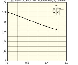
DISTANCE BETWEEN FIBER END AND CAP SURFACE Z (mm)
DISTANCE FROM CAP CENTER X, Y (mm)
KLEDB0220EA
KLEDB0221EA
I Dimensional outline (unit: mm)
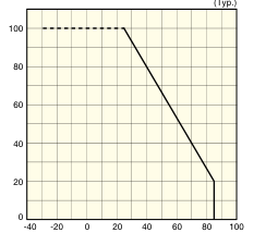
I Allowable forward current vs. ambient temperature
5.4 ± 0.2
(Typ.)
4.7 ± 0.15 WINDOW 4.0 ± 0.1
0.45 LEAD
2.54 ± 0.2
AMBIENT TEMPERATURE (˚C)
COMMON TO CASE
KLEDB0027EB
KLEDA0073EA
Information furnished by HAMAMATSU is believed to be reliable. However, no responsibility is assumed for possible inaccuracies or omissions. Specifications are subject to change without notice. No patent rights are granted to any of the circuits described herein. ©2002 Hamamatsu Photonics K.K.
HAMAMATSU PHOTONICS K.K., Solid State Division
1126-1 Ichino-cho, Hamamatsu City, 435-8558 Japan, Telephone: (81) 053-434-3311, Fax: (81) 053-434-5184, http://www.hamamatsu.com U.S.A.: Hamamatsu Corporation: 360 Foothill Road, P.O.Box 6910, Bridgewater, N.J. 08807-0910, U.S.A., Telephone: (1) 908-231-0960, Fax: (1) 908-231-1218 Germany: Hamamatsu Photonics Deutschland GmbH: Arzbergerstr. 10, D-82211 Herrsching am Ammersee, Germany, Telephone: (49) 08152-3750, Fax: (49) 08152-2658 France: Hamamatsu Photonics France S.A.R.L.: 8, Rue du Saule Trapu, Parc du Moulin de Massy, 91882 Massy Cedex, France, Telephone: 33-(1) 69 53 71 00, Fax: 33-(1) 69 53 71 10 United Kingdom: Hamamatsu Photonics UK Limited: 2 Howard Court, 10 Tewin Road, Welwyn Garden City, Hertfordshire AL7 1BW, United Kingdom, Telephone: (44) 1707-294888, Fax: (44) 1707-325777
North Europe: Hamamatsu Photonics Norden AB: Smidesvägen 12, SE-171 41 Solna, Sweden, Telephone: (46) 8-509-031-00, Fax: (46) 8-509-031-01 Italy: Hamamatsu Photonics Italia S.R.L.: Strada della Moia, 1/E, 20020 Arese, (Milano), Italy, Telephone: (39) 02-935-81-733, Fax: (39) 02-935-81-741