

 Download PDF
Multi-mode controller for SMPS
Document overview
- Manufacturer or author: STMICROELECTRONICS
- PDF pages: 51
Technical content
Datasheet sections
- 1 Description
- 2 Pin settings
- 2.1 Connections
- 2.2 Pin description
- 3 Electrical data
- 3.1 Maximum rating
- 3.2 Thermal data
- 4 Electrical characteristi cs
- 5 Application information
- 5.1 High-voltage start-up generator
- 5.2 Zero current detection and triggering block; oscillator block
- 5.3 Burst-mode operation at no load or very light load
- 5.4 Adaptive UVLO
- 5.5 PWM control block
- 5.6 PWM comparator, PWM latch and voltage feedforward blocks
- 5.7 Hiccup-mode OCP
- 5.8 Frequency modulation
- 5.9 Latched disable function
- 5.10 Soft-start and delayed latched shutdown upon overcurrent
- 5.11 OVP block
- 5.12 Brownout protection
- 5.13 Slope compensation
- 5.14 Summary of L6566B power management functions
Features
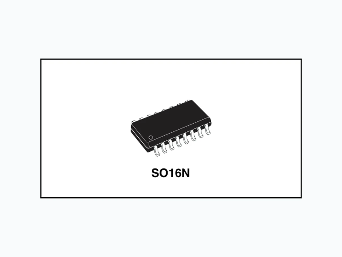
■ Selectable multi-mode operation: fixed frequency or quasi-resonant ■ On-board 700 V high-voltage start-up ■ Advanced light load management ■ Low quiescent current (< 3 mA) ■ Adaptive UVLO ■ Line feedforward for constant power capability vs mains voltage ■ Pulse-by-pulse OCP, shutdown on overload (latched or autorestart) ■ Transformer saturation detection ■ Programmable frequency modulation for EMI reduction ■ Latched or autorestart OVP ■ Brownout protection ■ -600/+800 mA totem pole gate driver with active pull-down during UVLO ■ SO16N package
Applications
■ Hi-end AC-DC adapter/charger ■ LCD TV/monitor, PDP ■ digital consumer, IT equipment ■ single-stage PFC SO16N Figure 1. Block diagram
1 Description
The L6566B is an extremely versatile current-mode primary controller ICs, specifically designed for high-performance offline flyback converters. It is also suited for single-stage single-switch input-current-shaping converters (single-stage PFC) for applications supposed to comply with EN61000-3-2 or JEITA-MITI regulations. Both fixed-frequency (FF) and quasi-resonant (QR) operation are supported. The user can pick either of the two depending on application needs. The device features an externally programmable oscillator: it defines converter’s switching frequency in FF mode and the maximum allowed switching frequency in QR mode. When FF operation is selected, the ICs work like a standard current-mode controller with a maximum duty cycle limited at 70 % min. The oscillator frequency can be modulated to mitigate EMI emissions. QR operation, when selected, occurs at heavy load and is achieved through a transformer demagnetization sensing input that triggers MOSFET’s turn-on. Under some conditions, ZVS (zero-voltage switching) can be achieved. Converter’s power capability rise with the mains voltage is compensated by line voltage feedforward. At medium and light load, as the QR operating frequency equals the oscillator frequency, a function (valley skipping) is activated to prevent further frequency rise and keep the operation as close to ZVS as possible. With either FF or QR operation, at very light load the ICs enter a controlled burst-mode operation that, along with the built-in non-dissipative high-voltage start-up circuit and the low quiescent current, helps keep low the consumption from the mains and meet energy saving recommendations. An innovative adaptive UVLO helps minimize the issues related to the fluctuations of the self-supply voltage due to transformer’s parasites. The protection functions included in this device are: not-latched input undervoltage (brownout), output OVP (auto-restart or latch-mode selectable), a first-level OCP with delayed shutdown to protect the system during overload or short circuit conditions (auto- restart or latch-mode selectable) and a second-level OCP that is invoked when the transformer saturates or the secondary diode fails short. A latched disable input allows easy implementation of OTP with an external NTC, while an internal thermal shutdown prevents IC overheating. Programmable soft-start, leading-edge blanking on the current sense input for greater noise immunity, slope compensation (in FF mode only), and a shutdown function for externally controlled burst-mode operation or remote ON/OFF control complete the equipment of this device.
Figure 2. Typical system block diagram
2 Pin settings
2.1 Connections
Figure 3. Pin connection (through top view)
2.2 Pin description
Table 1. Pin functions the UVLO threshold to allow a faster restart. this pin and kept separate from any pulsed current return. and IGBT’s with a peak current capability of 800 mA source/sink.
voltage for the signal part of the IC. action. If the function is not used, the pin will be left open. improves sensitivity to temporary disturbances. up. Ground the pin if the function is not used. voltage is pulled below 1.4 V the IC will shut down.
10 VREF
Table 1. Pin functions (continued)
11 ZCD
strobed and digitally filtered to increase noise immunity.
12 MODE/SC
maximum allowed operating frequency.
13 OSC
detecting an overload condition (OLP).
15 VFF
pulse-by-pulse current limitation (the higher the voltage, the lower the setpoint). GND (pin 3) to reduce noise pick-up.
16 AC_OK
3 Electrical data
3.1 Maximum rating
3.2 Thermal data
Table 2. Absolute maximum ratings Table 3. Thermal data
4 Electrical characteristics
unless otherwise specified). Table 4. Electrical characteristics
Table 4. Electrical characteristics (continued)
- Parameters tracking one another.
- See Table 6 on page 41 and Table 7 on page 42
- The voltage feedforward block output is given by:
5 Application information
otherwise the device will be FF-operated.
- QR mode at heavy load. Quasi-resonant ope ration lies in synchronizing MOSFET's
main benefits of this kind of operation.
- Valley-skipping mode at medium/ light load. The externally programmable oscillator of
- Burst-mode with no or very light load. When the load is extremely light or disconnected,
the converter will enter a controlled on/off operation with constant peak current. very low, no issue of audible noise arises. Figure 4. Multi-mode operation with QR option active
- FF mode from heavy to light load. The system operates exactly like a standard current
continuous to discontinuous operation mode of the transformer.
- Burst-mode with no or very light load. This kind of operation is activated in the same
way and results in the same behavior as previously described for QR operation. operation is selected) in order to mitigate EMI emissions by a spread-spectrum action.
5.1 High-voltage start-up generator
Figure 5 shows the internal schematic of the high-voltage start-up generator (HV generator). with a temperature-compensated current generator connected to its source. Figure 5. High-voltage start-up generator: internal schematic
ground and makes its voltage rise almost linearly. Figure 6. Timing diagram: normal power-up and power-down sequences to a standard start-up circuit made with external dropping resistors. protection (see the relevant section) is not used. page 20, and that the converter will work safely with extremely low power throughput.
5.2 Zero current detection and tr iggering block; oscillator block
The zero current detection (ZCD) and triggering blocks switch on the external MOSFET if a negative-going edge falling below 50 mV is applied to the input (pin 11, ZCD). To do so the triggering block must be previously armed by a positive-going edge exceeding 100 mV. This feature is typically used to detect transformer demagnetization for QR operation, where the signal for the ZCD input is obtained from the transformer’s auxiliary winding used also to supply the L6566B. The triggering block is blanked for TBLANK = 2.5 µs after MOSFET’s turn-off to prevent any negative-going edge that follows leakage inductance demagnetization from triggering the ZCD circuit erroneously. The voltage at the pin is both top and bottom limited by a double clamp, as illustrated in the internal diagram of the ZCD block of Figure 8 on page 20. The upper clamp is typically located at 5.7 V, while the lower clamp is located at -0.4 V. The interface between the pin and the auxiliary winding will be a resistor divider. Its resistance ratio will be properly chosen (see Section 5.11: OVP block on page 35) and the individual resistance values (RZ1, RZ2) will be such that the current sourced and sunk by the pin be within the rated capability of the internal clamps (± 3 mA). At converter power-up, when no signal is coming from the ZCD pin, the oscillator starts up the system. The oscillator is programmed externally by means of a resistor (RT) connected from pin OSC (13) to ground. With good approximation the oscillation frequency fosc will be: Equation 2 (with fosc in kHz and RT in kΩ). As the device is turned on, the oscillator starts immediately; at the end of the first oscillator cycle, being zero the voltage on the ZCD pin, the MOSFET will be turned on, thus starting the first switching cycle right at the beginning of the second oscillator cycle. At any switching cycle, the MOSFET is turned off as the voltage on the current sense pin (CS, 7) hits an internal reference set by the line feedforward block, and the transformer starts demagnetization. If this completes (hence a negative-going edge appears on the ZCD pin) after a time exceeding one oscillation period T osc = 1/fosc from the previous turn-on, the MOSFET will be turned on again - with some delay to ensure minimum voltage at turn-on – and the oscillator ramp will be reset. If, instead, the negative-going edge appears before Tosc has elapsed, it will be ignored and only the first negative-going edge after Tosc will turn-on the MOSFET and synchronize the oscillator. In this way one or more drain ringing cycles will be skipped (“valley-skipping mode”, Figure 9) and the switching frequency will be prevented from exceeding fosc. T osc R 102f ⋅≈
the converter or on its output voltage. cycle will take place after skipping no more than one oscillator cycle. block on page 35 for further implications of TBLANK. Figure 9. Drain ringing cycle skipping as the load is gradually reduced
ZCD the maximum pull-up current (130 μA). illustrated in the timing diagrams of Figure 10. Section 5.11: OVP block on page 35). Figure 10. Operation of ZCD, triggering and oscillator blocks (QR option active)
5.3 Burst-mode operation at no load or very light load
others previously described, is noise-free since the peak current is low. sense resistor must be determined taking this offset into account. Figure 11. Load-dependent operating modes: timing diagrams
Figure 12. Addition of an offset to the current sense lowers the burst-mode
5.4 Adaptive UVLO
generating a voltage not exceeding the maximum allowed by the control IC at full load. Figure 13. Adaptive UVLO block
5.5 PWM control block
Figure 14, left-hand side circuit). regulation, especially as a result of load changes, is quite poor. Figure 14. Possible feedback configurations that can be used with the L6566B voltage tolerance is in the range of ± 10 %.
5 Vcc
Figure 15. Externally controlled burst-mode operation by driving pin COMP: timing
5.6 PWM comparator, PWM latch and voltage feedforward blocks
might result from the noise generated (“double-pulse suppression”). csx, thereby, determines the overcurrent setpoint along with the sense resistor Rs. function available to solve this issue.
no more than a couple of iterations. biased at a fixed voltage using a divider from VREF (pin 10). Figure 17. Left: overcurrent setpoint vs VFF voltage; right: line feedforward function block
a clean operation of the IC even in a noisy environment.
5.7 Hiccup-mode OCP
Figure 18. Hiccup-mode OCP: timing diagram
5.8 Frequency modulation
Figure 19. Frequency modulation circuit triangle will be little affected.
0.5 V0 V
Application information L6566B Equation 9 which is the parameter that the amplitude of the generated side-band harmonics depends on. The minimum frequency fsw_min (occurring on the peak of the triangle) and the maximum frequency fsw_max (occurring on the valley of the triangle) will be symmetrically placed around the centre value fsw, so that: Equation 10 Then, RT will be found from (5) (see Section 5.2: Zero current detection and triggering block; oscillator block on page 21), while RMOD and CMOD can be calculated as follows: Equation 11 where Δfsw and fm (in kHz, with CMOD in nF and RMOD in kΩ) will be selected by the user so to achieve the best compromise between attenuation of peak EMI emissions and clean converter operation.
5.9 Latched disable function
The device is equipped with a comparator having the non-inverting input externally available at the pin DIS (8) and with the inverting input internally referenced to 4.5 V. As the voltage on the pin exceeds the internal threshold, the device is immediately shut down and its consumption reduced to a low value. The information is latched and it is necessary to let the voltage on the Vcc pin go below the UVLO threshold to reset the latch and restart the device. To keep the latch supplied as long as the converter is connected to the input source, the HV generator is activated periodically so that Vcc oscillates between the start-up threshold V ccON and VccON - 0.5 V. Activating the HV generator in this way cuts its power dissipation approximately by three (as compared to the case of continuous conduction) and keeps peak silicon temperature close to the average value. To let the L6566B restart it is then necessary to disconnect the converter from the input source. Pulling pin 16 (AC_OK) below the disable threshold (see Section 5.12: Brownout protection on page 37) will stop the HV generator until Vcc falls below Vccrestart, so that the latch can be cleared and a quicker restart is allowed as the input source is removed. This operation is shown in the timing diagram of Figure 20 on page 33. m sw f fΔ=β sw2 swmax_swsw2 swmin_sw fff;fff Δ+=Δ−= sw MOD f 102R Δ m MOD f 75C =
(e.g. 1-10 nF) to prevent any malfunctioning of this kind. Figure 20. Operation after latched disable activation: timing diagram
5.10 Soft-start and delayed latc hed shutdown upon overcurrent
5.11 OVP block
T a b l e7 o n p a g e4 5) for additional hints. Figure 22. OVP function: internal block diagram number of the secondary winding and Naux the turn number of the auxiliary winding.
where TBLANK2 = 2 µs; this is also illustrated in the diagram of Figure 24.
5.12 Brownout protection
mains voltage falls below the minimum specification of normal operation. down, hence causing the output voltage not to decay to zero monotonically. quicker restart as the input source is removed. HV generator restart thresholds, as shown in the timing diagram of Figure 25. Figure 24. Maximum allowed duty cycle vs switching frequency for correct OVP
Figure 26. Voltage sensing techniques to implement brownout protection with the the unit to restart, which may take even several seconds. circuit is suitable to have a quick restart after a latched shutdown. to ground with a small film capacitor (e.g. 1-10 nF) to prevent any malfunctioning of this kind. the pin has to be connected to Vcc through a resistor (220 to 680 kΩ).
5.13 Slope compensation
continuous conduction mode with a duty cycle close to or exceeding 50 %. Figure 27. Slope compensation waveforms programming resistor is needed to ensure a clean operation at light loads. If slope compensation is not required with FF operation, the pin shall be left floating.
5.14 Summary of L6566B power management functions
Table 5. L6566B light load management features
Table 6. L6566B protections
- Use One external diode from V FF (#15) to AC_OK (#16), cathode to AC_OK
- Use one external diode from SS (#14) to V REF (#10), cathode to VREF
- If C ss and the Vcc capacitor are such that Vcc falls below UVLO before latch tripping (Figure 21 on page 34)
- If C ss and the Vcc capacitor are such that the latch is tripped before Vcc falls below UVLO (Figure 21 on page 34)
- Discharged to zero by V cc going below UVLO
Table 6. L6566B protections (continued)
6 Application examples and ideas
Figure 28. Typical low-cost application schematic
264 Vac
Figure 29. Typical full-feature appl ication schematic (QR operation)
Figure 30. Typical full-feature application schematic (FF operation) Table 7. External circuits that determine IC behavior upon OVP and OCP
Figure 31. Frequency foldback at light load (FF operation) Figure 32. Latched shutdown upon mains overvoltage
15 L6566B8 VFF
7 Package mechanical data
In order to meet environmental requirements, ST offers these devices in ECOPACK® packages. These packages have a lead-free second level interconnect. The category of second Level Interconnect is marked on the package and on the inner box label, in compliance with JEDEC Standard JESD97. The maximum ratings related to soldering conditions are also marked on the inner box label. ECOPACK is an ST trademark. ECOPACK specifications are available at: www.st.com.
Figure 33. Package dimensions Table 8. SO16N mechanical data
8 Order codes
Table 9. Order codes
9 Revision history
Table 10. Document revision history