

 Download PDF
L6364 STMICROELECTRONICS
Document overview
- PDF pages: 60
Technical content
Page 1
Datasheet
Dual channel transceiver IC for SIO and IO-Link sensor applications
Features
Supply voltage from 5 V to 35 V 2.5 V to 5 V compatible I/Os 3.3 V and 5 V, 50 mA linear regulators 50 mA DC-DC regulator with configurable frequency (0.5 MHz to 2 MHz) & voltage (5 V to 10.5 V) Low dissipative (5 Ω) CQ and DIO output stages configurable in high side, low side, push/pull Configurable reporting threshold (0.11 A to 0.25 A) of current limitation for CQ and DIO lines Configurable reporting threshold (0.22 A to 0.5 A) of current limitation for CQ//DIO line (Join Mode) Fully protected: – Embedded reverse polarisation diode (DOUT pin) – Full zero current reverse polarity between VPLUS, CQ, DIO and PGND pins – Configurable (up to 216°C) thermal shutdown threshold
– 7-bit, calibrated, temperature measurement – Configurable (6.0 V to 15 V) VPLUS undervoltage detection – CQ and DIO short-circuit current limit and reporting
- -40 to +150°C operating temperature
- Suitable to drive L, C and R loads
- Quartz-free IO-Link clock extraction and timing generation at COM2 (38.4k
Product status link
Baud) and COM3 (230.4k Baud)
- Integrated UART peripheral with M-sequence handling (inc. checksum) for all IO-Link sequences according to specification v1.1
| Product summary | ||
| Order code | L6364Q | L6364W |
| Package | QFN 20L | CSP 19 |
| Packing | Tape & Reel | Tape & Reel |
- Multi octet UART mode for M-sequence size up to 15 octets
- Single octet UART mode for unlimited M-sequence size and continuous data transfer
- Transparent UART mode for special applications CQ and DIO switching time = 100 ns (2 kΩ//2.2 nF load)

8 V Zener limits for fast demagnetization of inductive loads Two LED drivers with configurable (up to 8 mA) current Design to meet application requirements: – ESD IEC 61000-4-2 protection to 4 kV – EMC protection against surge (500 Ω coupling) above ±2A/50 μs
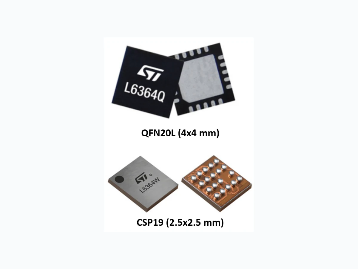
- Smart format QFN-20L 4x4 mm and CSP-19 2.5x2.5 mm packages
Application
- Industrial sensors
- Factory automation
- Process control
DS13363 - Rev 4 - October 2021
www.st.com
For further information contact your local STMicroelectronics sales office.
Page 2
Description
1
Description
The L6364 is a dual channel transceiver for industrial sensor applications. It has been designed to support even the IO-Link standard and acts as a bridge between a microcontroller with a sensor or actuator function and a 24 V supply and signaling cable. In normal operation the L6364 is configured at start up by the microcontroller via the SPI interface. Typically, the L6364 then operates as a Single Input Output device driving the output lines as configured by the microcontroller. If the device is connected to an IO-Link master, then the master can initiate communication and exchange data with the microcontroller while the L6364 acts as a physical layer for the communication.
The L6364 integrates a surge pulse suppressor circuit featuring the protection of the process side pins (VPLUS, CQ, DIO, PGND) against up to ±1.5 kV/50 us withstand pulses applied with 500 Ω coupling. Also, the same pins are protected against reverse polarity (Section 20 Surge pulse and reverse polarity protections). The two symmetrical input/output stages (CQ and DIO) can be used either for the communication through the 24 V data bus or to drive industrial loads. Each output stage can be configured (Hi-Z, High Side, Low Side, Push-Pull) and protected against overload by the ISET programmable threshold (110 mA to 250 mA). Also, the JOIN mode configuration allows to reduce power dissipation and to double overload threshold by shorting CQ and
DIO on the application. The IC embeds two linear regulators (V3V3 and V5V) than can work either directly supplied by the external supply rail (VPLUS) or by the high efficiency and configurable (VSET, fSET) embedded DC-DC converter. The output voltage of the DC-DC can be used as additional supply rail for the application. The total current capability (IOUT) of the internal regulators and DC-DC is 50 mA. The logic core of the IC is internally supplied by the V3V3 rail and communicates with the external microcontroller by an SPI (slave) interface, an interrupt signal (INT) and direct driving of DIO line (CTLD). The VDIG pin defines the voltage rail of these digital signals: it enables the IC to work even with microcontroller supplied by different
rails than V3V3. The internal logic embeds an IO-Link UART peripheral that can be configured by the microcontroller in one of the three possible options: Transparent, Single-octet or Multi-octet (Section 8 IO-Link UART peripheral). In Transparent mode the IC works purely as a physical layer between the microcontroller and the 24 V data bus: the workload for the management of the input/output data is fully demanded to the firmware running on the microcontroller. In Single-octet and Multi-octet modes the IC itself does a set of IO-Link required checks on the input/output data with consequent drastic reduction of the workload for the microcontroller. The Multi-octet is
usually preferred when the data transfer with the IO-Link master can be managed by the available 8-bits registers buffer: the IC generates an interrupt to microcontroller when all data in the buffer are ready. If IO-Link data transfer exceeds the IC buffer capability, then Single-octet can be used instead: in this case the IC generates an interrupt at every octet ready. The L6364 offers two programmable pins (LED1 and LED2) acting as LED drivers with configurable current capability (up to 8 mA, each).
page 2/60
Page 3
Block Diagram
2
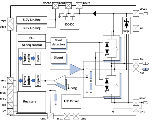
Block Diagram
Figure 1. Block Diagram
page 3/60
Page 4
Package and pin-out
3
Package and pin-out
Figure 2. Package and pin-out - QFN
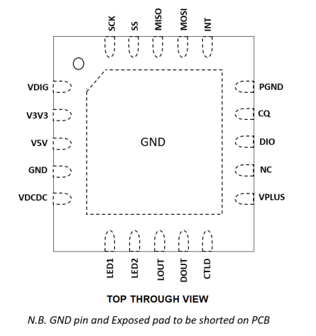
Figure 3. Package and pin-out - CSP
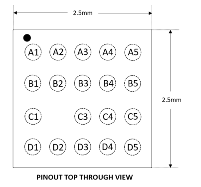
page 4/60
Page 5
Package and pin-out
Table 1. Pin Description
| Group/Exposure | Pin number (QFN) | Pin number (CSP) | Name | Function | Type (1) |
|---|---|---|---|---|---|
| Line (Process side)/ External | 11 | D1 | VPLUS | Line supply voltage | PWR |
| 14 | B1 | CQ | Line data signal SIO/SDCI | ANA IO | |
| 13 | C1 | DIO | Line data signal DI/DO | ANA IO | |
| 15 | A1 | PGND | Switch ground return | PWR | |
| 4, TAB | C5 | GND | Ground | PWR | |
| SPI, INT, CTLD (Logic side)/Internal | 17 | A3 | MOSI | SPI data, microcontroller to L6364 | CI |
| 19 | A4 | SS | SPI synchronization, slave select | CI | |
| 20 | B4 | SCK | SPI interface clock signal | CI | |
| 18 | B3 | MISO | SPI data, L6364 to microcontroller | COZ | |
| 16 | A2 | INT | Interrupt | CO | |
| 1 | A5 | VDIG | Supply to IC internal IO level shifting logic: usually connected to the same supply rail of the microcontroller. (2) | PWR | |
| 10 | B2 | CTLD | Direct control of DIO output channel | CI | |
| LED/External | 6 | C3 | LED1 | LED1 source current | ANA O |
| 7 | D5 | LED2 | LED2 source current | ANA O | |
| Low voltage supply/ Internal | 3 | C4 | V5V | Sensor and microcontroller supply | PWR |
| 2 | B5 | V3V3 | PWR | ||
| DC-DC/Internal | 9 | D2 | DOUT | VPLUS following diode protections | ANA IO |
| 8 | D3 | LOUT | Inductor power feed | ANA IO | |
| 5 | D4 | VDCDC | DC-DC supply output, intermediate supply | PWR | |
| Unused/Internal | 12 | C2 | N/C | Not connected | - |
- PWR: power, CI: CMOS input, CO: CMOS output, COZ: output with tristate function, ANA IO: Analogue input output, ANA O: Analogue output. 2. although the internal core of the IC is supplied by the V3V3, the full operation is guaranteed even when VDIG is connected either to 2.5 V, 3.3 V, 5.0 V or 5.5V rail.
page 5/60
Page 6
Technical Data
4
Technical Data
4.1
Absolute Maximum Ratings
Absolute maximum ratings are those values beyond which damage to the device may occur. Functional operation under these conditions is not implied. All voltages are referenced to GND unless otherwise specified.
Table 2. Absolute maximum ratings
| Symbol | Parameter | Value | Unit |
|---|---|---|---|
| VVPLUS, VCQ, VDIO | Pin Voltage (steady-state) | - 35 to + 35 | V |
| Pin Voltage (during surge pulse transient with 500 Ω coupling, ISURGE < ± 3 APK) | - 45 to + 45 | ||
| VV5V | 5V voltage pin | - 1 to 7 | V |
| VV3V3 | 3.3V voltage pin | - 1 to 5 | V |
| VDIG, VLED1, VLED2 | Digital pins (SPI, CTLD, INT, VDIG) and LED pins | - 1 to 7 | V |
| VESD | Electrostatic protection (HBM) | 2 | kV |
| PD | Power Dissipation | Internally limited | W |
| TLEAD | Soldering temp. (20-40sec, cf. JEDEC J-STD-020C) | 260 | °C |
| TSTOR | Storage Temperature Range | -40 to 150 | °C |
Operation above the absolute maximum ratings may lead to instantaneous device failure. Operation of the L6364 between the operating ratings and the absolute maximum ratings leads to a reduced operating lifetime.
4.2
Thermal Characteristics
Table 3. Thermal data
| Symbol | Parameter | Value | Unit | |
|---|---|---|---|---|
| QFN20L | CSP19 | |||
| Rth(JA) | Thermal resistance junction-ambient on evaluation boards(1) | 54 | 80 | °C/W |
| Thermal resistance junction-ambient as per JEDEC specification (JESD51-7) (2) | 38 | 43.4 | ||
- 2s, FR4, Cu thickness = 35 μm 2. 2s2p, FR4 under still air conditions
4.3
Recommended operating conditioning
Table 4. Recommended operating conditions
| Symbol | Parameter | Min. | Typ. | Max. | Unit |
|---|---|---|---|---|---|
| IQUIES | Operating current supply, no pin currents, DC-DC enables | 3.0 | 3.5 | mA | |
| IQUIES_START | Operating current supply on pin VPLUS during startup | 10 | mA | ||
| VSUP | VPLUS supply voltage, IV3v3= 50 mA, (DC-DC disabled) | 4.5 | 24 | 35 | V |
page 6/60
Page 7
Electrical Characteristics
| Symbol | Parameter | Min. | Typ. | Max. | Unit |
|---|---|---|---|---|---|
| VSUP | VPLUS supply voltage, IV5V0= 50 mA, (DC-DC disabled) | 6 | 24 | 35 | V |
| Minimum VPLUS (DC-DC enabled) (see Figure 15) | 10.5 | V | |||
| VDCDC_5V_MIN | Minimum VDCDC output voltage (VSET) for use of V5V | 6.1 | V | ||
| CBLK | Blocking capacitor on VPLUS | 100 | nF | ||
| CEMC | EMC blocking capacitor | 470 | pF | ||
| CV3V3 | Capacitor CV3V3 | 1 | 10 | μF | |
| CV5V | Capacitor CV5V (V5V in use) | 1 | 10 | μF | |
| CDOUT | Capacitor CDOUT | 0.01 | 1 | μF | |
| CDCDC | Capacitor CDCDC | 2.2 | uF | ||
| LDCDC | Inductor LDCDC | 220 | uH | ||
| CQLOAD_MAX | Maximum load capacitor CQ (see Figure 21)(1) | 250 | nF | ||
| CDIOLOAD_MAX | Maximum load capacitor DIO (see Figure 21) (1) | 250 | nF | ||
| CJOINLOAD_MAX | Maximum load capacitor JOIN mode (see Figure 22) (1) | 500 | nF | ||
| LCQLOAD_MAX | Maximum load inductance CQ (see Figure 21) | (2) | mH | ||
| LDIOLOAD_MAX | Maximum load inductance DIO (see Figure 21) | (2) | mH | ||
| LJOINLOAD_MAX | Maximum load inductance JOIN mode (see Figure 22) | (2) | mH |
- values measured with pure capacitive load. 2. unlimited, see Section 19 for further details.
4.4
Electrical Characteristics
Electrical parameters are valid over the operating temperature and voltage range, unless otherwise stated.
Table 5. Receiver CQ/DIO
| Symbol | Parameter | Test Conditions | Min. | Typ. | Max. | Unit |
|---|---|---|---|---|---|---|
| VTHH | Input threshold “H” | RF bit = 0 in CFG register (see Table 32. Register map ). | 10.5 | 13 | V | |
| VTHL | Input threshold “L” | 8 | 11.5 | V | ||
| VTHHR | Input threshold “H” | RF bit = 1 in CFG register (see Table 32. Register map ). | -10% | (VVPLUS/1.8)-0.5 | +10% | V |
| VTHLR | Input threshold “L” | -10% | (VVPLUS/1.8)+0.5 | +10% | V | |
| VHYS | Hysteresis | 0.5 | 1 | 1.5 | V | |
| VIN | Input range CQ/DIO | 35 VVPLUS +10 | V | |||
| fBIT | Data rate | BD bit = 0 in CFG register (see Table 32. Register map ). | 38.4 | kBaud | ||
| BD bit = 1 in CFG register (see Table 32. Register map ). | 230.4 | kBaud | ||||
| TBIT | Bit time | 1/fBIT | μs |
page 7/60
Page 8
Electrical Characteristics
| Symbol | Parameter | Test Conditions | Min. | Typ. | Max. | Unit |
|---|---|---|---|---|---|---|
| fCK | Internal clock base | -10% | 10 | +10% | MHz |
Table 6. Short-circuit and Wake-up detection
| Symbol | Parameter | Test Conditions | Min. | Typ. | Max. | Unit |
|---|---|---|---|---|---|---|
| ISHORT | Set current tolerance | See Table 28 | -20% | ISET | +20% | mA |
| tSHORT | Filter delay | -10% | 14 | +10% | μs | |
| NSHORT | Number of activation attempts/retry | SIO bit = 1 in CCTL register (see Table 32. Register map ). | 2 | |||
| tRETRY | Retry delay | -10% | 50 | +10% | μs | |
| tRESTART | Short-circuit restart time | -10% | 100 | +10% | ms |
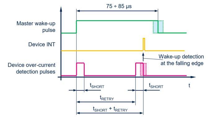
Figure 4. Example of Wake-up sequence timing (VCQ = green plot; ICQ = red plot; VINT = Yellow)
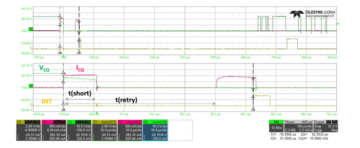
Table 7. POR (Power On Reset)
| Symbol | Parameter | Test Conditions | Min. | Typ. | Max. | Unit |
|---|---|---|---|---|---|---|
| VPOR | POR release threshold | 1.6 | 2 | 2.5 | V | |
| VHYST | POR hysteresis | 0.1 | V |
Table 8. Output switches individual channels CQ/DIO
| Symbol | Parameter | Test Conditions | Min. | Typ. | Max. | Unit |
|---|---|---|---|---|---|---|
| RSW | Output resistance | IOUT = 100mA | 5 | 10 | Ω | |
| VZEN | Zener voltage | IOUT = 10mA | 6 | 10 | V | |
| IOUT = 100mA | 8 | V | ||||
| ISAT | Saturated current | 1.2 | A |
page 8/60
Page 9
Electrical Characteristics
Table 9. Line surge protection, parameters with respect to any pair PGND, CQ, DIO, VPLUS
| Symbol | Parameter | Test Condition | Min. | Typ. | Max. | Unit |
|---|---|---|---|---|---|---|
| VSURGE(LEAKAGE ) | Internal Surge clamps leakage | V = ±35 V | 10 | 40 | μA | |
| VSURGE(THRESHO LD) | Internal Surge clamps activation threshold | I = ±100mA | ±35 | ±40 | ±45 | V |
Table 10. Thermal shutdown
| Symbol | Parameter | Test Condition | Min. | Typ. | Max. | Unit |
|---|---|---|---|---|---|---|
| εT | Temperature accuracy | 150°C | -10 | 10 | °C | |
| εT | Temperature accuracy | 30°C | -5 | 5 | °C | |
| ΘHYST | Thermal hysteresis | 10 | °C |
Table 11. Digital pins
| Symbol | Parameter | Test Condition | Min. | Typ. | Max. | Unit |
|---|---|---|---|---|---|---|
| VDIG | Voltage drop on digital pins | IDIG = -4 mA | 0.5 | V | ||
| VDL | Input low signal | 0.15 VDIG | V | |||
| VDH | Input high signal | 0.5 VDIG | V | |||
| tcl | Clock low phase | SCK | 50 | ns | ||
| tch | Clock high phase | SCK | 50 | ns | ||
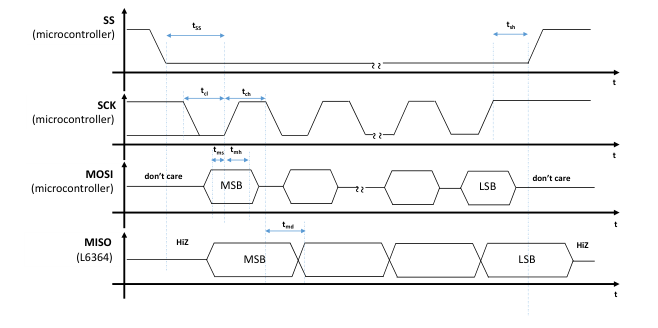
| tms | Setup wrt. SCK | MOSI | 10 | ns | ||
| tmh | Hold wrt. SCK | MOSI | 10 | ns | ||
| tss | Setup wrt. SCK | SS | 10 | ns | ||
| tsh | Hold wrt. SCK | SS | 10 | ns | ||
| tmd | Output availability | MISO | 18 | 40 | ns | |
| RPU | Pull-up resistance | SS, SCK, MOSI | 50 | 200 | kΩ | |
| RPD | Pull-down resistance | CTLD | 50 | 200 | kΩ |
Table 12. LED Driver
| Symbol | Parameter | Test Condition | Min. | Typ. | Max. | Unit |
|---|---|---|---|---|---|---|
| ILED | Sink current base unit(1) | See Figure 13 | -10% | 0.5 | +10% | mA |
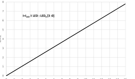
- The current supplied by each LED pin can be configured between 0 to 8 mA by LED1[3:0] and LED2[3:0] of LED register (address 0x07). One bit increment of LEDx[3:0] corresponds to +0.5 mA(typ).
Table 13. Linear regulators
| Symbol | Parameter | Test Condition | Min. | Typ. | Max. | Unit |
|---|---|---|---|---|---|---|
| IPLUSREV | Power fail reverse leak | VDCDC = DOUT = 35 V VPLUS = GND | 10 | μA | ||
| IOUT | Regulator output capability | Load on V3V3 or V5V pin | 50 | mA | ||
| RSTART_MIN | Startup static capability | 67 | Ω |
page 9/60
Page 10
Electrical Characteristics
| Symbol | Parameter | Test Condition | Min. | Typ. | Max. | Unit |
|---|---|---|---|---|---|---|
| VV3V3 | Regulator output voltage | 0 mA < IV3V3 <50 mA | 3.0 | 3.3 | 3.6 | V |
| VV5V | Regulator output voltage | 0 mA < IV5V < 50 mA | 4.5 | 5.0 | 5.5 | V |
| IPD5V | Pull-down current of V5V pin | 50 | 100 | 200 | μA | |
| VUV | Undervoltage detect | see Table 29, VUV < 10 V | UVSET-1 | UVSET | UVSET+1 | V |
| VUV ≥ 10 V | UVSET-10% | UVSET | UVSET+10% | V |
Table 14. DC-DC supply
| Symbol | Parameter | Test Condition | Min. | Typ. | Max. | Unit |
|---|---|---|---|---|---|---|
| VVPLUS | Supply voltage | VVPLUS > target Output voltage of DC-DC (see Table 31. DC-DC output voltage, VSET) | 35 | V | ||
| VDIODE | Voltage drop on internal diode between VPLUS and DOUT pins | IDIODE = 20 mA | 850 | mV | ||
| IOUT | DC-DC Output current | 50 | mA | |||
| |VSET_TOL| | VSET tolerance | see Table 31. DC-DC output voltage, VSET | -10% | VSET_NOM | +10% | V |
| tVSET | VSET step size | 52 | µs | |||
| ∆tVSET | VSET range delay | VSET_MIN ⇄ VSET_MAX | 7*tVSET_MIN | 7*tVSET_MAX | µs | |
| RDCDC | Output voltage load regulation | 0 - 50 mA | 2 | Ω | ||
| ISTARTUP | Startup current | From pin VPLUS, See Section 17.3.1 | 50 | 80 | 140 | mA |
| VSTARTUP | Startup voltage | On pin VDCDC, See Section 17.3.1 | 7.5 | 8.0 | 8.5 | V |
| VVPLUSDCMIN | DC-DC operation start | 7.0 | 8.0 | 9.0 | V | |
| VDCMIN | Minimum internal core voltage to enable DC-DC | 2.8 | V | |||
| fDCDC | Operating frequency | see Table 30 | -10% | fSET | +10% | kHz |
| RHIGH | High side resistance | 3.3 | 6.6 | 20 | Ω | |
| RLOW | Low side resistance | 4.5 | 7.2 | 20 | Ω | |
| ILIMIT | ILIMIT in inductor | 70 | 90 | mA | ||
| RSHUNT | Sense resistance | 0.6 | 1 | 1.5 | Ω |
page 10/60
Page 11
Startup
5
Startup
At startup, power is applied via the cable on VPLUS. The embedded Power-On-Reset (POR) circuit ensures the proper startup of the L6364 with the output switches initially in a high impedance state. The device core of the L6364, including the control for the 5 V regulator, is supplied by the V3V3 supply.
The SPI communication logic is reset whenever SS='1' and is independent of the L6364 power on reset itself. It is therefore possible to read the SPI register values even when the L6364 is in reset. In particular, the STATUS:RST bit is read as part of the STATUS byte on every SPI access.
This bit is cleared when the device is in reset, or when the device has been reset. This status information can be used as set out in Table 15 to determine the L6364 reset state, and also to react to unexpected reset conditions.
Table 15. L6364 Reset conditions
| Device state | STATUS:RST | INT | Comment |
| Power-On-Reset (POR) | 0 | 0 | L6364 is in power on reset (checked at the start of the SPI access). Only the STATUS:RST bit is valid. The microcontroller may wait for a high level on INT before proceeding. |
| Device reset (post POR) | 0 | 1 | L6364 has been reset, and the INT line is forced high. Write STATUS:RST='1' to allow normal operation of the L6364. |
| Operation | 1 | X | Normal operation |
The microcontroller should initialize the state of the internal registers to the desired values after reset.
page 11/60
Page 12
SPI Communication
6
SPI Communication
Internal registers (see Table 32. Register map) are provided to observe and control the L6364 state. These register settings are read and written via the SPI interface, where the L6364 is the SPI slave. The operating voltage level for inputs and outputs on the SPI interface is set by the VDIG pin. Usually, this pin is directly connected either to the V5V or V3V3 pins (Section 23 Typical Applications). However, full functionality of the IC is guaranteed even when VDIG pin is connected to 2.5 V, or 3.3 V, or 5.0 V or 5.5 V rail, although the internal core works at the V3V3 rail.
The detailed timing diagram is shown in Figure 5 Data is shifted into an internal shift register from input MOSI on each rising SCK edge. Data is made available on pin MISO at each falling SCK edge. Note that the MISO line is only driven when the slave specific select line is SS='0', which allows other SPI slaves to share the same SPI bus.
The MSB of the address byte is a WR/RDn bit, where a '1' indicates that each byte is written to the registers. Valid data is always made available on the MISO line independent of the WR/RDn bit.
Where a register is written and read in the same operation, then the read value is the old register value. During read operations, the level of the MOSI line is ignored for the data bytes.
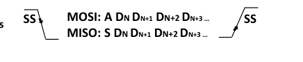
The byte sequence for data transmission is shown in Figure 6. Each transmission sequence consists of a falling SS edge which synchronizes transmission, followed by a target register address byte.
During the transmission of the address byte from the microcontroller to the L6364, the status register contents are sent from the L6364 to the microcontroller.
Figure 5. Register programming.
6.1
Multiple byte exchange
Multiple registers at consecutive addresses can be read or written by extending the access as shown in Figure 6; bytes are written on the rising SCK clock edge of the eighth bit of each byte.
With the WR/RDn bit set, a simultaneous read/write operation is started. Now, with a multiple byte exchange, it is possible to both read and write the values of multiple register bytes in one operation. This is particularly useful with larger M-sequence types where there is limited time available for the SPI exchange.
page 12/60
Page 13
Multiple byte exchange
Figure 6. Single byte and sequential byte accesses
Consecutive access

SS
Single access
KEY: A: Address byte, D: Data byte, S: Status byte
page 13/60
Page 14
DIO pin
7
DIO pin
The DIO pin is a fully protected I/O which is driven or sampled independently via SPI. This pin may be operated in one of two modes:
- JOIN mode (DCTL:DIO bit = '0'). This is the default configuration for DCTL:DIO bit. The DIO/CQ outputs function together to provide a single, double drive strength, IO-Link conformal output. The outputs, DIO and CQ, must be externally shorted together. When in this mode, the DCTL:HS and DCTL:LS no longer have any effect on the output state.
- DIO mode (DCTL:DIO bit = '1'). The DIO line functions as independent high voltage digital input output pin. Setting bit DCTL:IEN in this mode, enables a signal level change interrupt, informing the microcontroller that a level change has occurred on the DIO line.
7.1
DIO mode output control
In DIO mode there are two alternatives for controlling the pin output state: via SPI (DCTL:EXT reset) or directly via pin CTLD (DCTL:EXT set). Table 16 and Table 17 show how the output is controlled in both cases respectively.
Table 16. DIO control via SPI-DCTL:EXT=’0’
| Mode | DCTL:HS | DCTL:LS | DIO Channel Output State |
| Off | 0 | 0 | HiZ |
| Low | 0 | 1 | 0 |
| High | 1 | 0 | 1 |
| Illegal | 1 | 1 | HiZ |
If bit DCTL:EXT is set, bits DCTL:HS and DCTL:LS function as configuration bits, which configure the DIO output to be a PNP, NPN or Push-Pull driver.
Table 17. Direct DIO control via pin CTLD – DCTL:EXT=’1’
| DIO Channel Output State | ||||
| Mode | DCTL:HS | DCTL:LS | CTLD=’1’ | CTLD=’0’ |
| Inactive | 0 | 0 | HiZ | HiZ |
| NPN | 0 | 1 | 0 | HiZ |
| PNP | 1 | 0 | 1 | HiZ |
| Push-Pull | 1 | 1 | 1 | 0 |
The high- and low-side switches are identical and have an on-state resistance of RSW. Any inactive switch acts as a Zener diode limiting the voltage on the DIO line to VZEN above VVPLUS (high-side switch), or VZEN below GND (low-side switch). This allows rapid switch-off for inductive loads.
The DIO data level is monitored for signals, filtering out pulses with a duration of less than (1/16) \* TBIT, see Table 5. The decision threshold for the DIO data level is determined by the CFG:RF bit. Where this is '0', the IO-link standard absolute levels are used, and where the bit is '1' the threshold is referred to VVPLUS/1.8.
page 14/60
Page 15
SIO mode control
7.2
SIO mode control
In the SIOActive state, the high-side or low-side switches are switched according to the CCTL:HS and CCTL:LS bits. It is not legal to switch on both simultaneously, and this register setting disables both switches.
The high-side and low-side switches are identical, and have an on-state resistance of RSW. Any inactive switch acts as a Zener diode limiting the voltage on the CQ line to VZEN above VPLUS (high-side switch), or VZEN below GND (low-side switch). This allows rapid switch-off for inductive loads.
page 15/60
Page 16
IO-Link UART peripheral
8
IO-Link UART peripheral
The L6364 contains an IO-Link UART peripheral for bidirectional communication according to the IO-Link Standard. The peripheral is controlled, and data is exchanged, via SPI register accesses. In an application where pins CQ and DIO are coupled together i.e. JOIN mode, then a reference to CQ in the following refers to the shorted pair.
Multi-octet UART mode
8.1
8.1.1
SIO Mode Figure 7 shows the IO-Link UART peripheral state machine. When the CCTL:SIO bit is set, the L6364 is set to Single Input Output mode. In this mode the L6364 has the following states:
- SIOActive: The CQ line is driven according to the setting of the HS and LS bits of CCTL register. The internal UART does not run in this state and so master messages are only detected if a wake-up request from the master is received, which switches the L6364 to the SIOListen state. If the output is set to high impedance (CCTL:HS=LS='0'), then the L6364 can not receive a wake-up request from the master. It is therefore necessary to switch to IO-Link mode (CCTL:SIO='0') if communication detection is required with a high impedance output.
- SIOListen: The L6364 has experienced a short-circuit via a wake-up request from the master. Both high-side and low-side switches are off, and the restart timer is running. Transitions on the CQ line are read as data, and stored in the data buffer (FR0 to FR14 registers). If a complete, valid, master message is received, then the state changes to Transmit, an interrupt is generated and the restart timer is reset. If the timer expires, then the L6364 returns to the SIOActive state and the CQ line is driven again after the transmission.
8.1.2
IO-Link mode At startup, and if the SIO bit is cleared, the L6364 enters IO-Link mode. In this mode the L6364 has the following states:
- IOListen: Transitions on the CQ line are read as data, and stored in the data buffers. Once a complete master message has been read, or an error is experienced in reception (e.g. bad parity, checksum or time-out), then the state changes to Transmit.
8.1.3
Transmit mode Following reception of an IO-Link master message the L6364 enters the following state:
- Transmit: The L6364 is waiting on data from the microcontroller, or is in the process of transmitting data on the CQ channel. The L6364 reverts to IOListen or SIOActive on completion of the transmission, or if an abort is generated by the microcontroller by setting END bit in the LINK register. If the L6364 has entered Transmit from an SIO mode, the microcontroller would normally now set the L6364 to IO-Link mode, such that the L6364 continues to listen for further information from the master. If the L6364 experiences a short-circuit during Transmit, then the STATUS:SSC bit is set, and the L6364 returns to either IOListen or SIOListen.
page 16/60
Page 17
Multi-octet UART mode
8.1.4
IO-Link UART peripheral (Multi-octet mode) state machine
Figure 7. IO-Link UART peripheral state machine
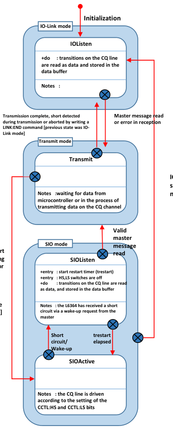
IO-LINK mode set by the microcontroller
Transmission complete, short detected during transmission or aborted by writing a LINK:END command [previous state was SIO mode]
8.1.5
Interrupt handling
The L6364 signals an event to the microcontroller using the INT pin, which is intended to be configured as a level sensitive interrupt.
page 17/60
Page 18
Multi-octet UART mode
8.1.6
Data interrupt handling If the STATUS:DAT bit is read as active (high) on an SPI access, then the L6364 is halted in a WAIT condition and is waiting for either a LINK:END or LINK:SND command from the microcontroller. While the L6364 is in the WAIT condition the interrupt pin (INT), the STATUS:INT bit and the STATUS:DAT bit remain active continuously. Data can be read and written to the L6364 registers while in the WAIT condition. Typically the LINK register and FR registers are accessed to read the incoming data, and the FR registers are written to set up the outgoing data. As the L6364 is halted, it doesn't generate further data interrupts in the WAIT
condition. When the microcontroller sends either a LINK:END or LINK:SND command, the interrupt pin (INT), the STATUS:INT bit and the data bit, STATUS:DAT, are cleared within 220 ns of the last SCK edge of the SPI write access. If the microcontroller detects an active interrupt after the SPI access, or if the STATUS:DAT bit is read as active (high) on a subsequent SPI access, then new data is available. The LINK register is duplicated as LINK2 at address 0xF to optimize sequential SPI access:
- a sequential SPI read can be used to read the LINK2 register and then the frame registers in one SPI operation.
- a sequential SPI write (including SND bit) can be used to write the LINK2 register and then the frame registers. Transmission starts once the FR0 register is written and the micro-controller must ensure that the subsequent registers have valid values before the start of transmission of the respective octets.
Short-circuit, overtemperature and undervoltage interrupt handling
8.1.7
The INT pin and the STATUS:INT bit are additionally active (high) if the last value of the short-circuit, undervoltage or overtemperature status bits communicated on the SPI is different to the current value. The L6364 handles short-circuit and overtemperature autonomously and does not require a reaction from the microcontroller.
It is possible for these status bits to change at any time, and so the interrupt may be removed between entering the interrupt service routine and reading the status on the SPI.
The interrupt is removed during the next SPI access to the L6364. If an SPI access is made without checking the value of these bits, as is typical during processing of a data interrupt, it is normal to record the status values from the final access, or to explicitly add an extra SPI access.
8.1.8
Interrupt handler structure The interrupt handler will typically have the following sequence: read the L6364 status with a read access from the LINK register if (STATUS:DAT is active) { analyze the STATUS:CHK bit, read the FR registers send LINK2:SND or LINK2:END as appropriate and write the response into the FR registers }; update the microcontrollers copy of the short-circuit, undervoltage and overtemperature status based on the status bits received in the previous access. Take action if necessary.
8.1.9
Changing to and from SIO mode The L6364 should be placed into IO-Link mode as soon as communication with the master is established. Typically a switch from SIO mode (CCTL:SIO='1') to IO-Link mode (CCTL:SIO='0') is made during the WAIT condition when a valid message is detected from the master.
A switch from IO-Link mode to SIO mode is typically made shortly after the device response for the FALLBACK command has been sent. The switches themselves are, however, only activated by the microcontroller after the period defined in the IO-Link specification.
The L6364 may be switched from SIO mode to IO-Link mode at any time without disturbing data reception or transmission. A switch from IO-Link mode to SIO mode may disturb data reception if a master is in the process of transmitting, and the UART is therefore reset if this occurs.
page 18/60
Page 19
Single octet UART mode
SPI register writes outside interrupt service routines
8.1.10
The interrupt service routine typically accesses the SPI, and so it is necessary to avoid a collision between an interrupt service routine SPI access and any other SPI access made from the microcontroller.
Accessing the SPI clears a short-circuit or overtemperature interrupt, and so the received value of these bits must be recorded by the microcontroller.
If a function makes a number of sequential SPI accesses, then it is reasonable to ignore these status bits on all but the last access, and record the values read on this last access.
It is not necessary to check the STATUS:DAT bit outside the interrupt service routine, since the data interrupt remains active until the microcontroller responds.
8.2
Single octet UART mode
The L6364 supports an operating mode called Single octet UART mode, which performs a simplified data transfer function, transferring one octet at a time in either direction.
In this mode, M-sequence type recognition (MSEQ:M2CNT), the number of on-demand data octets (MSEQ:OD1, MSEQ:OD2) and checksum verification/generation are disabled and, therefore, must be realized by the microcontroller.
Note, that an exchange is always triggered by the master. It is not possible to transmit data without first receiving valid data. Figure 8 shows the single octet UART mode state machine. When the CCTL:SGL bit is set by the microcontroller, the L6364 is set to single octet UART mode.
8.2.1
Buffering The FR0 register and the L6364 UART internal register together provide double buffering of data in receive and single buffering in transmit. In order to avoid buffer over- or under-runs it is necessary for the microcontroller to:
- read FR0 before the UART writes a new octet in Receive mode (delay ca. 11xTBIT), or
- write FR0 before the UART requires a new octet in Transmit mode (delay ca. 3xTBIT).
8.2.2
Receive mode In Receive mode the L6364 has the following states:
- Receive wait: The L6364 has received a complete master octet via the CQ channel. A data interrupt is generated (STATUS:DAT='1') and the received octet is placed in the FR0 register. The microcontroller has access to the FR0 register and reads the received octet. The state changes to Receive Interim. The UART continues to run in this state receiving the following frame. A buffer over-run results if the microcontroller does not read FR0 before the frame completes. A UART frame is 11 bits, which at 230.4kBaud gives a period of 47μs for the two SPI accesses, each of 16 bits. At 4 MHz SPI this corresponds to an SPI delay of 4 μs. Error conditions: parity error, stop bit, time-out (more than 4xTBIT waiting for the next UART frame on the CQ line), or buffer under-run are signaled with a data interrupt (STATUS:DAT='1') with additionally STATUS:CHK='1'. The microcontroller should respond by writing LINK:END and discarding any received octets. The master stops sending after the last master octet and so a time-out is generally detected by the L6364 in the delay while the microcontroller is preparing the response. The condition is held internally in the L6364 and discarded by the L6364 when FR0 is written by the microcontroller, initiating transmission. The timeout is therefore not reported to the microcontroller in this case.
- Receive interim: The UART receives data on the CQ line and copies this to the FR0 register, switching to Receive wait on completion.
Once the expected number of octets is received, the microcontroller initiates sending by writing the first octet in the response M-sequence to FR0, thereby switching the L6364 to Transmit mode (see Section 8.2.3 ). (In single octet UART mode the equivalent of a LINK:SND command is achieved by writing to FR0).
page 19/60
Page 20
Single octet UART mode
In SIOListen mode a received UART frame is only reported if the parity and stop bits are correct. The microcontroller must switch from SIO mode to IO-Link mode after reception of a valid UART frame before responding with LINK:END, otherwise the L6364 returns to SIO mode conflicting with the further master transmission.
8.2.3
Transmit mode Transmit mode is entered when the microcontroller writes FR0 while the L6364 is in the Receive wait state. The UART reads this value from the FR0 register, emptying the buffer, and starts transmitting. The L6364 enters the Transmit wait state.
The L6364 provides a single octet data buffer and requests further data whenever this buffer is empty, including during the transmission of the previous octet. It is only necessary to ensure that this buffer is refilled before the UART needs to send the next octet.
The maximum allowed time between the starts of two subsequent frames on IO-Link is 11 TBIT frame + 3 TBIT pause = 14 TBIT, which at 230.4kBaud gives a period of 60 μs for the 16 bit SPI access. At 4 MHz SPI this corresponds to an SPI delay of 4 μs.
In Transmit mode the L6364 has the following states:
- Transmit wait: The L6364 requests a new octet by sending a data interrupt (STATUS:DAT='1'). The L6364 is waiting for a response from the microcontroller, which either writes FR0 with a new octet to continue transmission, or LINK:END to terminate transmission.
- Transmitting (buffer empty): The UART sends the current octet. A further response is requested from the microcontroller, by sending a data interrupt (STATUS:DAT='1'). If the microcontroller provides a further octet, this is placed in the buffer and the state changes to Transmitting (buffer full), if the microcontroller writes LINK:END, then the state changes to Transmitting (terminating). If the microcontroller does not provide an octet before the UART transmission completes, then the state changes to Transmit wait.
- Transmitting (buffer full): The UART sends the current octet. On completion, it sources the next octet from the buffer, and the state changes to Transmitting (buffer empty).
- Transmitting (terminating): The UART sends the current octet. On completion, the PHY returns to idle.
8.2.4
Timing errors in transmit The microcontroller can cause a timing error in Transmit mode if the delay in response is too long. These errors are not monitored by the L6364. A minimum inter-frame time delay of 1xTBIT is, however, guaranteed by the L6364.
8.2.5
Error condition in transmit Error conditions are reported to the microcontroller as either short-circuit (STATUS:SSC='1', reported following a delay of tRETRY), or overtemperature (STATUS:SOT='1').
The conditions are handled autonomously by the L6364 and no intervention by the microcontroller is necessary. The normal data flow is preserved and the L6364 requests further octets from the microcontroller as if the error were not present.
These octets are silently dropped and no attempt is made to transmit them. Under error conditions, then transmission may be terminated by the microcontroller using LINK:END='1'.
page 20/60
Page 21
Transparent UART mode
8.2.6
Single octet UART mode state machine
Figure 8. Single octet UART mode state diagram
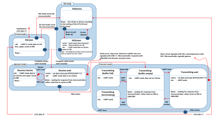
8.2.7
Synchronization in single octet UART mode
The L6364 uses a PLL (phase-locked loop) to continuously lock the UART receive and transmit frequency to the master frequency.
A few octet values (00h, 80h, e0h, f8h and feh) do not provide information which can be used to correct the PLL
frequency, and a continuous sequence of these values could prevent the PLL performing frequency tracking for some time.
In IO-Link operation, however, it is not possible to create such M-sequences as the defined format of the M-sequence, and in particular the checksum, guards against this.
A continuous sequence of these octets is possible when the single octet UART mode is used in a proprietary mode, eg. for code download.
In this case, the insertion of a synchronization octet (aah) at least every 75 ms is required, taking into account
a worst case dissipation change (1W) in combination with a worst case oscillator temperature drift. The interval
of 75 ms is equivalent to 240 octets at 38.4kBaud assuming an inter-frame delay of 1 bit. We recommend the insertion of a synchronization octet every 32 octets.
8.3
Transparent UART mode
The L6364 supports an operating mode for transparent communication of UART frames.
In this mode, the frames are received and transmitted from a UART peripheral in the microcontroller, and the function of the DUAL PHY device is reduced to that of a physical level converter.
This mode is supported by dual use of the MOSI and MISO pins, maintaining the low overall pin-count and a restricted use of microcontroller resources.
Transparent mode is entered by setting the CCTL:TRNS register bit to '1' via the SPI. In this mode the IO-Link state machine in the L6364 and the PLL are placed in reset.
The interrupt line and status monitoring for reset, short-circuit, overtemperature and undervoltage events continue to function.
page 21/60
Page 22
Transparent mode output path
8.3.1
Pin functions in transparent mode
In transparent mode, the MOSI and MISO pins are used for both SPI communication, and for the transparent path. The SS pin controls the use of the MOSI and MISO pins, according to Table 18.
Table 18. Pin dual use in transparent mode
| SPI comm’s | Transparent path | MOSI | MISO | |
| SS=’0’ | SPI comm’s active | CQ output switch control frozen | SPI data in | SPI data out |
| SS=’1’ | SPI comm’s frozen | Transparent path active | CQ output switch control | Filtered CQ line level |
An SPI communication in transparent mode is shown in Figure 9. Initially the L6364 is driving the CQ line; an SPI exchange is then conducted in which the L6364 is instructed to stop driving the line, and finally the IO-Link master drives the CQ line.
Typically the microcontroller SPI access routine records the MOSI level in use before setting SS='0' to start an SPI access, and assert this value again on the MOSI line before setting SS='1'. The microcontroller should preset the MOSI pin to the required level before the first SPI access enabling transparent mode.
Support for this may, however, be automatic depending on the microcontroller. The SPI connection to the L6364 is not suitable for a bus connection of multiple SPI slaves in transparent mode as the MOSI line is permanently driven.
Figure 9. Illustration of operation in transparent mode
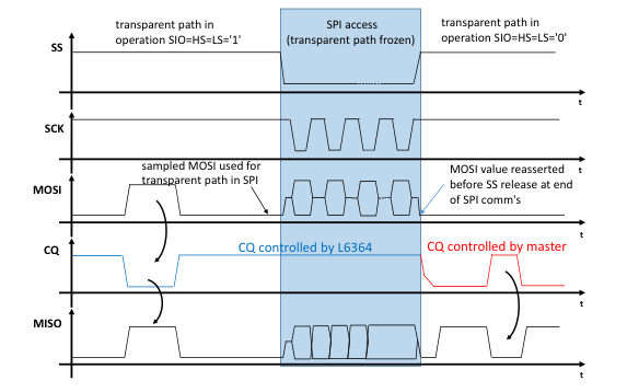
8.4
Transparent mode output path
With SS='1', the level of the MOSI pin controls the output switches according to the SIO, HS and LS bit settings as shown in Table 19. Where SS='0' for SPI access the level latched on the MOSI line is frozen, and used in the place of the MOSI line itself.
The CCTL:HS and CCTL:LS bits function as enables for the high-side and low-side switches respectively, and select operation as a high-side, low-side or push-pull device. Note that the logical path from MOSI to CQ is inverting.
page 22/60
Page 23
Transparent mode output path
Table 19. Transparent mode operation
| CCTL:SIO | CCTL:HS | CCTL:LS | Operation | Short-circuit |
| 1 | 0 | 0 | SIOListen operation | Short reported after retry |
| 1 | 0 | 1 | Low-side SIO operation | |
| 1 | 1 | 0 | High-side SIO operation | |
| 1 | 1 | 1 | Push-pull SIO operation | |
| 0 | 0 | 0 | IOListen operation | Short timers reset |
| 0 | 0 | 1 | Do not use | |
| 0 | 1 | 0 | Do not use | |
| 0 | 1 | 1 | Push-pull IO-Link operation | Short reported immediately |
In transparent SIO operation (CCTL:TRNS='1', CCTL:SIO='1') a short is only reported after N retries, see tRETRY, which is suitable to indicate the presence of a valid IO-Link wake-up pulse.
In transparent IO-Link operation (CCTL:TRNS='1', CCTL:SIO='0'), a short is reported immediately after tSHORT. In both cases the device attempts to drive the line again after tRETRY and then tRESTART without intervention from the microcontroller.
The output switches are disabled while a short is reported, protecting the device from excessive dissipation. The short condition and associated internal timers can be reset by setting IOListen operation (CCTL:TRNS='1', CCTL:SIO=CCTL:HS=CCTL:LS='0'), which allows switching to push-pull IO-Link operation after valid data has been received.
Following a cleared short condition, a new driving operation should only be selected after receiving valid IO-Link data or waiting for at least tRESTART.
8.4.1
Transparent mode input path With SS='1' in transparent mode, the level of the MISO line is the inverted level of the CQ signal. The signal is filtered with a constant delay filter, (1/16) \* TBIT, see Table 5, to remove line glitches.
8.4.2
Leaving transparent mode Transparent mode is left by clearing the CCTL:TRNS register bit to '0' via the SPI.
page 23/60
Page 24
IO-Link physical layer
9
IO-Link physical layer
9.1
UART frame
Table 20. UART frame definition
| Bit# | Significance | Level |
| 1 | START | 0 |
| 2 | LSB | b0 |
| 3 | b1 | |
| 4 | b2 | |
| 5 | b3 | |
| 6 | b4 | |
| 7 | b5 | |
| 8 | b6 | |
| 9 | MSB | b7 |
| 10 | PARITY | P |
| 11 | STOP | 1 |
A logic '1' is transmitted as a low level on the CQ line, and a logic '0' is transmitted as a high level on the line. The idle state for the CQ line is low.
Even parity is used, that is, there is always an even number of logical '1' bits in the 9 bit concatenation of the data bits b[7:0] and the parity bit.
9.2
M-sequence interpretation
The data direction is derived from the MSB of the first octet of the master message, M-sequence control (MC), where a ‘1’ denotes a read operation and a '0' a write.
Table 21. M-sequence control (MC) octet
MSB
LSB
R/W
Comm chan.
Address
The M-sequence type is derived from bits [7:6] of the second octet of the master message, “Checksum/ Msequence type” (CKT), which have permissible values of 2'b00, 2'b01, or 2'b10, and denotes whether the structure of the message is of Type 0, Type 1 or Type 2.
Table 22. Checksum/M-sequence type (CKT) octet
MSB
LSB
M-seq. type
Checksum
The total length of the received M-sequence is determined according to Table 23 and is dependent on the M-sequence type and on the transfer direction (READ or WRITE).
page 24/60
Page 25
M-sequence interpretation
Table 23. Receive M-sequence lengths
| CKT:M-seq.type [7:6] | Received M-Sequence length | ||
|---|---|---|---|
| READ, MC:R/W = '1' | WRITE, MC:R/W = '0' | ||
| Type 0 | 00 | 2 octet | 3 octet |
| Type 1 | 01 | 2 octet | 2 octet + f(OD1)* |
| Type 2 | 10 | M2CNT | M2CNT+ f(OD2) |
f(OD1), f(OD2) and M2CNT are used to configure the L6364 for M-Sequence reception and are configured through register MSEQ as follows:
- f(OD1), f(OD2): defines the received number of on-demand octets, where support is only provided for data widths of 1, 2 and 8 octets and not 32. The values are determined from MSEQ:OD1[1:0] for type 1 sequences and MSEQ:OD2[1:0] for type 2 sequences according to Table 24.
Table 24. Permissible values of MSEQ:OD1 and MSEQ:OD2
| MSEQ:OD1[1:0] | f(OD1) (On-demand data) | MSEQ:OD2[1:0] | f(OD2) (On-demand data) | |
| 00 | Illegal(*) | 00 | 1 octet | |
| 01 | 2 octet | 01 | 2 octet | |
| 10 | 8 octet | 10 | 8 octet |
- M2CNT: defines the expected octet count on a read operation. Its value corresponds to the value of field MSEQ:M2CNT[3:0]
The total data buffer size is 15 octets. If an M-sequence of a length greater than this is required for reception or transmission, then the single octet access mode should be used (see Section 8.2 ). (\*)A setting of MSEQ:OD1[1:0]=00 is used for backwards compatibility. In this case M2CNT + f(OD2) defines the length of received type 1 M-sequences.
page 25/60
Page 26
M-sequence interpretation
9.2.1
Example setting
Table 25 shows examples to illustrate the correct register settings for M2CNT, OD1 and OD2 for different combinations of PREOPERATE and OPERATE M-sequences.
Table 25. Example M2CNT, OD1 and OD2 registers setting
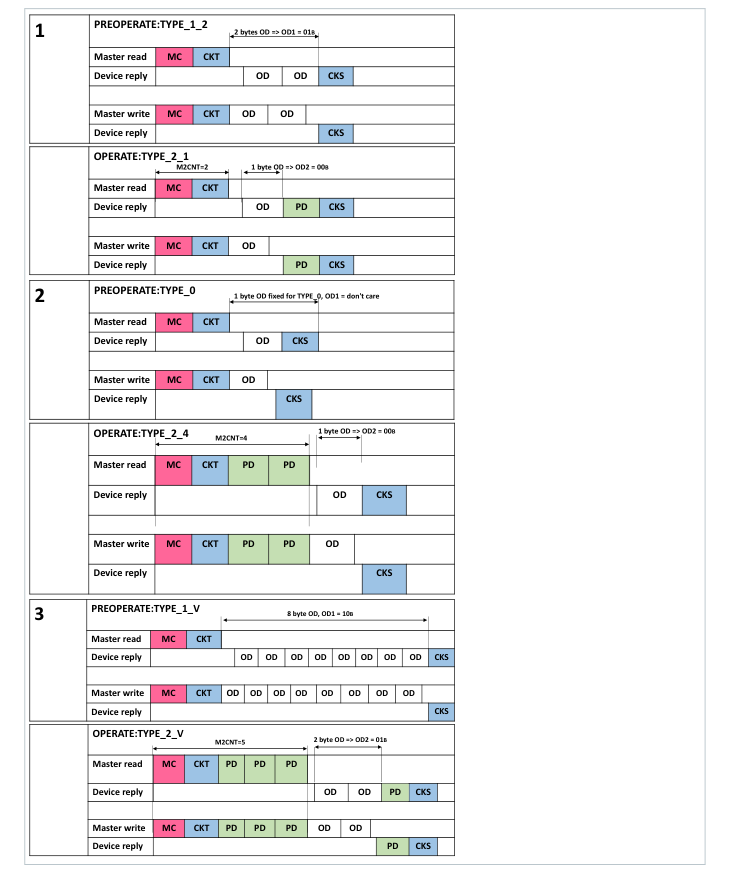
page 26/60
Page 27
Checksum calculation and verification
9.3
Checksum calculation and verification
The checksum for an out-going message is calculated by the L6364, by logically exclusively OR'ing all LINK:CNT octets of the message, with a starting value of 0x52. For this calculation the written value of the Checksum register should be zero. The Checksum is then compacted from 8 to 6 bits using the algorithm of Table 26:
Table 26. Checksum compaction
| Bit | Calculation |
| C[5] | D[7] xor D[5] xor D[3] xor D[1] |
| C[4] | D[6] xor D[4] xor D[2] xor D[0] |
| C[3] | D[7] xor D[6] |
| C[2] | D[5] xor D[4] |
| C[1] | D[3] xor D[2] |
| C[0] | D[1] xor D[0] |
The L6364 then inserts this 6-bit checksum into the lower bits of the last octet sent (“Checksum/status octet”).
Table 27. Checksum/status (CKS) octet
MSB
LSB
Event flag
PD Invalid
Checksum
The L6364 calculates the expected checksum for an incoming message, by exclusively OR'ing the octets of the message, with a starting value of 0x52. For this calculation the Checksum/M-sequence type (CKT) octet is used, but with all of the bits of the Checksum field set to zero. The calculated and expected checksum are compared and STATUS:CHK is set accordingly.
9.4
Data signal receive
The baud rate for signal reception is set by the CFG:BD bit. Both 38.4.4k Baud and 230.4k Baud are supported. The CQ data level is monitored for signals, filtering out pulses with a duration of less than (1/16) \* TBIT, see Table 5. The decision threshold for the CQ data level is determined by the CFG:RF bit.
Where this is '0', the IO-Link standard absolute levels are used, and where the bit is '1' the threshold is referred to VVPLUS/2. The first transition is the start reference of the frame. After this, data is sampled at the center of each bit time. Bits are read into the data buffer, removing the start and stop bits. The fill level is recorded in the LINK:CNT field.
Once the expected number of UART frames have been read, the checksum and parity bits for the message are checked, and the STATUS:CHK bit set appropriately. The STATUS:DAT status bit is set, and an interrupt is generated. Consecutive UART frames are expected from the master within a period of 4xTBIT. If this time is exceeded, then both STATUS:DAT and STATUS:CHK bits are set and an interrupt is generated.
The L6364 then enters the Transmit state and waits for the microcontroller to read the data and prepare a return message, signaling completion by writing a '1' to either the LINK:SND or LINK:END register bits.
9.5
Data output
The baud rate for transmission is set by the CFG:BD bit. Both 38.4.4k Baud and 230.4k Baud are supported. The number of message octets for transmission are written into the LINK:CNT field and sent following writing bit LINK:SND. The START, STOP and PARITY bits are appended to create the UART frames, and the checksum calculated and stuffed in the message.
page 27/60
Page 28
Clock recovery
The data is sent by using push-pull operation of the output switches. Writing either the LINK:SND or LINK:END bit clears the STATUS:DAT and STATUS:CHK status flags. The data output is synchronized using the internal PLL clock.
As defined in the IO-Link specification v1.1, the device has a maximum of 10xTBIT periods to process the incoming message and prepare the response. A delay of up to TBIT/16 can be incurred in the L6364 due to synchronization with the internal PLL clock, leaving the microcontroller slightly less than 10xTBIT to respond.
9.6
Clock recovery
The L6364 has an internal RC clock with a nominal frequency of fCK. The filtered data line is monitored for transitions while in the IOListen and SIOListen states.
When a first rising edge is seen, the internal PLL clock phase is aligned to the incoming data. The PLL clock corrects its operational frequency on the detection of further rising edges.
See Section 8.2.7 regarding detailed operation in single octet mode. The clock correction has a resolution of 0.4%(TYP) and a stability of 1%(MAX) over the duration of a message.
page 28/60
Page 29
Short-circuit detection
10
Short-circuit detection
In the case of short-circuit or a wake-up request from the Master, the CQ (or DIO) current exceeds the configured short-circuit threshold. If overload condition lasts longer than tSHORT (delay to filter-out any spurious transients), the output transistors of the affected output are switched off. In IO-Link mode, the event is signaled immediately to the microcontroller via the STATUS:SSC bit and an interrupt is generated. With CQ in SIO mode or with DIO in independent mode the line is reactivated with the delay tRETRY following the initial overcurrent event (see Figure 10. Wake-up time diagram). If overload is still present, then it is signaled to the microcontroller via STATUS:SSC bit and an interrupt is generated. The output stays switched-off for the time
tRESTART in order to allow reception of a valid IO-Link message or to protect the IC against overloading. If the tRESTART time elapses without intervention by the microcontroller or without reception of a valid IO-Link message, then the L6364 attempts to drive the line again. In the event of a continued overload, this cycle repeats indefinitely. The described mechanism ensures detection of an IO-Link Master wake-up request while also providing full protection of the IC in case of overload. The short-circuit current thresholds are set by CCTL:SCT[2:0] and DCTL:SCT[2:0]. Where JOIN mode is requested, the DCTL:SCT[2:0], DCTL:HS and DCTL:LS bits no longer have any effect on the output state or
short-circuit detection.
Table 28. DC short-circuit threshold current, ISET, CQ and DIO
| CCTL:SCT, DCTL:SCT | Threshold DIO/SIO | Threshold JOIN mode | CCTL:SCT, DCTL:SCT | Threshold DIO/SIO | Threshold JOIN mode |
| decimal | (mA) | (mA) | decimal | (mA) | (mA) |
| 4 | 110 | 220 | 0 | 190 | 380 |
| 5 | 130 | 260 | 1 | 210 | 420 |
| 6 | 150 | 300 | 2 | 230 | 460 |
| 7 | 170 | 340 | 3 | 250 | 500 |
Figure 10. Wake-up time diagram
page 29/60
Page 30
Maximum current output
11
Maximum current output
The switches have an independent saturation current of ISAT, and do not draw more current than this. If, however, the CQ and DIO pins are configured to create a single output (JOIN mode), then the saturation current in this case is = 2 x ISAT. The power supply must be able to supply this current for the duration tSHORT to prevent a supply voltage drop on VPLUS.
page 30/60
Page 31
Undervoltage detection
12
Undervoltage detection
If the voltage on the VPLUS is below the VUV threshold, then the status bit UV is set. An interrupt is generated if this status is different to the status reported in the last SPI exchange. The undervoltage thresholds are set by CFG:UVT[2:0].
Table 29. Undervoltage threshold
| CFG:UVT | Threshold | CFG:UVT | Threshold |
| decimal | (V) | decimal | (V) |
| 0 | 15.0 | 4 | 10.5 |
| 1 | 14.0 | 5 | 8.5 |
| 2 | 13.0 | 6 | 7.5 |
| 3 | 12.0 | 7 | 6.0 |
page 31/60
Page 32
Short term power loss
13
Short term power loss
If the supply on the VPLUS fails then reverse current from V3V3 to VPLUS and from V5V to VPLUS is blocked. A residual leakage current of IPLUSREV may still flow in this time. Appropriate dimensioning of the capacitors CV3V3 and CV5V can be used to maintain the power supply during this event.
page 32/60
Page 33
Temperature measurement
14
Temperature measurement
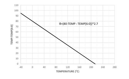
The measured temperature in Celsius can be read from the L6364 from the TEMP:TEMP[6:0] register. The temperature is given as shown in Figure 11.
Figure 11. L6364 temperature measurement
page 33/60
Page 34
Thermal shutdown
15
Thermal shutdown
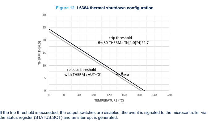
The STATUS:SOT status bit is a filtered version of the output of the temperature sensor. When the L6364 temperature exceeds the threshold this bit is set to '1', when the temperature is below the threshold the bit is set to '0'. The trip threshold is determined by the set-point in register THERM:TH[4:0] as shown in Figure 12.
15.1
Automatic operation
If the THERM:AUT bit is '0' and a temperature in excess of the set point is reached, then the threshold is automatically moved to a release threshold ΘHYST below the set point. When the temperature falls below this release threshold, the L6364 returns to a normal operating state and returns the threshold to the original level.
page 34/60
Page 35
LED outputs
16
LED outputs
Two current controlled outputs are provided to generate an LED current up to 8 mA. The nominal LED current is defined by the settings of the LED:LED1 and LED:LED2 fields.
Figure 13. L6364 LED currents
0 1 2 3 4 5 6 7 8 9 10 11 12 13 14 15
LED : LEDx [3:0]
page 35/60
Page 36
DC-DC converter
17
DC-DC converter
17.1
Converter configuration
The L6364 includes a DC-DC buck converter, which operates at a frequency configured by register DCDC:FSET[2:0], shown in Table 30. Irregular frequency steps have been carefully chosen so to avoid simple fractional multiples, such that it is possible to choose a controller frequency which does not interfere with a given sensor frequency.
Table 30. DC-DC converter nominal operating frequency, FSET
| DCDC:FSET | Frequency | DCDC:FSET | Frequency |
| [kHz] | [kHz] | ||
| 4 | 500 | 0 | 1000 |
| 5 | 625 | 1 | 1250 |
| 6 | 710 | 2 | 1670 |
| 7 | 830 | 3 | 2000 |
The output voltage on pin VDCDC is configured by DCDC:VSET[2:0], shown in Table 31. Note that where operation of the 5.0V linear regulator is required, the VDCDC output voltage must be configured to be at least VDCDC_5V_MIN.
Table 31. DC-DC output voltage, VSET
| DCDC:VSET | Target output | DCDC:VSET | target output |
| [V] | [V] | ||
| 0 | 5.0 | 4 | 7.8 |
| 1 | 5.6 | 5(1) | 8.6 |
| 2 | 6.1 | 6 | 9.6 |
| 3 | 6.8 | 7 | 10.5 |
- Default value following reset.
Changes to the output voltage via VSET are executed in steps, with a delay of tVSET for each step between VSETMIN and VSETMAX. This minimizes any over- or undershoot on VDCDC as the output voltage approaches the target value. This implies that a maximum delay of ΔtVSET can occur between this range. If the DC-DC converter is not required, the pin DOUT is externally shorted to pin VDCDC.
17.2
Converter architecture
The buck converter consists of two internal MOS switches (PMOS and NMOS), an external capacitor, CDCDC, and an inductor LDCDC. The switches operate in anti-phase and, assuming no resistive losses, the output voltage on VDCDCpin is equal to the duty ratio of the high-side switch multiplied by the input voltage (VVPLUS- VDIODE).
page 36/60
Page 37
Converter operation
Figure 14. Block diagram of DC-DC converter
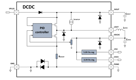
This block also includes a sense resistor (RSHUNT) to measure the inductor current, a series diode to prevent conduction during reverse polarization, and protection diodes to conduct residual inductor currents whenever switching ceases. The high-side switch is activated at the start of each cycle, and remains ON for a length of time determined by the PID controller. This block monitors the voltages at VDCDC and VPLUS pins.
17.3
Converter operation
17.3.1
Startup The converter operates only when the following operating conditions are met:
- VV3V3 >VPOR (by means, bandgap is stable)
- VVPLUS >VDCMIN (by means, oscillator toggling)
- VVPLUS>VPLUSDCMIN Operation outside these conditions is prevented to protect the IC and the surrounding circuit. Initially the converter is in a STARTUP state. In this state an internal current source attempts to source a current ISTARTUP from pin DOUT to pin LOUT. Where LOUT is connected to VDCDC by an inductor, voltage at VDCDC pin is pulled up by this current: VDCDC voltage rises until it reaches voltage VSTARTUP, where the source current is then regulated to maintain VDCDC voltage at VSTARTUP. The converter remains in the STARTUP state until the operating conditions are met. Bias is provided either by a HV bias circuit where the IC is in reset VV3V3 < VPOR, or by an LV bias circuit once V3V3 is available. During the overlap period, the bias currents are doubled.
17.3.2
Entry to operation Once the operating conditions are met, or when the DCDC:DIS bit is reset, then the converter passes through an ARM state for 1 ms before starting operation. The switch controls are powered in this state, but set to OFF.
17.3.3
Leaving operation If the operating conditions are no longer met, then the converter passes back through the ARM state to the STARTUP state. If, however, the DCDC:DIS bit is set, then the converter passes back through the ARM state to the SLEEP state. On leaving operation, any residual energy in the coil is conducted to VDCDC via the protection diode between LOUT and PGND.
page 37/60
Page 38
Converter external component consideration
17.3.4
SLEEP state The SLEEP state is reached after 1ms by setting the DCDC:DIS bit via the microcontroller. In the SLEEP state no current is drawn by the DC-DC converter on VPLUS or V3V3, and the switch control blocks are depowered. The SLEEP state is left by resetting the DCDC:DIS bit, or during a L6364 reset, that is when VV3V3 < VPOR.
17.3.5
BYPASS state The BYPASS state is equivalent to the STARTUP state, and is reached after 1 ms by setting the DCDC:BYP bit via the microcontroller. In this mode, the ISTARTUP current source is permanently enabled and the voltage on VDCDC is held at VSTARTUP. Power to the devices on the V3V3 or V5V pins is now provided via the inductor and linear regulators. Leaving the BYPASS state is achieved by clearing the DCDC:BYP bit, whereby normal operation of the DC-DC converter resumes after 40 μs. This operation mode can be used if a device is operated at times in a low current consumption state, or suppression of converter switching noise is required for a temporary period.
Converter external component consideration
17.4
17.4.1
Minimum supply voltage The DC-DC converter has a minimum off-time per cycle, which leads to a maximum duty of:
DMAX = 1 − (150 ns × fSET); eg. at fSET = 1 MHz ⇒ DMAX = 0.85.
Figure 15. Minimum supply voltage
| Minimum V VPLUS Resistive Lo | |
|---|---|
| VDIODE | |
| VSET / DMAX | |
| C | |
Voltage
VSET
0
Current
The supply voltage (VVPLUS) required to reach a nominal output voltage (VSET) is given by: VVPLUS = VSET / DMAX + VDIODE + IOUT × [RCOIL / DMAX + RHIGH + (1/DMAX−1) × (RSHUNT+ RLOW)]
For VSET= 8.6 V, VDIODE=1 V, IOUT= 50 mA, RCOIL= 2 Ω, RHIGH= RLOW= 20 Ω, RSHUNT= 1.5 Ω, DMAX= 90% a supply voltage of 11.80 V is required to ensure that the nominal set voltage can be reached for all devices over the entire temperature range.
At very low supply voltages, where the duty cycle approaches DMAX, an increased ripple on the VDCDC supply
Note:
may occur.
17.4.2
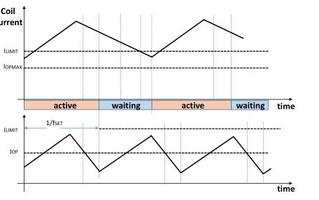
Coil current limitation protection Where the coil current exceeds ILIMIT at the start of a cycle, that cycle is aborted. The current is checked again every 200 ns and a normal cycle is started once the coil current is below ILIMIT.
page 38/60
Page 39
Converter external component consideration
This results in a constant current output behavior with a variable frequency switching (see Figure 16). The operating current and external components should be chosen to avoid this behavior under normal conditions.
Figure 16. Overcurrent operation
a) Overcurrent operation
b) Normal operation
For coil protection purposes, the maximum duty is further limited by the L6364 in relation to the supply voltage so that the maximum coil current rise in one cycle is limited to:
DMAX≾ 19.2 V / VVPLUS ⇒ Δ I ≾ 19.2V / (fSET × LCOIL)
For fSET= 1 MHz, LCOIL= 220 μH ⇒ ΔI<=87mA.
17.4.3
Capacitive blocking of DOUT CDOUT provides capacitive isolation of the VPLUS supply from the DC-DC regulator. A minimum value, see Table 5. Receiver CQ/DIO, is required to correctly supply the transient currents when the DC-DC converter switches pin LOUT, and at low output currents where there is a negative current in the coil in part of the cycle. The value may, however, be increased to provide additional isolation from input voltage ripple on VPLUS.
page 39/60
Page 40
Linear regulators
18
Linear regulators
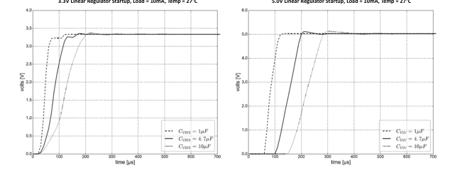
In addition to the DC-DC regulator, the L6364 includes two 50 mA linear regulators supplied from the VDCDC pin, which have internally set output levels at 3.3 V (V3V3 pin) and 5.0 V (V5V pin). The 3.3 V linear regulator acts as the master, and the 5.0 V linear regulator as the slave. The start-up time of the 5.0 V linear regulator is thus dependent on the 3.3 V level, and on the size of the 3.3 V line capacitance, CV3V3. The regulators' dynamic start-up behaviour under different conditions of load capacitance can be seen in Figure 17. A typical load of 10mA, a supply voltage of 24 V with a rise time of 2.4 V/μs on pin VPLUS were used. The core of the L6364 device is supplied by the V3V3 rail, and thus an external blocking capacitor CV3V3 for
stable operation is required and is mandatory. A maximum static load, equivalent to a resistor RSTART_MIN, may be drawn externally on V3V3 during startup. A static load is the current which would be drawn continuously by the application circuit if the output voltage, VSNS, were held at a fixed level. A load in excess of this level may block the startup. A higher dynamic load (eg. capacitor charging) is permitted. Dynamic loads affect (slow) the start, but do not block startup.
In normal operation the consumption of the L6364 itself is limited to the quiescent current, IQUIES. During startup, the static load contributed by the L6364 on the supply is limited to IQUIES_START. The actual load is increased by the current drawn to charge the application capacitors and any external loads.
Figure 17. L6364 linear regulators' startup under different conditions of load capacitance
3.3V Linear Regulator Startup, Load = 10mA, Temp = 27°C
5.0V Linear Regulator Startup, Load = 10mA, Temp = 27°C
The 5.0 V regulator output is not used internally and is provided for external use. When in use, an external blocking capacitor CV5V must be provided for stable operation, and the input supply range must be sufficient (VVPLUS > VSUP in pure mode or VDCDC > VDCDC_5V_MIN for DC-DC operation).
When the 5.0 V linear regulator is not in use, either permanently or periodically, then this block may be placed in a power-down state by setting bit CFG:PD5V. When this bit is set to '1', the 5.0 V regulator is placed in power-down and the output pin, V5V, is pulled low with a discharge current of IPD5V. This ensures capacitances on the line are discharged cleanly, and that the output is tied to a known state.
page 40/60
Page 41
Power dissipation
19
Power dissipation
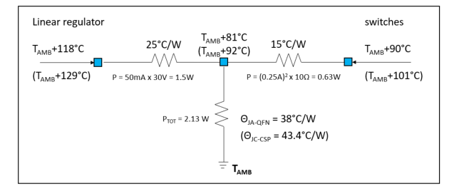
Figure 18 shows an example how to estimate the device junction temperatures based on the dissipation of the regulator and switches. Since the thermal performance in the final application is dependant on a number of factors (e.g. PCB design, power dissipation of neighbouring components, ambient temperature, air flow. bumppitch etc), the thermal package properties provided in the figure below should only serve as a guideline. cc
Figure 18. Example of thermal power dissipation estimation
The maximum average power consumption per channel (CQ or DIO) in short-circuit is:
ISAT(MAX) × VVPLUS(MAX)× tSHORT × NRETRY / tRESTART = 13.4 mW
In case of inductive load, the power dissipation (assuming no internal losses in the inductor itself) is : P = 1 2 fSW × L × I2 , where fSW is the switching frequency, L the load inductance and I the operating current. The design of the application hardware (heat-sink capability) should take account of this heating.
page 41/60
Page 42
Surge pulse and reverse polarity protections
Surge pulse and reverse polarity protections
20
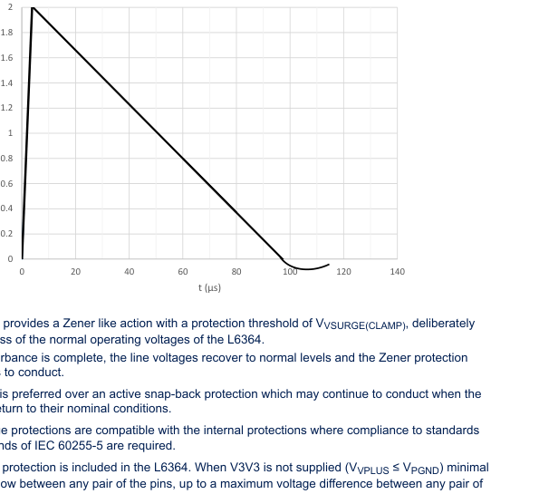
The PGND, CQ, DIO and VPLUS pins are fully protected by a surge protection, to withstand an asymmetric surge between any pair of these pins according to IEC 60255-5, i.e. > 2 APK (up to 3 APK) for a half-time of 50 μs. Note that the surge stimulus is applied between the pins, rather than in common mode. This subjects the device under test to the current ratings shown in Figure 19.
Figure 19. Surge waveform
automatically ceases to conduct.
operating voltages return to their nominal conditions.
exceeding the demands of IEC 60255-5 are required.
pins of 35 V.
if the L6364 is rapidly switched from a correctly polarized condition to a reverse polarized condition, such that
Note:
the CV3V3 capacitor remains charged, then the Zener function of the CQ output causes a destructive current to flow.
Sufficient time should be allowed (ms) during testing of the reverse polarization function to allow CV3V3 to discharge.
page 42/60
Page 43
Register Map
21
Register Map
Table 32. Register map
| Register name | Register address | BIT 7 | BIT 6 | BIT 5 | BIT 4 | BIT 3 | BIT 2 | BIT 1 | BIT 0 |
| MSEQ | 0x00 | R/W | R/W | R/W | R/W | R/W | R/W | R/W | R/W |
| OD1[1] | OD1[0] | M2CNT[3] | M2CNT[2] | M2CNT[1] | M2CNT[0] | OD2[1] | OD2[0] | ||
| 00: Backwards compatibility | expected octet count on read | 00: 1 octet on-demand data | |||||||
| 01: 2 octets on-demand data | 01: 2 octets on-demand data | ||||||||
| 10: 8 octets on-demand data | 10: 8 octets on-demand data | ||||||||
| 11: reserved | 11: reserved | ||||||||
| type 1 | type 2 | ||||||||
| CFG | 0x01 | R/W | R/W | R/W | R/W | R/W | R/W | R | R |
| UVT[2] | UVT[1] | UVT[0] | BD | RF | PD5V | 0 | 0 | ||
| Set UVLO signalization threshold, see Table 29. Undervoltage threshold | 0: Baud rate = 38.4 kbaud | 0: absolute CQ/DIO comparato r ref. level | 0: 5V regulator active | N/A | N/A | ||||
| 1: Baud rate = 230.4 kbaud | 1: CQ/DIO comparato r ref. level at VVPLUS/1. 8 | 1: 5V regulator inactive | |||||||
| CCTL | 0x02 | R/W | R/W | R/W | R/W | R/W | R/W | R/W | R/W |
| TRNS | SCT[2] | SCT[1] | SCT[0] | SGL | SIO | HS | LS | ||
| 1: set transparen t mode | Set overcurrent signalization level, see Table 28. DC short-circuit threshold current, ISET, CQ and DIO | 1: Single octet UART mode | 1: SIO mode requested | 1: enables CQ HS switch | 1: enables CQ LS switch | ||||
| DCTL | 0x03 | R/W | R/W | R/W | R/W | R/W | R/W | R/W | R/W |
| EXT | SCT[2] | SCT[1] | SCT[0] | IEN | DIO | HS | LS | ||
| 1: enable use of CTLD pin | Set overcurrent signalization level, see Table 28. DC short-circuit threshold current, ISET, CQ and DIO | 1: Level change interrupt enable | 1: DIO mode requested | 1: enables DIO HS switch | 1: enables DIO LS switch | ||||
| LINK | 0x04 | R | R | R/W | R/W | R/W | R/W | W | W |
| 0 | 0 | CNT [3] | CNT [2] | CNT [1] | CNT [0] | END | SND | ||
page 43/60
Page 44
Register Map
| Register name | Register address | BIT 7 | BIT 6 | BIT 5 | BIT 4 | BIT 3 | BIT 2 | BIT 1 | BIT 0 |
| LINK | 0x04 | N/A | N/A | Data buffer fill count(1). | 1: declines sending response | 1: sends IO- Link respo nse immediatel y | |||
| THERM | 0x05 | R/W | R | R | R/W | R/W | R/W | R/W | R/W |
| AUT | 0 | 0 | TH [4] | TH [3] | TH [2] | TH [1] | TH [0] | ||
| 0: automatic thermal control on | N/A | N/A | Set thermal shutdown threshold see Figure 12. L6364 thermal shutdown configuration | ||||||
| 1: automatic thermal control off | |||||||||
| TEMP | 0x06 | R | R | R | R | R | R | R | R |
| 0 | TEMP [6] | TEMP [5] | TEMP [4] | TEMP [3] | TEMP [2] | TEMP [1] | TEMP [0] | ||
| N/A | IC internal temperature see Figure 11. L6364 temperature measurement | ||||||||
| LED | 0x07 | R/W | R/W | R/W | R/W | R/W | R/W | R/W | R/W |
| LED1 [3] | LED1 [2] | LED1 [1] | LED1 [0] | LED2 [3] | LED2 [2] | LED2 [1] | LED2 [0] | ||
| See Figure 13. L6364 LED currents | |||||||||
| DCDC | 0x08 | R/W | R/W | R/W | R/W | R/W | R/W | R/W | R/W |
| DIS | BYP | FSET [2] | FSET [1] | FSET [0] | VSET [2] | VSET [1] | VSET [0] | ||
| 1: Disable DC-DC converter | 1: Bypass DC-DC converter | Set DC-DC switching frequency, see Table 30. DC-DC converter nominal operating frequency, FSET | Set DC-DC output voltage, see Table 31. DC-DC output voltage, VSET | ||||||
| DSTAT | 0x09 | R | R | R | R | R | R | R | R |
| 1 | 0 | 0 | 0 | 0 | LVL | SSC | 0 | ||
| N/A | N/A | N/A | N/A | N/A | 1: DIO Line level | 1: Short circuit triggered | N/A | ||
| STATUS | 0x0A | R/W | R | R | R | R | R | R | R |
| RST | INT | UV | DINT | CHK | DAT | SSC | SOT | ||
| 0: following reset even t | 1: when interrupt active prior to SPI read | 1: UVLO triggered | 1: DIO interrupt triggered | 1: checksum or parity error triggered | 1: IO-Link machine waiting to transmit | 1: Short circuit triggered | 1: Over- temperatur e triggered | ||
| 1: set by writing this bit | |||||||||
| LINK2(2) | 0x0F | R | R | R/W | R/W | R/W | R/W | W | W |
| 0 | 0 | CNT [3] | CNT [2] | CNT [1] | CNT [0] | END | SND | ||
page 44/60
Page 45
Register Map
| Register name | Register address | BIT 7 | BIT 6 | BIT 5 | BIT 4 | BIT 3 | BIT 2 | BIT 1 | BIT 0 |
| LINK2(2) | 0x0F | N/A | N/A | Data buffer fill count(3). | Writing '1' declines sending response | Writing '1' sends IO- Link response after FR0 is written | |||
| FR0 to FR14 | 0x10 to 0x1E | R/W | R/W | R/W | R/W | R/W | R/W | R/W | R/W |
| DATA [7] | DATA [6] | DATA [5] | DATA [4] | DATA [3] | DATA [2] | DATA [1] | DATA [0] | ||
| The data buffer registers are only accessible when frame data is available (DAT bit set).The initial value of all register bits following reset is '0', except bits DCDC:VSET[2:0], where the default value is 5. | |||||||||
- Valid CNT data may only be read when data is available (DAT bit set). If this is true, then reading the field returns the number received octets. Writing the CNT field sets the number of octets to transmit. Note that a read back will continue to read the number of octets in the received frame, and not the value written over SPI. 2. LINK register repeated prior to frame buffer with deferred send function 3. Valid CNT data may only be read when data is available (DAT bit set). If this is true, then reading the field returns the number received octets. Writing the CNT field sets the number of octets to transmit. Note that a read back will continue to
read the number of octets in the received frame, and not the value written over SPI.
page 45/60
Page 46
Detailed block diagram
22
Detailed block diagram
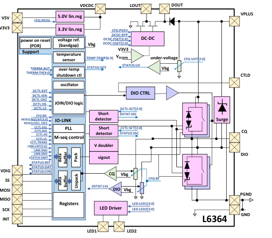
Figure 20 shows the details of the internal blocks of the L6364, and indicates which blocks the register fields act on, or are generated by.
Figure 20. Detailed block diagram, showing register field connections
page 46/60
Page 47
Typical Applications
23
Typical Applications
Figure 21. Application example: DC-DC disabled, CQ and DIO coupled (Join Mode), VSENSOR = 5 V, VMCU =
VDIG = 3.3 V
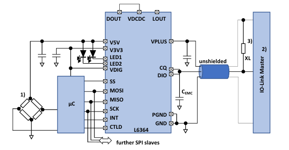
1) AFE (sensor) 2) IO-Link master is used for IO-Link mode and device configuration 3) XL (high or low-side) in Single Input Output mode
Figure 22. Application example: DC-DC enabled, CQ and DIO coupled (Join Mode), VSENSOR = VMCU =
VDIG = 5.0 V
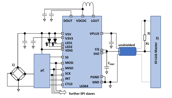
1) AFE (sensor) 2) IO-Link master is used for IO-Link mode and device configuration 3) XL (high or low-side) in Single Input Output mode
page 47/60
Page 48
Typical Applications
Figure 23. Application example: DC-DC disabled, CQ as line driver, DIO as load driver, VSENSOR = 5.0 V,
VMCU = VDIG = 3.3 V
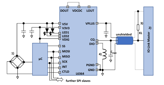
1) AFE (sensor) 2) IO-Link master is used for IO-Link mode and device configuration 3) XL (high or low-side) in Single Input Output mode 4) Industrial Load (e.g. Valve)
Figure 24. Application example: DC-DC enabled, CQ and DIO as independent line drivers, VSENSOR > 5.0 V,
VMCU = VDIG = 5.0 V
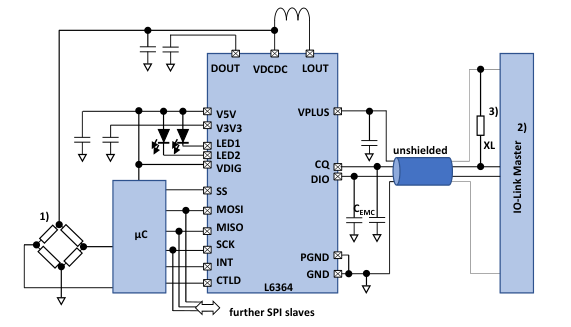
1) AFE (sensor) 2) IO-Link master is used for IO-Link mode and device configuration 3) XL (high or low-side) in Single Input Output mode 4) Industrial Load (e.g. Valve)
page 48/60
Page 49
QFN20L Package and Packing Mechanical Data
QFN20L Package and Packing Mechanical Data
24
In order to meet environmental requirements, ST offers these devices in ECOPACK® packages. These packages have a Lead-free second level interconnect. The category of second level interconnect is marked on the package and on the inner box label, in compliance with JEDEC Standard JESD97. The maximum ratings related to soldering conditions are also marked on the inner box label. ECOPACK is an ST trademark. ECOPACK specifications are available at: www.st.com
Figure 25. QFN20L mechanical drawings
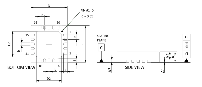
Table 33. QFN20L Dimensions [mm]
| SYMBOL | MIN. | TYP. | MAX. |
|---|---|---|---|
| A | 0.80 | 0.90 | 1.00 |
| A1 | 0.02 | ||
| A2 | 0.65 | 1.00 | |
| A3 | 0.25 | ||
| b | 0.18 | 0.23 | 0.30 |
| D | 3.85 | 4.00 | 4.15 |
| D2 | 2.60 | 2.70 | 2.80 |
| E | 3.85 | 4.00 | 4.15 |
| E2 | 2.60 | 2.70 | 2.80 |
| e | 0.45 | 0.50 | 0.55 |
| L | 0.30 | 0.40 | 0.50 |
| ddd | 0.08 |
page 49/60
Page 50
QFN20L Package and Packing Mechanical Data
Figure 26. QFN20L Suggested footprint
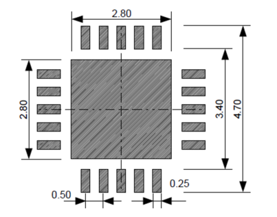
Figure 27. QFN20L, Packing information (drawing and dimension [mm])
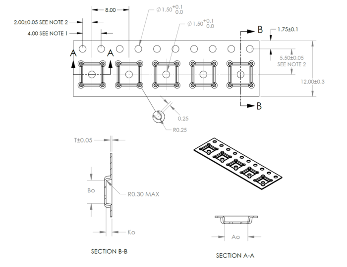
1: 10 SPROCKET HOLE PITCH CUMULATIVE TOLERANCE ±0.2
Note:
2: POCKET POSITION RELATIVE TO SPROCKET HOLE MEASURED AS TRUE POSITION OF POCKET, NOTPOCKET HOLE.
page 50/60
Page 51
QFN20L Package and Packing Mechanical Data
Table 34. QFN20L, Packing information (additional dimension info [mm])
| SYMBOL | MIN. | TYP. | MAX. |
|---|---|---|---|
| Ao | 4.25 | 4.35 | 4.45 |
| Bo | 4.25 | 4.35 | 4.45 |
| Ko | 1.0 | 1.1 | 1.2 |
| T | 0.25 | 0.3 | 0.35 |
page 51/60
Page 52
CSP19 Package and Packaging Mechanical Data
CSP19 Package and Packaging Mechanical Data
25
In order to meet environmental requirements, ST offers these devices in ECOPACK® packages. These packages have a Lead-free second level interconnect. The category of second level interconnect is marked on the package and on the inner box label, in compliance with JEDEC Standard JESD97. The maximum ratings related to soldering conditions are also marked on the inner box label. ECOPACK is an ST trademark. ECOPACK specifications are available at: www.st.com
Figure 28. CSP19 Mechanical drawings
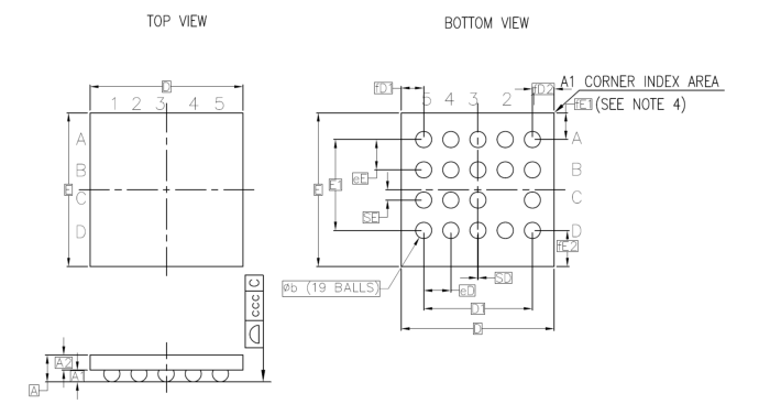
Table 35. CSP19 Dimensions [mm]
| SYMBOL | MIN. | TYP. | MAX. |
|---|---|---|---|
| A | 0.414 | 0.444 | 0.474 |
| A1 | 0.179 | 0.194 | 0.209 |
| A2 | 0.225 | 0.250 | 0.275 |
| b | 0.239 | 0.269 | 0.299 |
| D | 2.507 | 2.537 | 2.567 |
| E | 2.507 | 2.537 | 2.567 |
| D1 | 1.8 BSC | ||
| E1 | 1.5 BSC | ||
| eD | 0.45 BSC | ||
| eE | 0.50 BSC | ||
| SD | 0.006 BSC | ||
| SE | 0.172 BSC | ||
| fD1 | 0.374 BSC | ||
| fD2 | 0.363 BSC | ||
| fE1 | 0.441 BSC | ||
page 52/60
Page 53
CSP19 Package and Packaging Mechanical Data
| SYMBOL | MIN. | TYP. | MAX. |
|---|---|---|---|
| fE2 | 0.596 BSC | ||
| ccc | 0.05 BSC | ||
Figure 29. CSP19 Suggested footprint
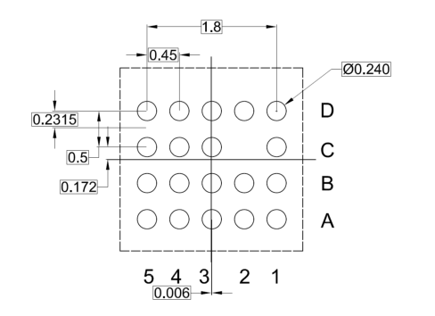
Figure 30. CSP19, Packing Information (drawing and dimension [mm])
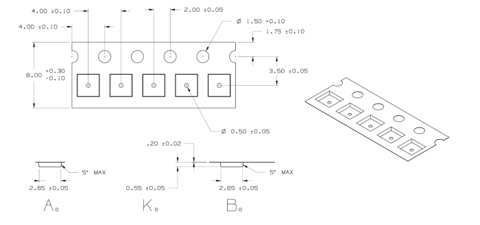
page 53/60
Page 54
Revision history
Table 36. Document revision history
| Date | Version | Changes |
| 11-Aug-2020 | 1 | Initial release. |
| 21-Oct-2020 | 2 | Replaced Figure 1, Figure 2, Section 21 , Section 21 , Figure 20, Figure 21 and Figure 22 added Figure 23 and Figure 24. |
| 30-Jul-2021 | 3 | Added CSP information: front page, package pin-out and pin description Section 3 , thermal data Section 4.2 , mechanical drawings Section 24 and packing information Section 24 . Added the maximum value for CDOUT Section 4.3 . Wake-up detection: changed NRETRY to NSHORT symbol in Table 6 Section 4.4 ; added Figure 3 and rephrased chapter 9 Section 10 . Surge protection: reworked information in Table 9 Section 4.4 with VSURGE(LEAKAGE) and VSURGE(THRESHOLD) parameters. Reworked register map style of Table 32 Section 21 . |
| 25-Oct-2021 | 4 | In front page, added packing information in Product summary table. Extended product description and moved from front page to chapter 1. Deleted VDCDC_3V3_MIN from Table 4. Recommended operating conditions. Added note about VDIG voltage rail compatibility in table Section 3 Package and pin-out and in Section 6 SPI Communication. Added RTH(JA) in JEDEC conditions in Section 4.2 Thermal Characteristics. Rephrased description of Join and DIO modes in chapter 6 Section 7 DIO pin. Rephrased chapters Section 8.1.8 Interrupt handler structure and Section 8.2.2 Receive mode Fixed input voltage value in Section 17.2 Converter architecture. Updated chapter Section 19 Power dissipation and Figure 18. Example of thermal power dissipation estimation. Updated packing information of QFN20L (Figure 27. QFN20L, Packing information (drawing and dimension [mm])) and CSP19 (Section 24 ). |
page 54/60
Page 55
Contents
Contents
1 Description . . . . . . . . . . . . . . . . . . . . . . . . . . . . . . . . . . . . . . . . . . . . . . . . . . . . . . . . . . . . . . . . . . . . . . . .2
2 Block Diagram. . . . . . . . . . . . . . . . . . . . . . . . . . . . . . . . . . . . . . . . . . . . . . . . . . . . . . . . . . . . . . . . . . . . .3
3 Package and pin-out. . . . . . . . . . . . . . . . . . . . . . . . . . . . . . . . . . . . . . . . . . . . . . . . . . . . . . . . . . . . . . .4
4 Technical Data. . . . . . . . . . . . . . . . . . . . . . . . . . . . . . . . . . . . . . . . . . . . . . . . . . . . . . . . . . . . . . . . . . . . .6
4.1 Absolute Maximum Ratings . . . . . . . . . . . . . . . . . . . . . . . . . . . . . . . . . . . . . . . . . . . . . . . . . . . . . . 6
4.2 Thermal Characteristics . . . . . . . . . . . . . . . . . . . . . . . . . . . . . . . . . . . . . . . . . . . . . . . . . . . . . . . . . 6
4.3 Recommended operating conditioning . . . . . . . . . . . . . . . . . . . . . . . . . . . . . . . . . . . . . . . . . . . . . 6
4.4 Electrical Characteristics . . . . . . . . . . . . . . . . . . . . . . . . . . . . . . . . . . . . . . . . . . . . . . . . . . . . . . . . 7
5 Startup . . . . . . . . . . . . . . . . . . . . . . . . . . . . . . . . . . . . . . . . . . . . . . . . . . . . . . . . . . . . . . . . . . . . . . . . . . .11
6 SPI Communication. . . . . . . . . . . . . . . . . . . . . . . . . . . . . . . . . . . . . . . . . . . . . . . . . . . . . . . . . . . . . . .12
6.1 Multiple byte exchange. . . . . . . . . . . . . . . . . . . . . . . . . . . . . . . . . . . . . . . . . . . . . . . . . . . . . . . . .12
7 DIO pin . . . . . . . . . . . . . . . . . . . . . . . . . . . . . . . . . . . . . . . . . . . . . . . . . . . . . . . . . . . . . . . . . . . . . . . . . . .14
7.1 DIO mode output control . . . . . . . . . . . . . . . . . . . . . . . . . . . . . . . . . . . . . . . . . . . . . . . . . . . . . . .14
7.2 SIO mode control . . . . . . . . . . . . . . . . . . . . . . . . . . . . . . . . . . . . . . . . . . . . . . . . . . . . . . . . . . . . .15
8 IO-Link UART peripheral . . . . . . . . . . . . . . . . . . . . . . . . . . . . . . . . . . . . . . . . . . . . . . . . . . . . . . . . . .16
8.1 Multi-octet UART mode . . . . . . . . . . . . . . . . . . . . . . . . . . . . . . . . . . . . . . . . . . . . . . . . . . . . . . . .16
SIO Mode . . . . . . . . . . . . . . . . . . . . . . . . . . . . . . . . . . . . . . . . . . . . . . . . . . . . . . . . . . . . . 16 8.1.1
IO-Link mode . . . . . . . . . . . . . . . . . . . . . . . . . . . . . . . . . . . . . . . . . . . . . . . . . . . . . . . . . . 16 8.1.2
Transmit mode . . . . . . . . . . . . . . . . . . . . . . . . . . . . . . . . . . . . . . . . . . . . . . . . . . . . . . . . . 16 8.1.3
IO-Link UART peripheral (Multi-octet mode) state machine. . . . . . . . . . . . . . . . . . . . . . . . 17 8.1.4
Interrupt handling . . . . . . . . . . . . . . . . . . . . . . . . . . . . . . . . . . . . . . . . . . . . . . . . . . . . . . . 17 8.1.5
Data interrupt handling . . . . . . . . . . . . . . . . . . . . . . . . . . . . . . . . . . . . . . . . . . . . . . . . . . . 18 8.1.6
Short-circuit, overtemperature and undervoltage interrupt handling . . . . . . . . . . . . . . . . . 18 8.1.7
Interrupt handler structure. . . . . . . . . . . . . . . . . . . . . . . . . . . . . . . . . . . . . . . . . . . . . . . . . 18 8.1.8
Changing to and from SIO mode. . . . . . . . . . . . . . . . . . . . . . . . . . . . . . . . . . . . . . . . . . . . 18 8.1.9
8.1.10 SPI register writes outside interrupt service routines. . . . . . . . . . . . . . . . . . . . . . . . . . . . . 19
8.2 Single octet UART mode . . . . . . . . . . . . . . . . . . . . . . . . . . . . . . . . . . . . . . . . . . . . . . . . . . . . . . .19
Buffering . . . . . . . . . . . . . . . . . . . . . . . . . . . . . . . . . . . . . . . . . . . . . . . . . . . . . . . . . . . . . . 19 8.2.1
Receive mode. . . . . . . . . . . . . . . . . . . . . . . . . . . . . . . . . . . . . . . . . . . . . . . . . . . . . . . . . . 19 8.2.2
Transmit mode . . . . . . . . . . . . . . . . . . . . . . . . . . . . . . . . . . . . . . . . . . . . . . . . . . . . . . . . . 20 8.2.3
page 55/60
Page 56
Contents
Timing errors in transmit . . . . . . . . . . . . . . . . . . . . . . . . . . . . . . . . . . . . . . . . . . . . . . . . . . 20 8.2.4
Error condition in transmit . . . . . . . . . . . . . . . . . . . . . . . . . . . . . . . . . . . . . . . . . . . . . . . . . 20 8.2.5
Single octet UART mode state machine . . . . . . . . . . . . . . . . . . . . . . . . . . . . . . . . . . . . . . 21 8.2.6
Synchronization in single octet UART mode . . . . . . . . . . . . . . . . . . . . . . . . . . . . . . . . . . . 21 8.2.7
8.3 Transparent UART mode . . . . . . . . . . . . . . . . . . . . . . . . . . . . . . . . . . . . . . . . . . . . . . . . . . . . . . .21
Pin functions in transparent mode . . . . . . . . . . . . . . . . . . . . . . . . . . . . . . . . . . . . . . . . . . 22 8.3.1
8.4 Transparent mode output path . . . . . . . . . . . . . . . . . . . . . . . . . . . . . . . . . . . . . . . . . . . . . . . . . .22
Transparent mode input path . . . . . . . . . . . . . . . . . . . . . . . . . . . . . . . . . . . . . . . . . . . . . . 23 8.4.1
Leaving transparent mode. . . . . . . . . . . . . . . . . . . . . . . . . . . . . . . . . . . . . . . . . . . . . . . . . 23 8.4.2
9 IO-Link physical layer. . . . . . . . . . . . . . . . . . . . . . . . . . . . . . . . . . . . . . . . . . . . . . . . . . . . . . . . . . . . .24
9.1 UART frame. . . . . . . . . . . . . . . . . . . . . . . . . . . . . . . . . . . . . . . . . . . . . . . . . . . . . . . . . . . . . . . . . .24
9.2 M-sequence interpretation . . . . . . . . . . . . . . . . . . . . . . . . . . . . . . . . . . . . . . . . . . . . . . . . . . . . . .24
Example setting . . . . . . . . . . . . . . . . . . . . . . . . . . . . . . . . . . . . . . . . . . . . . . . . . . . . . . . . 26 9.2.1
9.3 Checksum calculation and verification . . . . . . . . . . . . . . . . . . . . . . . . . . . . . . . . . . . . . . . . . . . .27
9.4 Data signal receive . . . . . . . . . . . . . . . . . . . . . . . . . . . . . . . . . . . . . . . . . . . . . . . . . . . . . . . . . . . .27
9.5 Data output . . . . . . . . . . . . . . . . . . . . . . . . . . . . . . . . . . . . . . . . . . . . . . . . . . . . . . . . . . . . . . . . . .27
9.6 Clock recovery. . . . . . . . . . . . . . . . . . . . . . . . . . . . . . . . . . . . . . . . . . . . . . . . . . . . . . . . . . . . . . . .28
10 Short-circuit detection . . . . . . . . . . . . . . . . . . . . . . . . . . . . . . . . . . . . . . . . . . . . . . . . . . . . . . . . . . . .29
11 Maximum current output. . . . . . . . . . . . . . . . . . . . . . . . . . . . . . . . . . . . . . . . . . . . . . . . . . . . . . . . . .30
12 Undervoltage detection . . . . . . . . . . . . . . . . . . . . . . . . . . . . . . . . . . . . . . . . . . . . . . . . . . . . . . . . . . .31
13 Short term power loss . . . . . . . . . . . . . . . . . . . . . . . . . . . . . . . . . . . . . . . . . . . . . . . . . . . . . . . . . . . .32
14 Temperature measurement . . . . . . . . . . . . . . . . . . . . . . . . . . . . . . . . . . . . . . . . . . . . . . . . . . . . . . .33
15 Thermal shutdown. . . . . . . . . . . . . . . . . . . . . . . . . . . . . . . . . . . . . . . . . . . . . . . . . . . . . . . . . . . . . . . .34
15.1 Automatic operation . . . . . . . . . . . . . . . . . . . . . . . . . . . . . . . . . . . . . . . . . . . . . . . . . . . . . . . . . . .34
16 LED outputs . . . . . . . . . . . . . . . . . . . . . . . . . . . . . . . . . . . . . . . . . . . . . . . . . . . . . . . . . . . . . . . . . . . . . .35
17 DC-DC converter . . . . . . . . . . . . . . . . . . . . . . . . . . . . . . . . . . . . . . . . . . . . . . . . . . . . . . . . . . . . . . . . .36
17.1 Converter configuration . . . . . . . . . . . . . . . . . . . . . . . . . . . . . . . . . . . . . . . . . . . . . . . . . . . . . . . .36
17.2 Converter architecture . . . . . . . . . . . . . . . . . . . . . . . . . . . . . . . . . . . . . . . . . . . . . . . . . . . . . . . . .36
17.3 Converter operation . . . . . . . . . . . . . . . . . . . . . . . . . . . . . . . . . . . . . . . . . . . . . . . . . . . . . . . . . . .37
17.3.1 Startup . . . . . . . . . . . . . . . . . . . . . . . . . . . . . . . . . . . . . . . . . . . . . . . . . . . . . . . . . . . . . . . 37
17.3.2 Entry to operation . . . . . . . . . . . . . . . . . . . . . . . . . . . . . . . . . . . . . . . . . . . . . . . . . . . . . . . 37
page 56/60
Page 57
Contents
17.3.3 Leaving operation . . . . . . . . . . . . . . . . . . . . . . . . . . . . . . . . . . . . . . . . . . . . . . . . . . . . . . . 37
17.3.4 SLEEP state . . . . . . . . . . . . . . . . . . . . . . . . . . . . . . . . . . . . . . . . . . . . . . . . . . . . . . . . . . . 38
17.3.5 BYPASS state. . . . . . . . . . . . . . . . . . . . . . . . . . . . . . . . . . . . . . . . . . . . . . . . . . . . . . . . . . 38
17.4 Converter external component consideration . . . . . . . . . . . . . . . . . . . . . . . . . . . . . . . . . . . . . .38
17.4.1 Minimum supply voltage . . . . . . . . . . . . . . . . . . . . . . . . . . . . . . . . . . . . . . . . . . . . . . . . . . 38
17.4.2 Coil current limitation protection . . . . . . . . . . . . . . . . . . . . . . . . . . . . . . . . . . . . . . . . . . . . 38
17.4.3 Capacitive blocking of DOUT . . . . . . . . . . . . . . . . . . . . . . . . . . . . . . . . . . . . . . . . . . . . . . . 39
18 Linear regulators . . . . . . . . . . . . . . . . . . . . . . . . . . . . . . . . . . . . . . . . . . . . . . . . . . . . . . . . . . . . . . . . .40
19 Power dissipation . . . . . . . . . . . . . . . . . . . . . . . . . . . . . . . . . . . . . . . . . . . . . . . . . . . . . . . . . . . . . . . .41
20 Surge pulse and reverse polarity protections. . . . . . . . . . . . . . . . . . . . . . . . . . . . . . . . . . . . . .42
21 Register Map . . . . . . . . . . . . . . . . . . . . . . . . . . . . . . . . . . . . . . . . . . . . . . . . . . . . . . . . . . . . . . . . . . . . .43
22 Detailed block diagram . . . . . . . . . . . . . . . . . . . . . . . . . . . . . . . . . . . . . . . . . . . . . . . . . . . . . . . . . . .46
23 Typical Applications . . . . . . . . . . . . . . . . . . . . . . . . . . . . . . . . . . . . . . . . . . . . . . . . . . . . . . . . . . . . . .47
24 QFN20L Package and Packing Mechanical Data . . . . . . . . . . . . . . . . . . . . . . . . . . . . . . . . . . .49
25 CSP19 Package and Packaging Mechanical Data . . . . . . . . . . . . . . . . . . . . . . . . . . . . . . . . . .52
Revision history . . . . . . . . . . . . . . . . . . . . . . . . . . . . . . . . . . . . . . . . . . . . . . . . . . . . . . . . . . . . . . . . . . . . . . .54
Contents . . . . . . . . . . . . . . . . . . . . . . . . . . . . . . . . . . . . . . . . . . . . . . . . . . . . . . . . . . . . . . . . . . . . . . . . . . . . . .55
List of tables . . . . . . . . . . . . . . . . . . . . . . . . . . . . . . . . . . . . . . . . . . . . . . . . . . . . . . . . . . . . . . . . . . . . . . . . . .58
List of figures. . . . . . . . . . . . . . . . . . . . . . . . . . . . . . . . . . . . . . . . . . . . . . . . . . . . . . . . . . . . . . . . . . . . . . . . . .59
page 57/60
Page 58
List of tables
List of tables
Table 1. Pin Description . . . . . . . . . . . . . . . . . . . . . . . . . . . . . . . . . . . . . . . . . . . . . . . . . . . . . . . . . . . . . . . . . . . . . 5 Table 2. Absolute maximum ratings . . . . . . . . . . . . . . . . . . . . . . . . . . . . . . . . . . . . . . . . . . . . . . . . . . . . . . . . . . . . . 6 Table 3. Thermal data. . . . . . . . . . . . . . . . . . . . . . . . . . . . . . . . . . . . . . . . . . . . . . . . . . . . . . . . . . . . . . . . . . . . . . . 6 Table 4. Recommended operating conditions. . . . . . . . . . . . . . . . . . . . . . . . . . . . . . . . . . . . . . . . . . . . . . . . . . . . . . . 6 Table 5. Receiver CQ/DIO. . . . . . . . . . . . . . . . . . . . . . . . . . . . . . . . . . . . . . . . . . . . . . . . . . . . . . . . . . . . . . . . . . . . 7
Table 6. Short-circuit and Wake-up detection . . . . . . . . . . . . . . . . . . . . . . . . . . . . . . . . . . . . . . . . . . . . . . . . . . . . . . . 8 Table 7. POR (Power On Reset) . . . . . . . . . . . . . . . . . . . . . . . . . . . . . . . . . . . . . . . . . . . . . . . . . . . . . . . . . . . . . . . 8 Table 8. Output switches individual channels CQ/DIO . . . . . . . . . . . . . . . . . . . . . . . . . . . . . . . . . . . . . . . . . . . . . . . . . 8 Table 9. Line surge protection, parameters with respect to any pair PGND, CQ, DIO, VPLUS . . . . . . . . . . . . . . . . . . . . . . 9 Table 10. Thermal shutdown . . . . . . . . . . . . . . . . . . . . . . . . . . . . . . . . . . . . . . . . . . . . . . . . . . . . . . . . . . . . . . . . . . . 9
Table 11. Digital pins . . . . . . . . . . . . . . . . . . . . . . . . . . . . . . . . . . . . . . . . . . . . . . . . . . . . . . . . . . . . . . . . . . . . . . . . 9 Table 12. LED Driver . . . . . . . . . . . . . . . . . . . . . . . . . . . . . . . . . . . . . . . . . . . . . . . . . . . . . . . . . . . . . . . . . . . . . . . . 9 Table 13. Linear regulators . . . . . . . . . . . . . . . . . . . . . . . . . . . . . . . . . . . . . . . . . . . . . . . . . . . . . . . . . . . . . . . . . . . . 9 Table 14. DC-DC supply . . . . . . . . . . . . . . . . . . . . . . . . . . . . . . . . . . . . . . . . . . . . . . . . . . . . . . . . . . . . . . . . . . . . . 10
Table 15. L6364 Reset conditions . . . . . . . . . . . . . . . . . . . . . . . . . . . . . . . . . . . . . . . . . . . . . . . . . . . . . . . . . . . . . . 11 Table 16. DIO control via SPI-DCTL:EXT=’0’ . . . . . . . . . . . . . . . . . . . . . . . . . . . . . . . . . . . . . . . . . . . . . . . . . . . . . . 14 Table 17. Direct DIO control via pin CTLD – DCTL:EXT=’1’ . . . . . . . . . . . . . . . . . . . . . . . . . . . . . . . . . . . . . . . . . . . . . 14 Table 18. Pin dual use in transparent mode. . . . . . . . . . . . . . . . . . . . . . . . . . . . . . . . . . . . . . . . . . . . . . . . . . . . . . . . 22 Table 19. Transparent mode operation . . . . . . . . . . . . . . . . . . . . . . . . . . . . . . . . . . . . . . . . . . . . . . . . . . . . . . . . . . . 23
Table 20. UART frame definition . . . . . . . . . . . . . . . . . . . . . . . . . . . . . . . . . . . . . . . . . . . . . . . . . . . . . . . . . . . . . . . 24 Table 21. M-sequence control (MC) octet . . . . . . . . . . . . . . . . . . . . . . . . . . . . . . . . . . . . . . . . . . . . . . . . . . . . . . . . . 24 Table 22. Checksum/M-sequence type (CKT) octet . . . . . . . . . . . . . . . . . . . . . . . . . . . . . . . . . . . . . . . . . . . . . . . . . . 24 Table 23. Receive M-sequence lengths. . . . . . . . . . . . . . . . . . . . . . . . . . . . . . . . . . . . . . . . . . . . . . . . . . . . . . . . . . . 25 Table 24. Permissible values of MSEQ:OD1 and MSEQ:OD2 . . . . . . . . . . . . . . . . . . . . . . . . . . . . . . . . . . . . . . . . . . . 25
Table 25. Example M2CNT, OD1 and OD2 registers setting. . . . . . . . . . . . . . . . . . . . . . . . . . . . . . . . . . . . . . . . . . . . . 26 Table 26. Checksum compaction . . . . . . . . . . . . . . . . . . . . . . . . . . . . . . . . . . . . . . . . . . . . . . . . . . . . . . . . . . . . . . . 27 Table 27. Checksum/status (CKS) octet . . . . . . . . . . . . . . . . . . . . . . . . . . . . . . . . . . . . . . . . . . . . . . . . . . . . . . . . . . 27 Table 28. DC short-circuit threshold current, ISET, CQ and DIO . . . . . . . . . . . . . . . . . . . . . . . . . . . . . . . . . . . . . . . . . . 29 Table 29. Undervoltage threshold. . . . . . . . . . . . . . . . . . . . . . . . . . . . . . . . . . . . . . . . . . . . . . . . . . . . . . . . . . . . . . . 31
Table 30. DC-DC converter nominal operating frequency, FSET . . . . . . . . . . . . . . . . . . . . . . . . . . . . . . . . . . . . . . . . . . 36 Table 31. DC-DC output voltage, VSET . . . . . . . . . . . . . . . . . . . . . . . . . . . . . . . . . . . . . . . . . . . . . . . . . . . . . . . . . . . 36 Table 32. Register map. . . . . . . . . . . . . . . . . . . . . . . . . . . . . . . . . . . . . . . . . . . . . . . . . . . . . . . . . . . . . . . . . . . . . . 43 Table 33. QFN20L Dimensions [mm] . . . . . . . . . . . . . . . . . . . . . . . . . . . . . . . . . . . . . . . . . . . . . . . . . . . . . . . . . . . . 49 Table 34. QFN20L, Packing information (additional dimension info [mm]) . . . . . . . . . . . . . . . . . . . . . . . . . . . . . . . . . . . 51
Table 35. CSP19 Dimensions [mm] . . . . . . . . . . . . . . . . . . . . . . . . . . . . . . . . . . . . . . . . . . . . . . . . . . . . . . . . . . . . . 52 Table 36. Document revision history . . . . . . . . . . . . . . . . . . . . . . . . . . . . . . . . . . . . . . . . . . . . . . . . . . . . . . . . . . . . . 54
page 58/60
Page 59
List of figures
List of figures
Figure 1. Block Diagram . . . . . . . . . . . . . . . . . . . . . . . . . . . . . . . . . . . . . . . . . . . . . . . . . . . . . . . . . . . . . . . . . . . . 3 Figure 2. Package and pin-out - QFN . . . . . . . . . . . . . . . . . . . . . . . . . . . . . . . . . . . . . . . . . . . . . . . . . . . . . . . . . . . 4 Figure 3. Package and pin-out - CSP . . . . . . . . . . . . . . . . . . . . . . . . . . . . . . . . . . . . . . . . . . . . . . . . . . . . . . . . . . . 4 Figure 4. Example of Wake-up sequence timing (VCQ = green plot; ICQ = red plot; VINT = Yellow) . . . . . . . . . . . . . . . . . . 8 Figure 5. Register programming. . . . . . . . . . . . . . . . . . . . . . . . . . . . . . . . . . . . . . . . . . . . . . . . . . . . . . . . . . . . . . 12
Figure 6. Single byte and sequential byte accesses . . . . . . . . . . . . . . . . . . . . . . . . . . . . . . . . . . . . . . . . . . . . . . . . 13 Figure 7. IO-Link UART peripheral state machine . . . . . . . . . . . . . . . . . . . . . . . . . . . . . . . . . . . . . . . . . . . . . . . . . . 17 Figure 8. Single octet UART mode state diagram . . . . . . . . . . . . . . . . . . . . . . . . . . . . . . . . . . . . . . . . . . . . . . . . . . 21 Figure 9. Illustration of operation in transparent mode . . . . . . . . . . . . . . . . . . . . . . . . . . . . . . . . . . . . . . . . . . . . . . . 22 Figure 10. Wake-up time diagram. . . . . . . . . . . . . . . . . . . . . . . . . . . . . . . . . . . . . . . . . . . . . . . . . . . . . . . . . . . . . . 29
Figure 11. L6364 temperature measurement . . . . . . . . . . . . . . . . . . . . . . . . . . . . . . . . . . . . . . . . . . . . . . . . . . . . . . 33 Figure 12. L6364 thermal shutdown configuration. . . . . . . . . . . . . . . . . . . . . . . . . . . . . . . . . . . . . . . . . . . . . . . . . . . 34 Figure 13. L6364 LED currents . . . . . . . . . . . . . . . . . . . . . . . . . . . . . . . . . . . . . . . . . . . . . . . . . . . . . . . . . . . . . . . 35 Figure 14. Block diagram of DC-DC converter . . . . . . . . . . . . . . . . . . . . . . . . . . . . . . . . . . . . . . . . . . . . . . . . . . . . . 37 Figure 15. Minimum supply voltage . . . . . . . . . . . . . . . . . . . . . . . . . . . . . . . . . . . . . . . . . . . . . . . . . . . . . . . . . . . . 38
Figure 16. Overcurrent operation . . . . . . . . . . . . . . . . . . . . . . . . . . . . . . . . . . . . . . . . . . . . . . . . . . . . . . . . . . . . . . 39 Figure 17. L6364 linear regulators' startup under different conditions of load capacitance . . . . . . . . . . . . . . . . . . . . . . . 40 Figure 18. Example of thermal power dissipation estimation . . . . . . . . . . . . . . . . . . . . . . . . . . . . . . . . . . . . . . . . . . . 41 Figure 19. Surge waveform . . . . . . . . . . . . . . . . . . . . . . . . . . . . . . . . . . . . . . . . . . . . . . . . . . . . . . . . . . . . . . . . . . 42 Figure 20. Detailed block diagram, showing register field connections. . . . . . . . . . . . . . . . . . . . . . . . . . . . . . . . . . . . . 46
Figure 21. Application example: DC-DC disabled, CQ and DIO coupled (Join Mode), VSENSOR = 5 V, VMCU = VDIG = 3.3 V
. . . . . . . . . . . . . . . . . . . . . . . . . . . . . . . . . . . . . . . . . . . . . . . . . . . . . . . . . . . . . . . . . . . . . . . . . . . . . . 47
Figure 22. Application example: DC-DC enabled, CQ and DIO coupled (Join Mode), VSENSOR = VMCU = VDIG = 5.0 V . . 47 Figure 23. Application example: DC-DC disabled, CQ as line driver, DIO as load driver, VSENSOR = 5.0 V, VMCU = VDIG = 3.3
V . . . . . . . . . . . . . . . . . . . . . . . . . . . . . . . . . . . . . . . . . . . . . . . . . . . . . . . . . . . . . . . . . . . . . . . . . . . . 48
Figure 24. Application example: DC-DC enabled, CQ and DIO as independent line drivers, VSENSOR > 5.0 V, VMCU = VDIG =
5.0 V . . . . . . . . . . . . . . . . . . . . . . . . . . . . . . . . . . . . . . . . . . . . . . . . . . . . . . . . . . . . . . . . . . . . . . . . . 48
Figure 25. QFN20L mechanical drawings . . . . . . . . . . . . . . . . . . . . . . . . . . . . . . . . . . . . . . . . . . . . . . . . . . . . . . . . 49 Figure 26. QFN20L Suggested footprint . . . . . . . . . . . . . . . . . . . . . . . . . . . . . . . . . . . . . . . . . . . . . . . . . . . . . . . . . 50 Figure 27. QFN20L, Packing information (drawing and dimension [mm]) . . . . . . . . . . . . . . . . . . . . . . . . . . . . . . . . . . . 50 Figure 28. CSP19 Mechanical drawings . . . . . . . . . . . . . . . . . . . . . . . . . . . . . . . . . . . . . . . . . . . . . . . . . . . . . . . . . 52 Figure 29. CSP19 Suggested footprint . . . . . . . . . . . . . . . . . . . . . . . . . . . . . . . . . . . . . . . . . . . . . . . . . . . . . . . . . . 53
Figure 30. CSP19, Packing Information (drawing and dimension [mm]) . . . . . . . . . . . . . . . . . . . . . . . . . . . . . . . . . . . . 53
page 59/60
Page 60
IMPORTANT NOTICE – PLEASE READ CAREFULLY
STMicroelectronics NV and its subsidiaries (“ST”) reserve the right to make changes, corrections, enhancements, modifications, and improvements to ST products and/or to this document at any time without notice. Purchasers should obtain the latest relevant information on ST products before placing orders. ST products are sold pursuant to ST’s terms and conditions of sale in place at the time of order acknowledgement.
Purchasers are solely responsible for the choice, selection, and use of ST products and ST assumes no liability for application assistance or the design of Purchasers’ products.
No license, express or implied, to any intellectual property right is granted by ST herein.
Resale of ST products with provisions different from the information set forth herein shall void any warranty granted by ST for such product.
ST and the ST logo are trademarks of ST. For additional information about ST trademarks, please refer to www.st.com/trademarks. All other product or service names are the property of their respective owners.
Information in this document supersedes and replaces information previously supplied in any prior versions of this document.
© 2021 STMicroelectronics – All rights reserved
page 60/60