
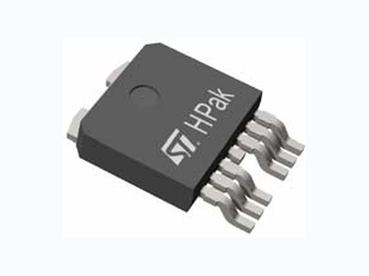
Datasheet-L5300AH7-Automotive 5 V low drop voltage regulator
Document overview
- Manufacturer or author: STMICROELECTRONICS
- PDF pages: 24
Technical content
Datasheet sections
- 1 Block diagram and pins descripti on
- 2 Electrical specifications
- 2.1 Absolute maximum ratings
- 2.2 Thermal data
- 2.3 Electrical characteristics
- 2.4 Electrical characteristics curves
- 3 Application information
- 3.1 Voltage regulator
- 3.2 Reset
- 3.3 Enable
- 4 Package and PC board thermal da ta
- 4.1 HPAK thermal data
- 5 Package and packing information
- 5.1 ECOPACK ®
- 5.2 HPAK mechanical data
- 6 Revision history
Features
AEC-Q100 qualified Operating DC supply voltage range 5.6 V to 40 V Low dropout voltage 300 mA current capability Low quiescent current Very low consumption mode Precision output voltage 5 V +/-2% Reset circuit sensing the output voltage Programmable reset pulse delay with external capacitor Thermal shutdown and short circuit protection Wide temperature range (Tj = -40°C to 150°C) Enable input for enabling / disabling the voltage regulator
Description
L5300AH7 is a low dropout linear regulator with microprocessor control functions such as power on reset, low voltage reset, ON/OFF control. In addition, only low value ceramic capacitor is required for stability (above or equal 220 nF). Typical quiescent current is 60 µA at output current equal to 0 and enable high. It drops to µA in “not enabled” mode. On chip trimming results in high output voltage accuracy (+/-2%). Accuracy is kept over wide temperature range, line and load variation. The maximum input voltage is 40 V. The max output current is internally limited. Internal temperature protection disables the voltage regulator output. Max DC supply voltage V s 40 V Max output voltage tolerance V0 +/-2 % Max dropout voltage V dp 500 mV Output current I 0 300 mA Quiescent current I qn 5 µA(1) 55 µA(2) 1. Typical value with regulator disabled 2. Typical value with regulator enabled HPAK GAPGCFT00135 Table 1. Device summary
1 Block diagram and pins description
Figure 1. Block diagram
Table 2. Pins description 1V S Supply voltage, block directly to GND on the IC with a capacitor. ground to adjust the reset delay time. Keep open if not needed. 6V os Output voltage sensing: this pin must be connected to Vo. (220 nF for regulator stability).
2 Electrical specifications
2.1 Absolute maximum ratings
extended periods may affect device reliability.
2.2 Thermal data
Table 3. Absolute maximum ratings Table 4. Thermal data
- The values quoted are for PCB 77 mm x 86 mm x 1.6 mm, FR4, double layer with thermal vias (one copper
heatsink layer, thickness 0.070 mm, area 8 cm2).
2.3 Electrical characteristics
Table 5. General
- Measured output current when the output voltage has dropped 100 mV from its nominal value obtained at
- V S - Vo measured dropout when the output voltage has dropped 100 mV from its nominal value obtained at
Table 6. Reset Table 7. Enable
2.4 Electrical char acteristics curves
Figure 3. Output voltage vs Tj Figure 4. Output voltage vs VS Figure 5. Output voltage vs VEn Figure 6. Drop voltage vs output current
Application information L5300AH7 14/24 DS6143 Rev 13
3 Application information
3.1 Voltage regulator
The voltage regulator uses a P-channel MOS transistor as a regulating element. With this structure a very low dropout voltage at current up to 300 mA is obtained. The output voltage is regulated up to input supply voltage of 40 V. The high-precision of the output voltage (+/-2%) is obtained with a pre-trimmed reference voltage. The voltage regulator automatically adapts its own quiescent current to the output current level. In light load conditions the quiescent current goes down to 55 µA only (low consumption mode). This procedure features a certain hysteresis on the output current (see Figure 8). Short-circuit protection to GND and a thermal shutdown are provided. Figure 21.Application schematic The input capacitor C1 100 µF is necessary as backup supply for negative pulses which may occur on the line. The second input capacitor C2 220 nF is needed when the C1 is too distant from the VS pin and it compensates smooth line disturbances. The C0 ceramic capacitor, connected to the output pin, is for bypassing to GND the high-frequency noise and it guarantees stability even during sudden line and load variations. Suggested value is C0 = 220 nF with ESR 100 m. Stability region is reported in Figure 22. 9%$77 /$+ 567 9FU *1' & & *$3*&)7
Application information L5300AH7 16/24 DS6143 Rev 13
3.2 Reset
The reset circuit monitors the output voltage Vo. If the output voltage becomes lower than Vo_th then Res goes low with a delay time (trr). When the output voltage becomes higher than Vo_th then Res goes high with a delay time Trd. This delay is obtained by 512 periods of oscillator. The oscillator period is given by: Equation 1 Tosc = [(VRhth-VRlth) x Ctr] / Icr + [(VRhth-VRlth) x Ctr] / Idr and reset pulse delay Trd is given by: Equation 2 trd = 32 x Tosc Where: Icr = 20 µA is an internally generated charge current, Idr = 20 µA is an internally generated discharge current, VRhth = 2.5V (typ) and VRlth = 0.95V (typ) are two voltage thresholds, Ctr is an external capacitor put between Vcr pin and GND. Figure 24.Reset time diagram
3.3 Enable
L5300AH7 is also provided by an enable input, a high signal switches the regulator ON. In standby mode the output is disabled and the current consumption of the device (quiescent current) is less than 10 µA. 9FU 5HV WUU WUU WUG 7RVF 9RXWBWO 9UKWK 9UOWK *$3*&)7
4 Package and PC board thermal data
4.1 HPAK thermal data
Figure 25.PC board Figure 26.Rthj-amb vs PCB copper area in open box free air condition *$3*&)7 Note: Layout condition of Rth and Zth measurements (Board finish thickness 1.6 mm +/- 10 %; Board double layer; Board dimension 78 mm x 86 mm; Board Material FR4; Cu thickness 0.070 mm (front and back side); Thermal vias separation 1.2 mm; Thermal 02468 1 0 RTHjamb RTHjamb GAPGCFT00131
Table 8. Thermal parameter
Package and packing information L5300AH7 20/24 DS6143 Rev 13
5 Package and packing information
5.1 ECOPACK ®
In order to meet environmental requirements, ST offers these devices in different grades of ECOPACK® packages, depending on their level of environmental compliance. ECOPACK® specifications, grade definitions and product status are available at: www.st.com. ECOPACK® is an ST trademark.
5.2 HPAK mechanical data
Figure 29.HPAK dimension GAPGCFT00134
Table 9. HPAK mechanical data
6 Revision history
Table 10. Document revision history 09-Aug-2007 1 Initial release.
- quiescent current with regulator disabled changed from 10 to 5 µA.
- quiescent current with regulator enabled changed from 60 to 55 µA.
Changed status from target specification to preliminary data. Added Section 2.4: Electrical characteristics curves.
26-Jan-2012 10 Updated Figure 22: Stability region on page 15. 07-Feb-2012 11 Modified Figure 22: Stability region on page 15. 13-Sep-2013 12 Updated disclaimer. 21-Sep-2018 13 Updated template. Table 10. Document revision history (continued)