
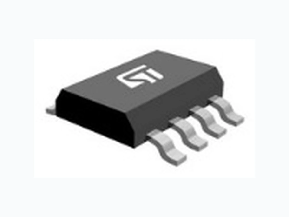
L5050 STMICROELECTRONICS
Document overview
- Manufacturer or author: STMICROELECTRONICS
- PDF pages: 25
Technical content
Datasheet sections
- 1 Block diagram and pins description
- 2 Electrical specifications
- 2.1 Absolute maximum ratings
- 2.2 Electrical characteristics
- 2.3 Electrical characteristics curves
- 3 Protection features
- 3.1 Voltage regulator
- 3.2 Enable
- 4 Package and PCB thermal data
- 5 Package information
- 5.1 SO-8 package information
- 5.2 SO-8 packaging information
Features
VS Max DC supply voltage 40 V ΔVO Max output voltage tolerance ± 2% Vdp Max dropout voltage 500 mV IO Output current 50 mA (1) 2x50 mA (2) Iqn Quiescent current 50 µA (3) 1. For L5050S - single output. Up to 100 mA as pulsed current 2. For L5050SD - dual output. Up to 2x100 mA as pulsed current. 3. Typical value valid for each single output with En = LOW.
- AEC-Q100 qualified
- Operating DC supply voltage range 5.6 V to 40 V
- Low dropout voltage
- Low quiescent current consumption
- Up to 100 mA and 2x100 mA as pulsed current
- Precision output voltage 5 V ± 2%
- Dual electrically isolated voltage regulators (only for L5050SD)
- Enable input for enabling/disabling the voltage regulator
- Thermal shutdown and short circuit protection
- Wide temperature range (T J = -40 °C to 150 °C)
Description
L5050 is a 5 V low dropout linear voltage regulator suitable for automotive applications, available in single (L5050S) or dual isolated (L5050SD) linear output voltage in a SO-8 package. The LDO delivers up to 50 mA (2x50 mA for the dual version) of DC load current and consumes as low as 5 μA (per each output in L5050SD) of quiescent current with device disabled. High output voltage accuracy (± 2%) is kept over wide temperature range, line and load variation. The L5050S is able to deliver up to 100 mA (as pulsed current) and L5050SD up to 2x100 mA (as pulsed current); duration of current is linked to thermal settings (such as PCB type, ambient temperature). Enable features (two enables for the dual version) allow enabling or disabling each output. The maximum input voltage is 40 V. The regulator output current is internally limited and the device is protected against short circuit, overload and over temperature conditions. In addition, only low value ceramic capacitor on output is required for stability. Product status link L5050 Product summary Order code L5050STR L5050SDTR Package SO-8 Packing Tape and reel Single and dual isolated 5 V low drop linear voltage regulators for automotive application L5050 Datasheet DS13704 - Rev 3 - July 2022 For further information contact your local STMicroelectronics sales office.
1 Block diagram and pins description
Figure 1. Functional block diagram - L5050S Table 1. L5050S pins description VS 6 Supply voltage, block directly to GND on the IC with a capacitor.
Figure 2. Functional block diagram - L5050SD Table 2. L5050SD pins description
- high signal to switch the regulator on VS1 7 Supply voltage 1, block directly to GND1 on the IC with a capacitor. En1 8 Enable pin for regulator 1:
- high signal to switch the regulator on L5050 Block diagram and pins description DS13704 - Rev 3 page 3/25
Figure 3. Pins configuration
2 Electrical specifications
2.1 Absolute maximum ratings
program and other relevant quality documents. Table 3. Absolute maximum ratings
- ±500 V for En1 and En2 (only for L5050SD).
Table 4. Thermal data
- PCB: single layer; FR4 area = 77 mm x 86 mm; PCB thickness = 1.6 mm; Cu thickness = 70 µm (front side), Cu area = 2
2.2 Electrical characteristics
Values specified in this section are for VS = 5.6 V to 31 V, TJ = - 40 °C to +150 °C, unless otherwise stated. Table 5. General
- Those parameters are achieved by characterization on a small sample size from typical devices under typical conditions.
- Up to 100 mA as pulsed current.
- Measured output current when the output voltage has dropped 200 mV from its nominal value obtained at Vs = 10.5 V and
- Thermal protection is guaranteed by design and characterization.
Electrical characteristics
Table 6. Enable
2.3 Electrical characteristics curves
Figure 4. Output voltage vs TJ Figure 5. Output voltage vs Vs Figure 6. Output voltage vs Ven Figure 7. Drop voltage vs output current Figure 8. Current consumption vs output current Figure 9. Current consumption vs output current (at light
3 Protection features
3.1 Voltage regulator
Figure 9. Current consumption vs output current (at light load condition)). Short-circuit protection to GND and a thermal shutdown are provided. Figure 19. Application schematic - L5050S
C2 ≥ 220 nF is needed when the C1 is too distant from the VS pin and it compensates smooth line disturbances. mΩ. Stability region is reported in the figure below. Figure 22. Stability region Figure 23. Maximum load variation response
3.2 Enable
L5050 features enable input (two enable input pins for the L5050SD, one for each voltage regulator). (quiescent current) is typically 5 μA.
4 Package and PCB thermal data
Figure 24. SO-8 PC board for L5050S PCB thickness = 1.6 mm; Cu thickness = 70 μm (front side), Cu area = 2 cm^2 for L5050S (picture on the right)). Figure 25. SO-8 PC board for L5050SD
Table 7. L5050S SO-8 thermal parameter Table 8. L5050SD SO-8 thermal parameter
5 Package information
In order to meet environmental requirements, ST offers these devices in different grades of ECOPACK packages, depending on their level of environmental compliance. ECOPACK specifications, grade definitions and product status are available at: www.st.com. ECOPACK is an ST trademark.
5.1 SO-8 package information
Figure 31. SO-8 package outline
Package information
DS13704 - Rev 3 page 18/25
Table 9. SO-8 mechanical data Figure 32. SO-8 recommended footprint (dimensions are in mm)
5.2 SO-8 packaging information
Figure 33. SO-8 tape and reel shipment (suffix “TR”)
Revision history
Table 10. Document revision history 19-Apr-2021 1 Initial release.
- Section Features;
- Section Description;
- Section 4 Package and PCB thermal data;
- Table 4. Thermal data;
- Table 5. General;
- Figure 28. SO-8 thermal impedance junction ambient single pulse (one channel on for L5050SD). Minor text changes. 26-Jul-2022 3 Updated Table 5. General. Minor text changes in:
- Section Description;
- Section 3.1 Voltage regulator. L5050 DS13704 - Rev 3 page 21/25
IMPORTANT NOTICE – READ CAREFULLY STMicroelectronics NV and its subsidiaries (“ST”) reserve the right to make changes, corrections, enhancements, modifications, and improvements to ST products and/or to this document at any time without notice. Purchasers should obtain the latest relevant information on ST products before placing orders. ST products are sold pursuant to ST’s terms and conditions of sale in place at the time of order acknowledgment. Purchasers are solely responsible for the choice, selection, and use of ST products and ST assumes no liability for application assistance or the design of purchasers’ products. No license, express or implied, to any intellectual property right is granted by ST herein. Resale of ST products with provisions different from the information set forth herein shall void any warranty granted by ST for such product. ST and the ST logo are trademarks of ST. For additional information about ST trademarks, refer to www.st.com/trademarks. All other product or service names are the property of their respective owners. Information in this document supersedes and replaces information previously supplied in any prior versions of this document. © 2022 STMicroelectronics – All rights reserved L5050 DS13704 - Rev 3 page 25/25