


 Download PDF
KST-312 KODENSHI
Document overview
- PDF pages: 2
Technical content
Page 1
Photo transistors
K O D E N S H I
K S T - 3 1 2
The KST- 312 is a high- sensitivity Silicon phototransistor with two- phaseoutput. This phototransistor is compact , and the best for the m o u s e .
F E A T U R E S
- Visible ray cut off mold type
- Bult- in 2ch phototransistors
A P P L I C A T I O N S
- Optical mouses
- E n c o d e r s
MAXIMUM RATINGS
| It e m | Sy m b o l | Ra t i n g | Un i t |
| C- E voltage | VCE O | 3 0 | V |
| E- C voltage | VEC O | 5 | V |
| Collector current | IC | - | m A |
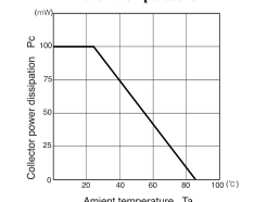
| Collector power dissipation | P C | 1 0 0 | m W |
| Operating temp. | T o p r . | - 2 5 ~ + 8 5 | ℃ |
| Storage temp. | T s t g . | - 3 0 ~ + 8 5 | ℃ |
| Soldering temp. *1 | T s o l . | 2 6 0 | ℃ |
\*1. For MAX.5 seconds at the position of 2 mm from the package
ELECTRO-OPTICAL CHARACTERISTICS
D I M E N S I O N S
(Unit : mm)
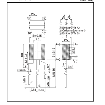
( T a = 2 5℃)
( T a = 2 5℃)
| It e m | Sy m b o l | Co n d i t i o n s | Mi n . T | y p . | Ma x . | Un i t . | |
| Collector dark current | ICE O | VCE O = 1 0 V | 1 0 0 | n A | |||
| Light current | IL | VCE = 5 V , 1 m W / c m2 | 1 6 0 | 9 6 0 | μA | ||
| C- E saturation voltage | VCE ( s a t ) | IC= 1 0 0μA | 0 | . 1 | 0 . 4 | V | |
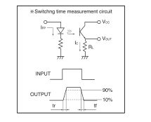
| Switching speeds | Rise time | t r | VCC = 5V, IC= 1 m A , R L= 1 KΩ | 1 5 | μs e c . | ||
| Fall time | t f | 1 8 | μs e c . | ||||
| Spectral sensitivity | λ | 8 8 0∼1 0 5 0 | n m | ||||
| Peak wavelength | λ p | 8 | 8 0 | n m | |||
| Half angle | △θ | ± | 6 0 | d e g . | |||
- 1-
Page 2
Photo transistors
K S T - 3 1 2
Collector current Vs.
Collector current Vs.
Dark current Vs.
Collector - Emitter voltage
Illuminance
Ambient temperature
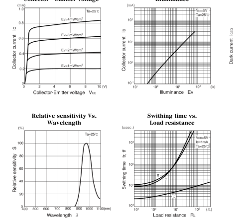
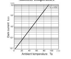
Radiant Pattern
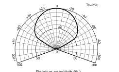
Collector power dissipation Vs. Ambient temperature
- 2-