


 Download PDF
KPI-511 KODENSHI
Document overview
- PDF pages: 2
Technical content
Page 1
Photointerrupter(Transmissive)
KPI-511
DESCRIPTION
DIMENSIONS
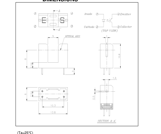
The photointerrupter high-performance standard type KPI-511 combines a high-output GaAs IRED with a high sensitivity phototransistor.
FEATURES
- PWB direct mount type
- GAP : 5.0mm
APPLICATIONS
- Printers
- Copiers
- A T M
- Ticket Vending Machines
ABSOLUTE MAXIMUM RATINGS
| Parameter | Symbol | Rating | Unit | |
|---|---|---|---|---|
| Input | Forward Current | I F | 60 | mA |
| Pulse Forward Current *1 | I FP | 1 | A | |
| Reverse Voltage | V R | 5 | V | |
| Power Dissipation | P D | 100 | mW | |
| Output | Collector Emitter Voltage | V CEO | 30 | V |
| Emitter Collector Voltage | V ECO | 5 | V | |
| Collector Current | I C | 40 | mA | |
| Collector Power Dissipation | P C | 100 | mW | |
| Operating Temperature *2 | T OPR | -25 ~ +85 | ℃ | |
| Storage Temperature *2 | T STG | -40 ~ +85 | ℃ | |
| Soldering Temperature *3 | T SOL | 260 | ℃ | |
\*1. Pulse width : tw≤100µsec.period : T=10msec \*2. No icebound or dew \*3. For MAX. 5 seconds at the position of 1mm from the package
ELECTRO-OPTICAL CHARACTERISTICS
(Ta=25℃)
| Parameter | Symbol | Conditions | MIN. | TYP. | MAX. | Unit | ||
|---|---|---|---|---|---|---|---|---|
| Input | Forward Voltage | V F | I =20mA F | - | 1.2 | 1.7 | V | |
| Reverse Current | I R | V =5V R | - | - | 10 | µA | ||
| Capacitance | C T | f=1KHz | - | 25 | - | F P | ||
| Peak Wavelength | ? P | - | - | 940 | - | nm | ||
| Output | Dark Current | I CEO | V =10V, 0 Lux CE | - | - | 10 | µA | |
| Coupled | Light Current | I L | V =5V, I = 20mA (Non-shading) CE F | 0.5 | - | 15 | mA | |
| Collector Emitter Saturation Voltage | V CE(SAT) | I =20mA, I =0.1mA F C | - | - | 0.4 | V | ||
| Response Time | Rise Time | tr | V =5V, I =2mA, CC C R=100Ω L | - | 5 | - | µs | |
| Fall Time | tf | - | 5 | - | µs | |||
1/2
Page 2
Photointerrupter(Transmissive)
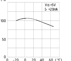
Collector power dissipation Vs. Ambient temparature ( ㎽)
( ㎃) KPI-511
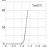
Forward current Vs.
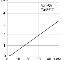
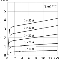
Light current Vs.
Forward voltage
Forward current ( ㎃)
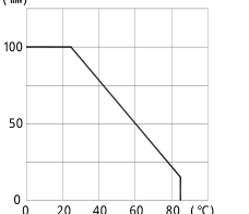
Ambient temperature(Ta) Ambient temperature(Ta)
Light current Vs. Collentor-Emitter voltage
(%)
( ㎃)
For ward vol tage( V )
For ward Current( I ) Forward Current( IF )
Forward voltage( VF)
F
F
Relative light current Vs.
Dark current Vs.
Ambient temperature
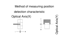
Ambient temperature Y
(%) X
Col l ector- Emi tt er Vol tage( V ) Collector-Emitter Voltage( VCE )
CE
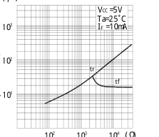
Switching time Vs.
V =5V
V =5V
CC
CC C Ta=25˚
C Ta=25˚
I =10mA
I =10mA
F
F
100
50
0 - 2 0 +2 - 2 0 +2 ( mm)
Ambi ent t emper ature( Ta)
Movi ng di stance(L)
Ambient temperature( Ta )
Moving distance( L )
Response ti me measurement ci rcui t Response time measurement circuit
Load resistance
V
Input
CC
( ㎲)
V OUT I C R L
Input
90%
Out put
10% t d t r t f
10 10 10
Load Resistance( RL ) Road Resi stance( R )
L
2/2