
 Download PDF
KDT-6315A KODENSHI
Document overview
- PDF pages: 2
Technical content
Page 1
AUK CORP.
Photo Transistor
KDT-6315A
Description
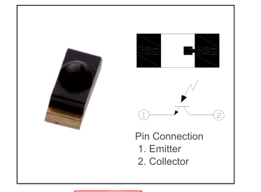
The KDT-6315A is a high-sensitivity & surface mount type silicon phototransistor. It’s ideal for various kinds of optical transistor such as touch panels for C/D, ATM, Car navigation system and even AV Instrument and various types of disk driver.
Features
Compact and thin package SMD type Reflow soldering RoHS & High reliability package
Applications
Touch screen for ATM Touch screen for Car navigation system Touch screen for FA equipment AV instrument Various types of disk driver
Absolute Maximum Ratings
[TA = 25 ]
| Parameter | Symbol | Min. | Max. | Max. |
|---|---|---|---|---|
| Collector-Emitter Voltage | V CEO | - | 35 | V |
| Emitter-Collector Voltage | V ECO | - | 6 | V |
| Collector Current | I C | - | 20 | ㎃ |
| Collector Power Dissipation | P C | - | 75 | ㎽ |
| Operating Temperature | Topr. | -20 | 85 | |
| Storage Temperature | Tstg. | -30 | 85 | |
| Soldering Temperature*1 | Tsol | - | 260 |
\*1 : MAX 10s
The contents of this data sheet are subject to change without advance notice for the purpose of improvement. When using this product, would you please refer to the latest specifications.
Page 2
KDT-6315A
Electrical Characteristics
[TA = 25 ]
| Parameter | Symbol | Conditions | Min. | Typ. | Max. | Unit |
|---|---|---|---|---|---|---|
| Dark Current | I CEO | Ev=0, VCE=20V | - | 1.0 | 100 | ㎁ |
| Collector Current | I C | Ev=1000lx, VCE=5V | 4.0 | 6.0 | - | ㎃ |
| Collector-Emitter Saturation Voltage | V CE(SAT) | Ev=1000lx, IC=0.8mA | - | 0.15 | 0.4 | V |
| Spectral Sensitivity | λ | - | 700 | - | 1050 | ㎚ |
| Peak Sensitivity Wavelength | λ P | - | - | 880 | - | ㎚ |
| Collector-Emitter Breakdown Voltage | BVCEO | Ev=0, ICE=0.1mA | 35 | 90 | - | V |
| Emitter-Collector Breakdown Voltage | BVECO | Ev=0, IEC=0.01mA | 6 | 7.5 | - | V |
| Half Angle | ∆θ | - | - | ±15 | - | deg |
Ordering Information
| Part Number | Packaging Type | Quantity |
|---|---|---|
| KDT-6315A | Tape and Reel | 4,000 |
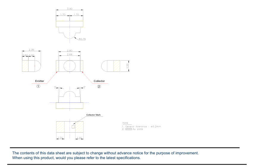
Package Outline Dimensions
(Unit : mm)