


 Download PDF
K5610 KODENSHI
Document overview
- PDF pages: 3
Technical content
Page 1
Photocoupler
K5610 • K5611
These Photocouplers consist of a Gallium Arsenide Infrared Emitting
DIMENSION (Unit : mm)
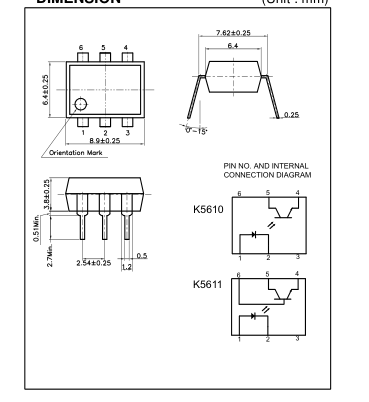
Diode and a Silicon NPN Phototransistor in a 6-pin package.
FEATURES
- TTL Compatible Output
- Collector-Emitter Voltage : Min.70V
- Current Transfer Ratio : Typ.50% (at IF=5mA, VCE=5V)
- Electrical Isolation Voltage : AC5000Vrms
- UL Recognized File No. E107486
APPLICATIONS
- Interface between two circuits of different potential
- Vending Machine, Copiers
- Measuring Instrument
- Home Appliances
MAXIMUM RATINGS
(Ta=25℃ )
| Parameter | Symbol | Rating | Unit | |
|---|---|---|---|---|
| Input | Forward Current | IF | 50 | mA |
| Reverse Voltage | VR | 5 | V | |
| *1 Peak Forward Current | IFP | 1 | A | |
| Power Dissipation | PD | 70 | mW | |
| Output | Collector-Emitter Breakdown Voltage | BVCEO | 70 | V |
| Emitter-Collector Breakdown Voltage | BVECO | 7 | V | |
| Collector-Base Breakdown Voltage** | BVCBO | 80 | V | |
| Collector Current | IC | 50 | mA | |
| Collector Power Dissipation | PC | 150 | mW | |
| *2 Input to Output Isolation Voltage | Viso | AC5000 | Vrms | |
| Storage Temperature | Tstg | -55~+125 | ℃ | |
| Operating Temperature | Topr | -30~+100 | ℃ | |
| *3 Lead Soldering Temperature | Tsol | 260 | ℃ | |
| Total Power Dissipation | Ptot | 200 | mW | |
\*\* Except for K5610 \*1. Input current with 100㎲ pulse width, 1% duty cycle \*2. Measured at RH=40~60% for 1min \*3. 1/16 inch form case for 10sec
1/3
Page 2
Photocoupler
K5610 • K5611
ELECTRO-OPTICAL CHARACTERISTICS
(Ta=25℃ , unless otherwise noted)
| Parameter | Symbol | Condition | Min. | Typ. | Max. | Unit. | |
|---|---|---|---|---|---|---|---|
| Input | Forward Voltage | VF | IF=10mA | - | 1.15 | 1.30 | V |
| Reverse Current | I R | VR=5V | - | - | 10 | ㎂ | |
| Capacitance | CT | V=0, f=1MHz | - | 30 | - | pF | |
| Output | Collector-Emitter Breakdown Voltage | BVCEO | IC=1mA | 70 | - | - | V |
| Emitter-Collector Breakdown Voltage | BVECO | IE=0.1mA | 7 | - | - | V | |
| Collector-Base Breakdown Voltage ** | BVCBO | I =0.1mA C | 80 | - | - | V | |
| Collector Dark Current | ICEO | IF=0, VCE=24V | - | - | 100 | nA | |
| Capacitance | CCE | VCE=0, f=1MHz | - | 10 | - | pF | |
| Coupled | *4 Current Transfer Ratio | CTR | IF=5mA, VCE=5V | 50 | - | 600 | % |
| Collector-Emitter Saturation Voltage | VCE(SAT) | IF=5mA, IC=1mA | - | - | 0.3 | V | |
| Input-Output Capacitance | CIO | V=0, f=1MHz | - | 1 | - | pF | |
| Input-Output Isolation Resistance | RIO | RH=40~60%, V=500V | - | 1011 | - | Ω | |
| Rise Time | tr | VCE=10V, RL=100Ω IC=2mA | - | 3 | - | ㎲ | |
| Fall Time | tf | - | 3 | - | ㎲ | ||
\*\* Except for K5610 \*4. CTR=(IC/IF) X 100 (%)
2/3
Page 3
Photocoupler
K5610 • K5611
Forward Current vs.
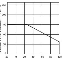
Collector Power Dissipation vs.
Ambient Temperature
Ambient Temperature
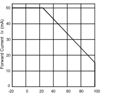
Ambient Temperature Ta (℃ )
Ambient Temperature Ta (℃ )
Collector Current vs.
Dark Current vs.
Collector-Emitter Voltage
Ambient Temperature
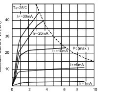
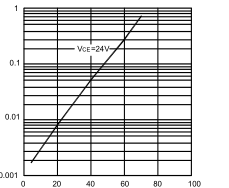
Collector-Emitter Voltage VCE (V)
Ambient Temperature Ta (℃)
Collector Current vs.
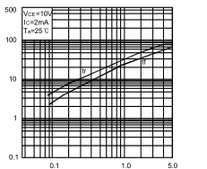
Response Time vs.
Forward Current
Load Resistance
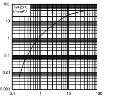
Forward Current IF (mA)
Load Resistance RL (㏀)
3/3
3/3
Forward Current vs. Forward Voltage
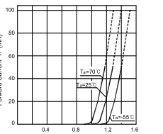
Forward Voltage VF (V)
Collector Current vs. Ambient Temperature
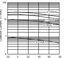
Ambient Temperature Ta (℃ )
Switching Time Test Circuit
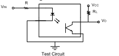
Input
Output 10%
90% tr tf
Waveform