


 Download PDF
IP3337CX18 NXP
Document overview
- PDF pages: 13
Technical content
Page 1
7-channel integrated LC-filter network with ESD input
protection to IEC 61000-4-2 level 4
1. Product profile
1.1 General description
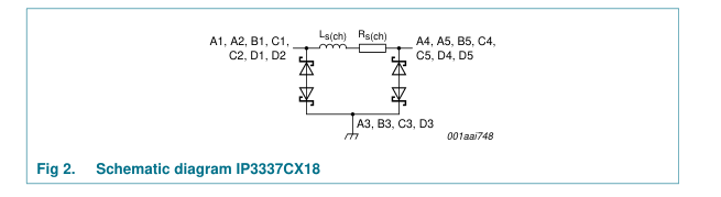
The IP3337CX18 is a 7-channel1 LC low-pass filter network designed to filter undesired RF signals in the 800 MHz to 3000 MHz frequency band. In addition, the IP3337CX18 incorporates diodes which protect downstream components from ElectroStatic Discharge (ESD) voltages as high as 15 kV.
The IP3337CX18 is fabricated using monolithic silicon technology and integrates 7 inductors, 14 back-to-back diodes in a single Wafer-Level Chip-Scale Package (WLCSP) measuring 2.06 mm by 1.66 mm (typical). These features make the IP3337CX18 ideal for use in applications requiring the utmost in miniaturization such as mobile phone handsets, cordless telephones and personal digital devices.
1.2 Features
I Pb-free, RoHS compliant and halogen free package; Dark Green compliant I Integrated 7-channel π-type LC-filter network with 60 nH channel inductance I 125 Ω series resistance, 25 pF (typical) capacitance per line I Integrated ESD protection withstanding ±15 kV contact discharge, far exceeding IEC 61000-4-2, level 4 I WLCSP with 0.4 mm pitch
1.3 Applications
I Cellular and PCS mobile handsets I Cordless telephones I Wireless data (WAN/LAN) systems and PDAs
- Also available as a 10-channel device (IP3338CX24).

Page 2
2. Pinning information
2.1 Pinning
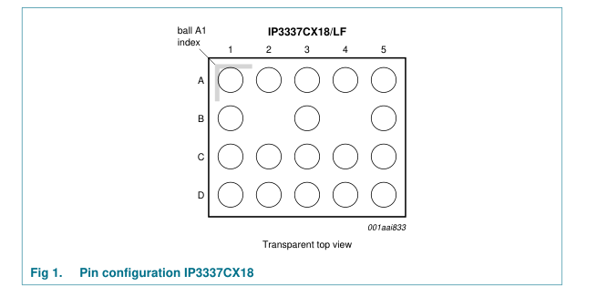
Table 1. Pinning Pin A2 and A5 A1 and A4 B1 and B5 C2 and C5 C1 and C4 D2 and D5 D1 and D4 A3, B3, C3, D3 B2 and B4
3. Ordering information
Table 2. Ordering information
Description
filter channel 1 filter channel 2 filter channel 3 filter channel 4 filter channel 5 filter channel 6 filter channel 7 ground no balls
| Type number | Package | ||
|---|---|---|---|
| Name | Description | Version | |
WLCSP18 wafer level chip-size package; 18 bumps; 2.06 × 1.66 × 0.61 mm
IP3337CX18/LF
IP3337CX18/LF
2 of 13
Page 3
4. Functional diagram
5. Limiting values
Table 3. Limiting values In accordance with the Absolute Maximum Rating System (IEC 60134). Symbol
Parameter input voltage
VI
electrostatic discharge voltage
VESD
channel current (DC)
Ich
peak channel current
Ich(M)
channel power dissipation
Pch
total power dissipation
Ptot
storage temperature
Tstg
peak reflow temperature
Treflow(peak)
ambient temperature
Tamb
Conditions
Min Max Unit −4.0 +4.0 V
all pins to ground
[1] −15 +15 kV
contact discharge
[1] −15 +15 kV
air discharge IEC 61000-4-2, level 4; all pins to ground contact discharge
−8 +8 kV
air discharge
−15 +15 kV
Tamb = 70 °C
- 10 mA
Tamb = 70 °C; 60 s
- 50 mA
continuous power;
- 10 mW
Tamb = 70 °C Tamb = 70 °C
- 70 mW
−55 +150 °C
10 s maximum
- 260 °C −35 +85 °C
[1] Device tested with 1000 pulses of ±15 kV contact discharges, according to the IEC 61000-4-2 model, which far exceeds IEC 61000-4-2, level 4 (8 kV contact discharge).
3 of 13
Page 4
6. Characteristics
Table 4. Channel characteristics Tamb = 25 °C; unless otherwise specified. Symbol Parameter channel series resistance Rs(ch) channel capacitance Cch channel series inductance Ls(ch) breakdown voltage VBR
reverse leakage current ILR
[1] Guaranteed by design.
Table 5. Frequency characteristics Tamb = 25 °C; unless otherwise specified. Symbol Parameter insertion loss αil
cut-off frequency f−3dB
crosstalk attenuation αct
7. Application information
7.1 Insertion loss
Conditions
Min Typ Max Unit
f = 0 Hz (DC)
100 125 150 Ω 25 30[1] pF
Vbias(DC) = 0 V; f = 1 MHz
- [1] - 60 -
nH
Itest = 1 mA
6 - 10 V
Itest = −1 mA
−10 -
−6 V
per channel; VI = 3.0 V
- - 100 nA
Conditions
Min Typ Max Unit
Rgen = 50 Ω; RL = 50 Ω 800 MHz < f < 1 GHz
38 40 -
dB
1 GHz < f < 3 GHz
35 40 -
dB
at 0 Hz; Rgen = 50 Ω;
6 7 10 dB
RL = 50 Ω; Vbias(DC) = 0 V measured relative to
150 180 -
MHz
insertion loss at DC; Rgen = 50 Ω; RL = 50 Ω 800 MHz < f < 3 GHz;
35 40 -
dB
Rgen = 50 Ω; RL = 50 Ω
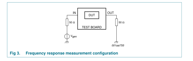
The setup for measuring insertion loss in a 50 Ω system is shown in Figure 3.
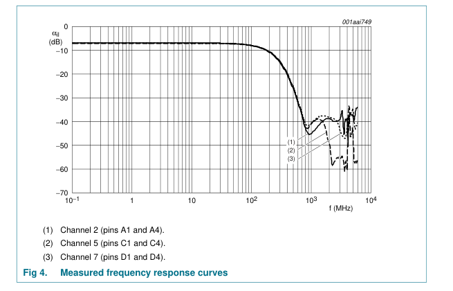
The measured frequency response curves for all channels are shown in Figure 4.
4 of 13
Page 5
7.2 Crosstalk
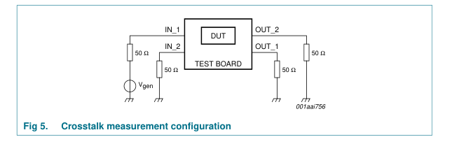
The setup for measuring crosstalk in a 50 Ω system is shown in Figure 5.
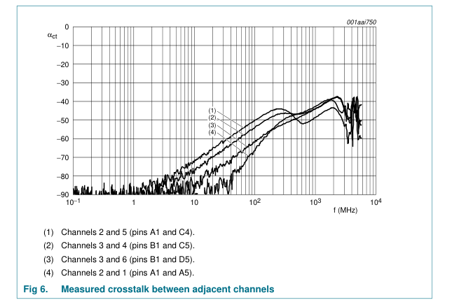
The crosstalk between adjacent channels within the IP3337CX18 for different channel pairs measured in a 50 Ω NetWork Analyzer (NWA) system, is shown in Figure 6. In all cases, all unused connections are terminated with 50 Ω to ground.
5 of 13
Page 6
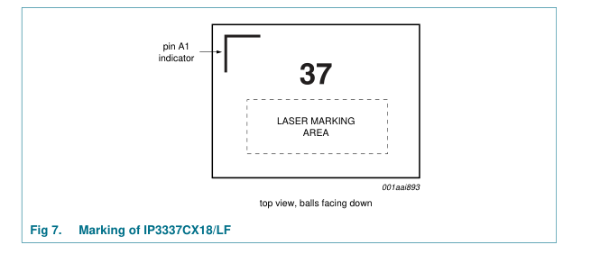
8. Marking
6 of 13
Page 7
9. Package outline
WLCSP18: wafer level chip-size package; 18 bumps; 2.06 x 1.66 x 0.61 mm
IP3337CX18/LF
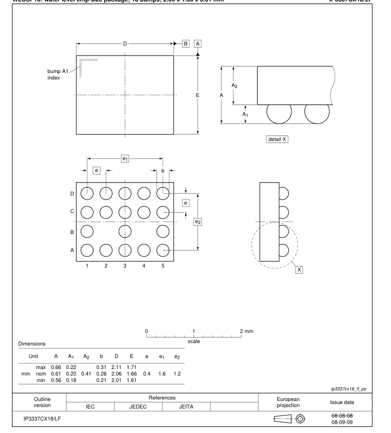
Fig 8. Package outline IP3337CX18/LF (WLCSP18)
7 of 13
Page 8
10. Packing information
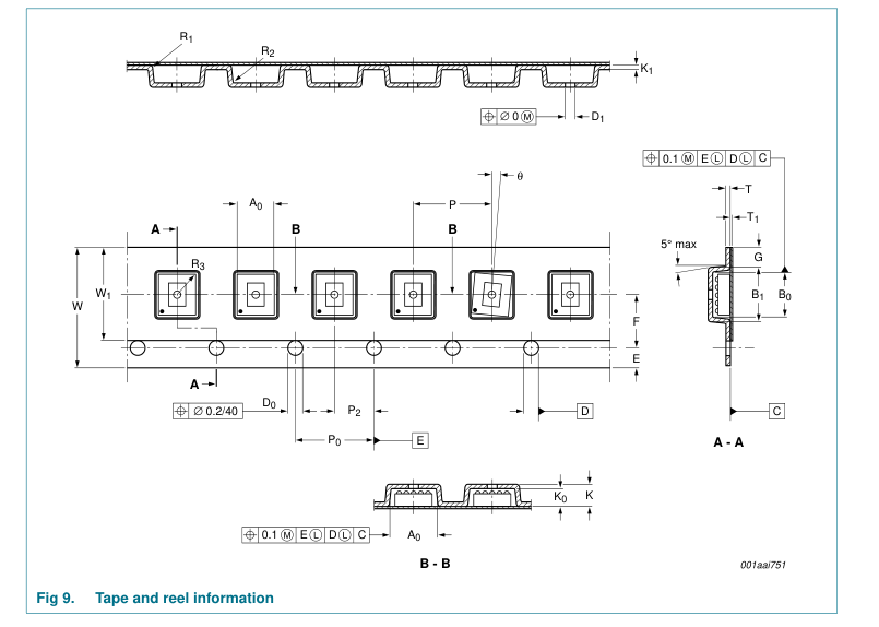
Table 6. Tape dimensions Item
Overall dimensions
Sprocket holes[1]
Distance between center lines
| Specification (mm) | |
| Dimension | Tolerance |
Parameter
Symbol
tape width
W 8.00
±0.3
thickness
K 1.20
maximum
distance
G 0.75
minimum
outside width
B1 3.70
maximum
diameter
D0 1.50
+0.1/−0.0
distance
E 1.75
±0.1
pitch
P0 4.00
±0.1
length direction
P2 2.00
±0.05
width direction
F 3.50
±0.05
8 of 13
Page 9
Table 6. Tape dimensions …continued
| Item Parameter Symbol | Specification (mm) | |
|---|---|---|
| Dimension | Tolerance | |
Compartments
Device Carrier tape anti-static[2] Cover tape[3]
Bending pad
length
A0 1.90
±0.05
width
B 0 2.35
±0.05
depth
K0 0.80
±0.05
hole diameter
D1 0.50
±0.1
pitch
P 4.00
±0.1
radius
R1 0.40
maximum
radius
R2 0.30
maximum
radius
R3 0.30
typical
depth
K1 0...0.25
−0.1
rotation
±10° θ
film thickness
T 0.25
±0.07
width
W1 5.75
max
film thickness
T1 0.1
max
in winding
R 30
min
direction
[1] Cumulative pitch error: ±0.2 mm per 10 pitches. [2] Carbon-loaded polystyrene 100 % recyclable. [3] The cover tape must not overlap the sprocket holes.
9 of 13
Page 10
11. Design and assembly recommendations
11.1 PCB design guidelines
For optimum performance it is recommended to use a Non-Solder Mask PCB Design (NSMD), also known as a copper-defined design, incorporating laser-drilled micro-vias connecting the ground pads to a buried ground-plane layer. This results in the lowest possible ground inductance and provides the best high frequency and ESD performance. For this case, refer to Table 7 for the recommended PCB design parameters.
Table 7. Recommended PCB design parameters Parameter PCB pad diameter Micro-via diameter Solder mask aperture diameter Copper thickness Copper finish PCB material
Value or Specification 200 µm 100 µm (0.004 inch) 337 µm 20 µm to 40 µm OSP FR4
11.2 PCB assembly guidelines for Pb-free soldering
Table 8. Assembly recommendations Parameter Solder screen aperture diameter Solder screen thickness Solder paste: Pb-free Solder/flux ratio Solder reflow profile
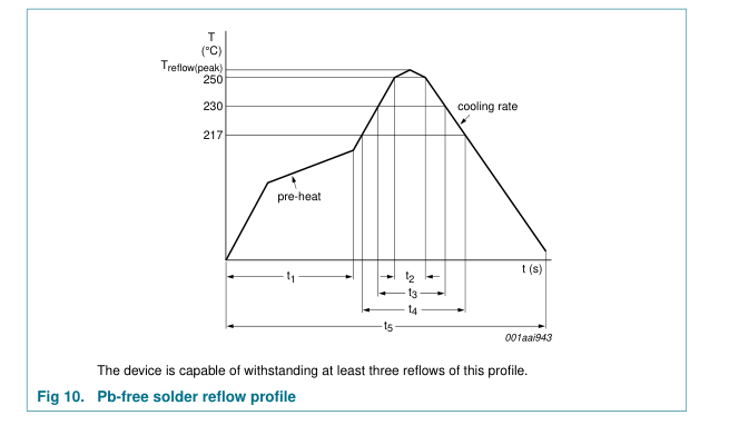
Value or Specification 330 µm 100 µm (0.004 inch) SnAg (3 % to 4 %) Cu (0.5 % to 0.9 %) 50/50 see Figure 10
10 of 13
Page 11
Table 9. Characteristics Symbol Parameter peak reflow temperature
Treflow(peak)
time 1
t1
time 2
t2
time 3
t3
time 4
t4
time 5 t5 dT/dt
rate of change of temperature
12. Abbreviations
Table 10. Abbreviations Acronym
Description
DUT
Device Under Test
Conditions
Min Typ Max Unit 230 -
255 °C
soak time
60 - 180 s
time during T ≥ 250 °C
- - 30 s
time during T ≥ 230 °C
10 - 50 s
time during T > 217 °C
30 - 150 s
- - 540 s
cooling rate
- - −6 °C/s
pre-heat
2.5 -
4.0 °C/s
ElectroMagnetic Interference
EMI ESD
ElectroStatic Discharge
FR4
Flame Retard 4
LAN
Local Area Network
NSMD
Non-Solder Mask Design Organic Solderability Preservative
OSP PCB
Printed-Circuit Board Personal Communication System
PCS PDA
Personal Digital Assistant
PSU
Power Supply Unit Restriction of Hazardous Substances
RoHS WAN
Wide Area Network Wafer-Level Chip-Scale Package
WLCSP
13. Revision history
Table 11. Revision history Document ID
Release date
Data sheet status
Change notice Supersedes
20081112
-
-
11 of 13
Page 12
14. Legal information
14.1 Data sheet status
Document status[1][2]
Product status[3]
Definition This document contains data from the objective specification for product development.
Objective [short] data sheet
Development
This document contains data from the preliminary specification.
Preliminary [short] data sheet Qualification
This document contains the product specification.
Product [short] data sheet
Production
[1] Please consult the most recently issued document before initiating or completing a design. [2] The term ‘short data sheet’ is explained in section “Definitions”. [3] The product status of device(s) described in this document may have changed since this document was published and may differ in case of multiple devices. The latest product status information is available on the Internet at URL http://www.nxp.com.
14.2 Definitions
Draft — The document is a draft version only. The content is still under internal review and subject to formal approval, which may result in modifications or additions. NXP Semiconductors does not give any representations or warranties as to the accuracy or completeness of information included herein and shall have no liability for the consequences of use of such information. Short data sheet — A short data sheet is an extract from a full data sheet with the same product type number(s) and title. A short data sheet is intended for quick reference only and should not be relied upon to contain detailed and full information. For detailed and full information see the relevant full data
sheet, which is available on request via the local NXP Semiconductors sales office. In case of any inconsistency or conflict with the short data sheet, the full data sheet shall prevail.
14.3 Disclaimers
General — Information in this document is believed to be accurate and reliable. However, NXP Semiconductors does not give any representations or warranties, expressed or implied, as to the accuracy or completeness of such information and shall have no liability for the consequences of use of such information. Right to make changes — NXP Semiconductors reserves the right to make changes to information published in this document, including without limitation specifications and product descriptions, at any time and without notice. This document supersedes and replaces all information supplied prior to the publication hereof. Suitability for use — NXP Semiconductors products are not designed,
authorized or warranted to be suitable for use in medical, military, aircraft, space or life support equipment, nor in applications where failure or
15. Contact information
For more information, please visit: http://www.nxp.com
malfunction of an NXP Semiconductors product can reasonably be expected to result in personal injury, death or severe property or environmental damage. NXP Semiconductors accepts no liability for inclusion and/or use of NXP Semiconductors products in such equipment or applications and therefore such inclusion and/or use is at the customer’s own risk. Applications — Applications that are described herein for any of these products are for illustrative purposes only. NXP Semiconductors makes no representation or warranty that such applications will be suitable for the specified use without further testing or modification. Limiting values — Stress above one or more limiting values (as defined in
the Absolute Maximum Ratings System of IEC 60134) may cause permanent damage to the device. Limiting values are stress ratings only and operation of the device at these or any other conditions above those given in the Characteristics sections of this document is not implied. Exposure to limiting values for extended periods may affect device reliability. Terms and conditions of sale — NXP Semiconductors products are sold subject to the general terms and conditions of commercial sale, as published at http://www.nxp.com/profile/terms, including those pertaining to warranty, intellectual property rights infringement and limitation of liability, unless explicitly otherwise agreed to in writing by NXP Semiconductors. In case of
any inconsistency or conflict between information in this document and such terms and conditions, the latter will prevail. No offer to sell or license — Nothing in this document may be interpreted or construed as an offer to sell products that is open for acceptance or the grant, conveyance or implication of any license under any copyrights, patents or other industrial or intellectual property rights.
14.4 Trademarks
Notice: All referenced brands, product names, service names and trademarks are the property of their respective owners.
For sales office addresses, please send an email to: salesaddresses@nxp.com
12 of 13
Page 13
16. Contents
1 Product profile . . . . . . . . . . . . . . . . . . . . . . . . . . 1 1.1 General description. . . . . . . . . . . . . . . . . . . . . . 1 1.2 Features . . . . . . . . . . . . . . . . . . . . . . . . . . . . . . 1 1.3 Applications . . . . . . . . . . . . . . . . . . . . . . . . . . . 1 2 Pinning information. . . . . . . . . . . . . . . . . . . . . . 2 2.1 Pinning . . . . . . . . . . . . . . . . . . . . . . . . . . . . . . . 2 3 Ordering information . . . . . . . . . . . . . . . . . . . . . 2 4 Functional diagram . . . . . . . . . . . . . . . . . . . . . . 3 5 Limiting values. . . . . . . . . . . . . . . . . . . . . . . . . . 3 6 Characteristics. . . . . . . . . . . . . . . . . . . . . . . . . . 4
7 Application information. . . . . . . . . . . . . . . . . . . 4 7.1 Insertion loss . . . . . . . . . . . . . . . . . . . . . . . . . . 4 7.2 Crosstalk. . . . . . . . . . . . . . . . . . . . . . . . . . . . . . 5 8 Marking . . . . . . . . . . . . . . . . . . . . . . . . . . . . . . . . 6 9 Package outline . . . . . . . . . . . . . . . . . . . . . . . . . 7 10 Packing information. . . . . . . . . . . . . . . . . . . . . . 8 11 Design and assembly recommendations . . . 10 11.1 PCB design guidelines . . . . . . . . . . . . . . . . . . 10 11.2 PCB assembly guidelines for Pb-free soldering . . . . . . . . . . . . . . . . . . . . . . . . . . . . . 10 12 Abbreviations. . . . . . . . . . . . . . . . . . . . . . . . . . 11
13 Revision history. . . . . . . . . . . . . . . . . . . . . . . . 11 14 Legal information. . . . . . . . . . . . . . . . . . . . . . . 12 14.1 Data sheet status . . . . . . . . . . . . . . . . . . . . . . 12 14.2 Definitions. . . . . . . . . . . . . . . . . . . . . . . . . . . . 12 14.3 Disclaimers . . . . . . . . . . . . . . . . . . . . . . . . . . . 12 14.4 Trademarks. . . . . . . . . . . . . . . . . . . . . . . . . . . 12 15 Contact information. . . . . . . . . . . . . . . . . . . . . 12 16 Contents . . . . . . . . . . . . . . . . . . . . . . . . . . . . . . 13

Please be aware that important notices concerning this document and the product(s) described herein, have been included in section ‘Legal information’.
© NXP B.V. 2008.
All rights reserved.
For more information, please visit: http://www.nxp.com For sales office addresses, please send an email to: salesaddresses@nxp.com
Date of release: 12 November 2008 Document identifier: IP3337CX18_1