
IL4558 ESTEK
Document overview
- Manufacturer or author: Provided By www.digicamel.com(FREE DATASHEET DOWNLOAD SITE)
- PDF pages: 4
Technical content
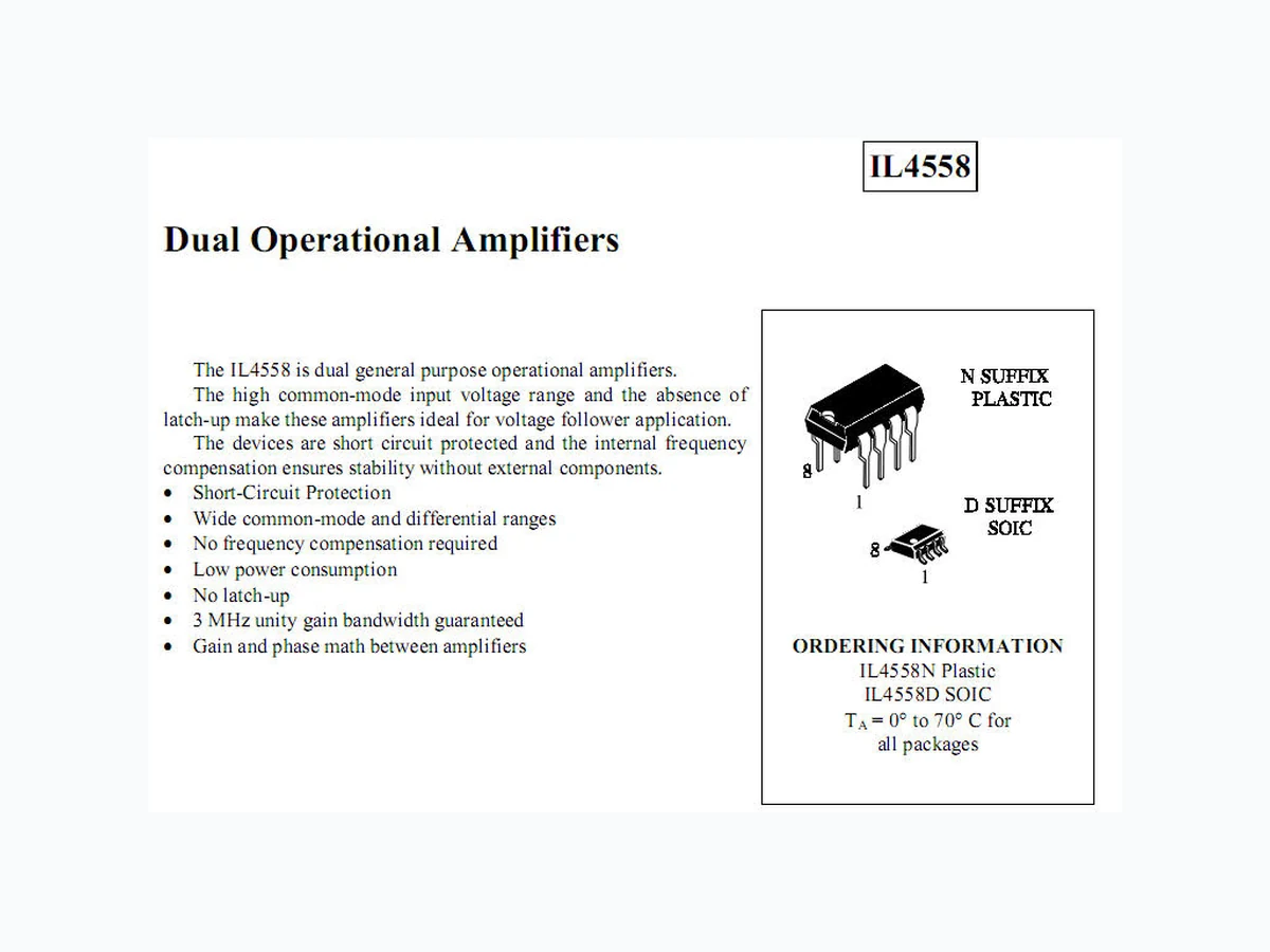
Y sTEK 1.4558 Dual Operational Amplifiers The IL4558 is dual general purpose operational amplifiers. NN SUFFIX The high common-mode input voltage range and the absence of PLASTIC latch-up make these amplifiers ideal for voltage follower application. The devices are short circuit protected and the internal frequency compensation ensures stability without external components. a . rec Cosay Protection ; 1 D SUFFIX © Wide common-mode and differential ranges rece © No frequency compensation required 2G © Low power consumption 1 ¢ No latch-up e 3 MHz unity gain bandwidth guaranteed ¢ Gain and phase math between amplifiers ORDERING INFORMATION IL4558N Plastic IL4558D SOIC Ta= 0° to 70° C for all packages PIN ASSIGNMENT Alle sf ve a q2 70B a3 6B via 5} BY LOGIC DIAGRAM , =i i2 Inverting Input A Noninverting Input At —3 1 Output A _ . 5 7 Noninverting Input B Output B 1 - 6 Tnverting Input B Pin 4 = Supply Voltage V_ Pin 8 = Supply Voltage V- ee
MAXIMUM RATINGS® [_symbot [Parameter | Value nit] Storage Temperature Range -55 to +125 * Maximum Ratings are those values beyond which damage to the device may occur. Functional operation should be restricted to the Recommended Operating Conditions. RECOMMENDED OPERATING CONDITIONS [somber [Parmeter «in Mas | Ua] This device contains protection circuitry to guard against damage due to high static voltages or electric fields. However, precautions must be taken to avoid applications of any voltage higher than maximum rated voltages to this high-impedance circuit. For proper operation, Vj and Vout should be constrained to the range GNDS(Vjy or Vour)$ Vee. Unused inputs must always be tied to an appropriate logic voltage level (e.g., either GND or Ve). Unused outputs must be left open. a
ELECTRICAL CHARACTERISTICS(1,= 0 to +70°C, V'= +15 V, V'=-15 V) Symbol Test Conditions Unit [atin [typ [Max | | Vio | mpurofier Voltage | Rsstoxo | | 8.0 | mv | | to | ipurofsercunenst | STS 200 | tw | impurBiasCument | STS S00 [| m | | Av | Large-Signal VolugeGain [R.22KQ,ve=zlov [| 9 [ [| viv | Vou | Output Voltage Swing [xewxe [ze { | | v | | ww [pees ee oe A Fe Range eee fee TTT Ratio fees fee Ratio [rr [SupplyCunent TCS 8 [oma | [sr [SiewRae —[Ri=2KQ TS] STC | | Pe | PowerConsumprion [== | || 0 | mw | Pe freer ite [TL | f=30 Hz -30 KHz [Tews [SouneCument | 20 TT | [tex [SinkCunent TE C™C~—C—~sC TEs TYPICAL PERFORMANCE CURVES Vops* Ri = vay 5 "(=e LOOM. 11m g » va Hees Co
3 Bes od ae |
ze a | . ied a | ; of ZC A E > | | g (ZL g 7 LAT TM TTT ; | 1 pb 8 om xe itt mM ie oo Lid J » PREQUENCY f (Hz) LOAD RESISTANCE R, (kQ) Vuief Vom > Vee: Ver a
a ee <J a Nl h ts pes rt Sted ee ae Ze mime ~~. Ss g LL SP RRAN ey A go ROAKARAASA Ss | | J KN NIA a ™ Seni ee o>RRAAAASAAN
5 LU eee : Cl SSSR KINI
EEE EH ait TTT tt PEAY S33 1 3 n El i mw tk 6 a x 12 4 (s FRQUENCY f (Hz) SUPPLY VOLTAGE V*, V"(#V) Vopge f 1-T, Pmt et TTT TTT
7 COCO
f "yuu E PTT TTT tty tt tt iN e LOCOCO a Eee ; »COLCPCCEeeceeerr} n m ik im wk ™ an 4 D mn © FRQUENCY f (Hz) AMBIENT TEMPERATURE T, (°C) Schematic Diagram (Each Amplifier) vte 7 Vv, - q ; - wt I. -_ Output Ue 2 | | rl y--__iT a