
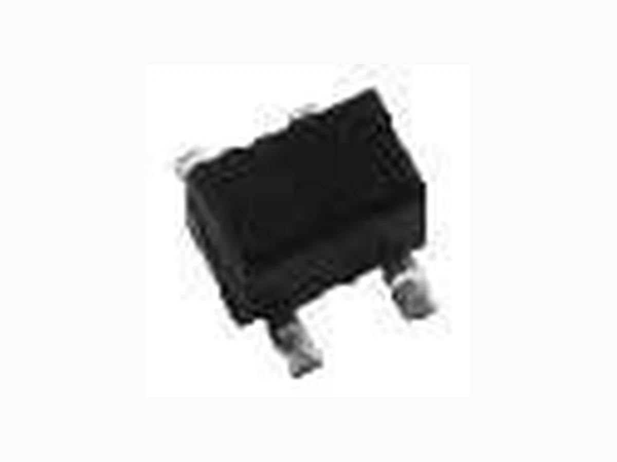
hw109a ETC
Document overview
- Manufacturer or author: Provided By www.digicamel.com(FREE DATASHEET DOWNLOAD SITE)
- PDF pages: 2
Technical content
- Absolute Maximum Ratings
- Electrical Characteristics(Ta=25˚C)
- Dimensional Drawing (mm)
- Classification of Output Hall Voltage (VH ) Input Voltage(V) Input Current(mA) Note : When ordering, specify 3-rank or wider range(e·g·,BCD).
- Input Current Derating Curve
- Input Voltage Derating Curve N ote : For constant-voltage drive, stay w ithin this input voltage derating curve envelope. N ote : R in of H all elem ent decreases rapidly as am bient tem perature increases. Ensure com pliance w ith input current derating curve envelope, throughout the operating tem perature range. 0–60 –40 –20 0 20 40 60 80 100 120 Input Resistance R in : 250 to 450 2.0 1.0 0–60 –40 –20 0 20 40 60 80 100 120 HW-109A
- H igh-sensitivity InSb H all elem ent.
- SM T package w ith sensing area leaned 45˚.
- Shipped in packet-tape reel (5000pcs per reel). Item Symbol Topr. Tstg. Ic Const. Current Drive Limit –40 to +125 –40 to +110 Unit mA Pinning ConditionsVH [ mV ]Rank B=50mT, Vc=IV Constant Voltage Drive Max. Input Current Operating Temp. Range Storage Temp. Range Dielectric Strength Output Hall Voltage Input Resistance Output Resistance Offset Voltage Temp. Coefficient of VH Temp. Coefficient of Rin Item 100V D.C Const. Voltage Drive B=50mT, Vc=IV B=0mT, Ic=0.1mA B=0mT, Ic=0.1mA B=0mT, Vc=IV B=50mT, Ic=5mA B=0mT, Ic=0.1mA Conditions 1.0 122 250 250 Min. M mV mV %/˚C %/˚C Unit –1.8 –1.8 Typ. 450 320 450 Max. 1(±) 3 (±)Input 4(±)2 (±)Output A 122 to 150 B 144 to 174 C 168 to 204 D 196 to 236 F 266 to 320 E 228 to 274 Input Resistance R in : 250 to 450 0.35±0.2 0.1 0 to 0.1 0.851.76 N 1.45±0.1 2.7±0.2 2.1±0.1 1.30.4 0.3 1.35±0.10.65 0.7 3 2 VH R in R out Vos VH R in Symbol Notes : 1. VH = VHM – Vos (VHM:meter indication) 2. VH = X X 100 3. Rin = X X 100R in (T1) (T3 – T2) VH (T3) – VH (T2) (T3 – T2) R in (T3) – Rin (T2) VH (T1) T1 = 20˚C, T2 = 0˚C, T3 = 40˚C Ambient Temperature.(˚C) Ambient Temperature.(˚C) Note : It is requested to read and accept "IMPORTANT NOTICE". Please be aw are that AKE products are not intended for use in life support equipm ent, devices, or system s. U se of AKE products in such applications requires the advance w ritten approval of the appropriate AKE officer. C ertain applications using sem iconductor devices m ay involve potential risks of personal injury, property dam age, or loss of life. In order to m inim ize these risks, adequate design and operating safeguards should be provided by the custom er to m inim ize inherent or procedural hazards. Inclusion of AKE products in such applications is understood to be fully at the risk of the custom er using AKE devices or system s.
- Characteristic Curves –50 0 50 100 150 2000 1750 1500 1250 1000 750 500 250 Ic Vin –50 0 50 100 150 Ic Vin 600.0 500.0 400.0 300.0 200.0 100.0 0.0 0 10 20 30 40 50 Ic Vin 1200 1000 800 600 400 200 5 10 15 20 Ic Vin 5 10 15 20 Ic Vin a c f i 2000 1800 1600 1400 1200 1000 800 600 400 200 -50 0 50 100 150 VH -B VH -Vc, VH -IcVH -T VOS -Vc, VOS -IcVOS -T *Magnetic Flux Density 1(mT)=10(G) R in-T Ambient Temperature(˚C) Magnetic Flux Density B (mT) Ambient Temperature(˚C) Ambient Temperature(˚C) Output Voltage:VH (mV )Offset Voltage:Vos(mV ) Ic (mA) Input Current Vc (V) Input Voltage Ic (mA) Input Current Vc (V) Input Voltage Ic:(mA) Vc:(V) Ic:(mA) Vc:(V) Ic const Vc const Ic = 5 (mA) Vc = 1 (V) Ta = 25 (˚C) Ic const Vc const B = 50 (mT) Ta = 25 (˚C) Ic const Vc const B = 0 (mT) Ta = 25 (˚C) Ic const Vc const Ic = 5 (mA) Vc = 1 (V) B = 0 (mT) Ic const Vc const Output Voltage:VH (mV )Output Voltage:VH (mV )Offset Voltage:Vos(mV ) Ic = 5 (mA) Vc = 1 (V) B = 50 (mT) HW-109A Input Resistance:Rin( ) In This Example : Rin=350( ), Vos=4.7(mV), Vc=1(V)