
HVLED001.fm
Document overview
- Manufacturer or author: STMICROELECTRONICS
- PDF pages: 27
Technical content
Datasheet sections
- 1 Block diagram
- 2 Typical application - HP F flyback
- 3 Pin settings
- 4 Electrical data
- 4.1 Absolute maximum ratings
- 4.2 Thermal data
- 5 Electrical characteristics
- 6 Typical electrical characteristi cs
- 7 Application information
- 7.1 Operating modes
- 7.1.1 Start-up mode
- 7.1.2 Active mode
- 7.1.3 Stop mode
- 7.1.4 Low consumption mode
- 7.1.5 Soft-start
- 7.2 Control loop
- 7.2.1 Current sense input
- 7.2.2 Feedback input
- 7.2.3 Zero current detection
- 7.2.4 Primary side regulation feature
- 7.2.5 Burst-mode operation
- 7.3 Gate driver
- 7.4 IC supply management
- 7.4.1 VCC supply management
- 7.4.2 High voltage start-up
- 7.5 Autorestart timer (ART)
Features
Quasi-resonant (QR) topology Primary side regulation of output voltage Direct optocoupler connection for current loop regulation with feedback disconnection detection and disable 800 V high voltage start-up High power factor and low THD in universal range High efficiency and output stability in wide voltage and current range Low start-up and quiescent current Programmable minimum off time Integrated input voltage detection for high power factor capability and protection triggering Latch free device guarantee by smart autoreload timer (ART) 0 - 10 and PWM dimming compatible Remote control pin
Applications
Single stage LED drivers with high power factor up to 75 W Two stages LED drivers up to 150 W
Description
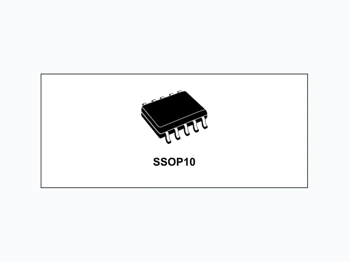
The HVLED001 is an enhanced peak current mode controller capable of controlling mainly high power factor (HPF) flyback or buck-boost topologies in LED drivers having an output power up to 150 W. Some other topologies, like buck, boost and SEPIC can also be implemented. ST’s innovative high voltage technology allows direct connection of the HVLED001 to the input voltage in order to both start up the device and monitor the input voltage without the need for external components. Advanced features are embedded to control either the output voltage or output current precisely and reliably using a reduced number of components, mainly passive. Startup and light- load conditions are managed by dedicated operating schemes to improve the quality of output variable regulation in the final application. Abnormal conditions such as open circuit, output short-circuit, input overvoltage/undervoltage, and circuit failures such as open loop and overcurrent of the main switch are effectively controlled. A smart auto-recover timer (ART) function is built in to guarantee automatic application recovery, without loss of reliability. SSOP10 Table 1. Device summary
Obsolete Product(s) - Obsolete Product(s)
1 Block diagram
Figure 1. Block diagram
2 Typical application - HPF flyback
Figure 2. Typical application
3 Pin settings
Figure 3. Pin connection Table 2. Pin description High voltage start-up and input voltage detection. CC pin and GND pin during the start-up and low consumption. blanking time is obtained leaving the pin unconnected. and / or to the compensation network related to the output voltage primary side regulation loop. An upper threshold VOFP detects a failure of the optocoupler. The burst-mode and disable conditions are also related to the voltage applied to this pin. CTRL 5 This pin is used to disable the IC and generate the soft-start ramp. External active circuitry can be used to turn off the application. side regulation and the input voltage for brownout detection. generate the triggering signal when not externally available (e.g.: start-up). Input to the current sense comparator for the power regulation. saturation) and, on this occurrence, activates the second level overcurrent protection procedure.
The output stage is able to drive the power MOSFET's and IGBT's gate. driving or signal processing. mounted as close as possible to the device) are connected between this pin and GND. Internal clamp structure prevents accidental low energy spikes damaging the device. Table 2. Pin description (continued)
4 Electrical data
4.1 Absolute maximum ratings
4.2 Thermal data
Table 3. Absolute maximum ratings Table 4. Thermal data
5 Electrical characteristics
Tj = Ta = 25 °C production tested, VCC = 15 V, unless otherwise specified. Table 5. Electrical characteristics
Table 5. Electrical characteristics (continued)
- Operating conditions not associat ed with specific production test.
- Parameters in tracking group 1.
- Parameters not tested in production.
- Parameters in tracking group 2.
- kp parameter includes the overall tolerances of the multiplier block defined as per note 8.
- Parameters in tracking group 3.
- VHVSU,pk indicates the maximum value of VHVSU.
- TBLANK = MAX {koff • (VTOFF,fix - VTOFF)}.
- Parameters in tracking group 4.
6 Typical electrical characteristics
Figure 4. Graph 1: VCC current consumption
7 Application information
7.1 Operating modes
constant current applications (LED drivers). Application schematics of the two main topologies are reported in Figure 5 and Figure 6. Figure 5. High power factor flyback - constant output current
Figure 6. High power factor flyback – primary side regulated constant output voltage
7.1.1 Start-up mode
During this state the CTLR pin is internally pulled to ground.
Figure 7. Initial start-up phase
7.1.2 Active mode
parameter in the closed loop (peak current control method). VCC,su threshold. The HVSU is inactive during the active mode.
7.1.3 Stop mode
consumption is not minimized and the soft-start procedure is not enabled.
7.1.4 Low consumption mode
disabling condition is removed. unit (HVSU) delivering Icharge to the output capacitor. must be decoupled using a 1N4148 diode.
7.1.5 Soft-start
a capacitor placed between the CTRL pin and GND defines the soft-start time. and analog disable (AN_DIS) are ignored.
7.2 Control loop
resonant valley following the primary side demagnetization input. A detail of the block involved into this scheme is shown in Figure 8. Figure 8. Control loop blocks
7.2.1 Current sense input
The peak of the primary current is read across a shunt resistor placed between the MOSFET's source and compared with a threshold equal to: Equation 1 Where the term VHVSU,pk is the maximum value of the HVSU voltage within around 20 ms and is used to compensate the dependency on the input voltage of the open loop gain transfer function. The gain k p collects all the proportional terms between the HVSU voltage and CS threshold. A leading edge blanking time (LEB) is applied after MOSFET's turn on. The Vcs signal is upper limited to a value that depends on the CTRL voltage and is lower limited to a level defined as: Equation 2 V CS,min = VHVSU • 0.15 A second level OCP threshold is present to temporarily stop the switching activity in case of inductor saturation.
7.2.2 Feedback input
The FB pin is intended to be connected directly to the collector of the optocoupler that provides the galvanic insulation to the control loop as well as to act as compensation output for the primary side control (PSR) loop of the output voltage (see Section 7.2.4). A suitable RC network can be placed between FB and ground to compensate the control loop. In case of constant output voltage applications, the PSR loop can be used to regulate the output voltage saving the secondary side error amplifier. The FB voltage is also used as an input parameter for the burst-mode operation described in Section 7.2.5. The pin embeds protection to prevent from the operation with the failed optocoupler and can be pulled to ground to interrupt the switching activity (stop mode).
7.2.3 Zero current detection
The zero level detection is performed by a trigger logic that, once armed by a rising voltage, is sensitive to falling edges. The advanced ZCD logic is able to discriminate between the normal operation, output short-circuit or start-up condition. An internal blanking time prevents any triggering signal to activate the MOSFET's at the very beginning of the off time, where spurious resonances could be present. As a result, the first falling edge occurring after the blanking time turns on the MOSFET. To ensure a proper operation, the transformer has to be designed to guarantee that the inductor's demagnetization time is longer than TBLANK (at VTOFF > VTOFF,fix) when the V CS value (Equation 1: ) is higher than 0.3 V (typ.). VCS kp VHVSU VHVSU pk Obsolete Product(s) - Obsolete Product(s)
a fixed blanking time is provided. The TBLANK value depends on Toff voltage (Figure 9). Figure 9. TBLANK voltage vs Tblank time (typical) The ZCD pin embeds a negative clamp to limit the negative-going current.
7.2.4 Primary side regulation feature
of this loop is internally fixed to VREF,PSR and applied to the non-inverting input of the E/A. compensation network has to be connected.
Figure 10. PSR E/A small signal model
7.2.5 Burst-mode operation
used or by the internal error amplifier if the PSR operation is on.
7.3 Gate driver
power can be greater than 150 W.
7.4 IC supply management
different operating conditions.
7.4.1 VCC supply management
VCC voltage above the technological constraints. order to meet energy saving regulation. necessary to properly sustain the Vcc voltage during all operating phases.
7.4.2 High voltage start-up
the VCC pin and maintain the IC responsive during low consumption modes. a burst on the stage's input. it sources a minimum current (Icharge,su) to charge the VCC pin up to Vcc,su threshold. threshold. At this occurrence the active mode is invoked and the HVSU is turned off. During other active mode's phases and the stop mode the HVSU is off. If the low consumption mode is entered, the HVSU unit is turned on. Table 6 summarizes the HVSU behavior in all IC conditions. Table 6. HVSU operating modes
7.5 Autorestart timer (ART)
The autorestart timer unit is responsible for the generation of the protection's intervals and of the restart times after the low consumption mode. A summary of all possible combination of times is described in each protection paragraph.
7.6 Protections
A comprehensive set of protections is embedded to ensure a high level of reliability of the final application using a limited number of components.
7.6.1 Overcurrent protection (OCP)
To prevent any damage to active components in case of inductor's saturation the MOSFET is immediately turned off by the fast OCP protection. At this occurrence the IC temporarily enters the stop state for a time equal to TOCP.
7.6.2 Input overvoltage protection (I-OVP)
Disturbances of the input voltage like surges or bursts may increase the voltage applied to the transformer primary side. Worst, an excessive input voltage could be applied to the application. These occurrences may result into MOSFET damage during the off-state when the drain voltage rises to Vin plus reflected voltage, eventually above the maximum absolute rating of the MOSFET itself. An input voltage higher than VSurge, measured by HVSU structure, immediately stops the IC. If the extra voltage diminishes before Tsurge the device restarts immediately without activating the start-up procedure, otherwise the low consumption mode is entered until the input voltage returns below the safety threshold. An internal hysteresis improves the noise rejection of this feature. In the latter case the ART activates the start-up procedure.
7.6.3 Brownout protection (BO)
The current sourced by the ZCD pin's negative clamp during on time is compared to a minimum value to determine whether the input voltage is lower than the input range specification (brownout protection). If a value lower than IBO for a time longer than TBO, managed by the ART, is detected, the IC is stopped for Trec and then restarted. When the protection is triggered, the ART performs the autorelaoding procedure after Trec. The brownout protection is active during the active mode, but blanked during the soft-start.
7.6.4 Optocoupler failu re protection (OFP)
This protection detects either the absence of the optocoupler control (no pull-down) or the overload condition for more than a time equal to TOFP and switches off the application putting the device in the low consumption mode. This prevents the output power from rising above excessive values due to the loss of control. The ART manages the TOFP interval and performs the auto-reloading procedure after Trec. The OFP is active during the active mode, but blanked during the soft-start. Obsolete Product(s) - Obsolete Product(s)
7.7 Disable and monitor feature
Several disabling means are available to externally disable the IC: 1. Driving FB pin low (FB_DIS): this occurrence immediately stops the switching activity until the FB voltage returns above the threshold. 2. Driving CTRL pin low (CTRL_DIS): this occurrence immediately puts the device in the low consumption mode; when the CTLR pin is left free, the internal biasing mean pulls-up the voltage above the threshold entering the soft-start procedure. 3. Driving CTRL pin high (AN_DIS): a CTRL voltage higher than the threshold for a time longer than Tdis causes the device to enter the low consumption mode. The ART timer performs an auto-recover procedure after Trec. Anytime the HVLED001 device enters low consumption, an internal pull-down discharges the soft-start capacitor and resets the soft-start time. Obsolete Product(s) - Obsolete Product(s)
8 Package information
specifications, grade definitions and product status are available at: www.st.com. Figure 11. SSOP10 package outline
Table 7. SSOP10 package mechanical data
9 Revision history
Table 8. Document revision history 13-Jan-2015 1 Initial release.