
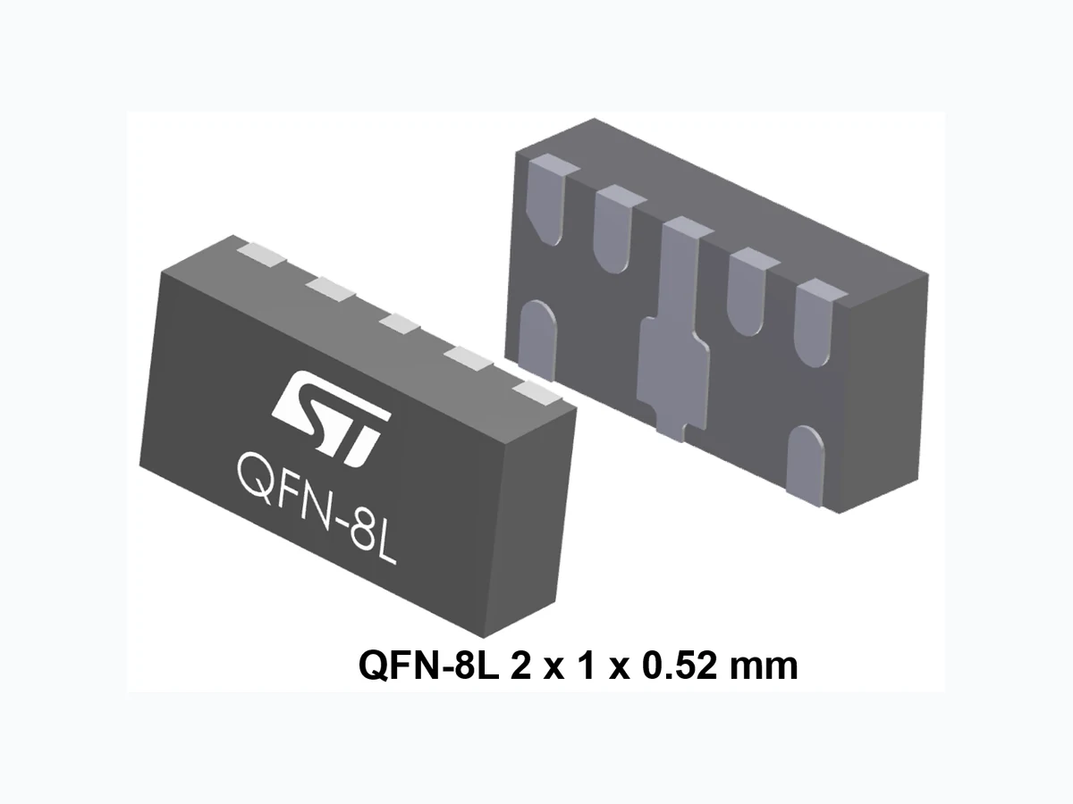
Datasheet - HSP061-4NY8 - 3 V 4-line high speed port protection in QFN-8L
Document overview
- Manufacturer or author: STMICROELECTRONICS
- PDF pages: 12
Technical content
Features
- Large bandwidth: 6 GHz
- Low capacitance: 0.5 pF
- Operating junction temperature range: -40 °C to 150 °C
- RoHS compliant and halogen free
- Complies with IEC 61000-4-2, exceeds level 4 : – ±8 kV (contact discharge) – ±20 kV (air discharge)
Applications
- USB 5Gbps
- USB 10Gbps
- HDMI 2.1
- FPD-Link III
- GMSL
- 1000BASE-T1
- APIX3
Description
The HSP061-4NY8 is a 4-line low capacitance TVS designed to protect high-speed interfaces with differential lines in industrial and consumer applications. Electro-static discharge (ESD) capability is compliant with system level ESD standard IEC 61000-4-2, and then with the low energy ESD component level standards such as human body model (HBM), and charge device model (CDM). The large bandwidth is compatible with USB 5Gbps, USB 10Gbps, HDMI 2.1 - 12Gbps, FPD-Link III 4 - 16Gbps, GMSL 3 - 12Gbps, 1000BASE-T1, APIX3 6Gbps. The device is packaged in a 8-pin QFN of 2 mm x 1.0 mm with a nominal height of 0.52 mm. Product status link HSP061-4NY8
3 V 4-line high speed port protection in QFN-8L
DS6809 - Rev 6 - February 2024 For further information contact your local STMicroelectronics sales office.
1 Characteristics
Table 1. Absolute maximum ratings (Tamb = 25 °C) Table 2. Electrical characteristics (Tamb = 25 °C)
1.1 Characteristics (curves)
Figure 1. Leakage current versus junction temperature Figure 2. ESD response to IEC 61000-4-2 Figure 3. ESD response to IEC 61000-4-2 Figure 4. S21 attenuation Figure 5. HDMI2.1 - 12 Gbps per channel without device Figure 6. HDMI2.1 - 12 Gbps per channel with device (with
2 Package information
In order to meet environmental requirements, ST offers these devices in different grades of ECOPACK packages, depending on their level of environmental compliance. ECOPACK specifications, grade definitions and product status are available at: www.st.com. ECOPACK is an ST trademark.
2.1 QFN-8L package information
Figure 10. QFN-8L package outline
- Values in inches are converted from mm.
Package information
2.2 Packing and marking information
Figure 11. Marking layout Figure 12. Package orientation in reel Figure 13. Tape leader and trailer dimensions Figure 14. Tape and reel orientation Figure 15. Reel dimensions (mm) Figure 16. Inner box dimensions (mm)
Figure 17. Tape outline Table 4. Tape and reel mechanical data
3 Recommendation on PCB assembly
3.1 Recommended footprint and stencil opening
Figure 18. Recommended footprint and stencil opening (µm)
3.2 PCB design
- To control the solder paste amount, closed vias are recommended instead of open vias.
- A symmetrical layout is recommended.
Figure 19. Recommended printed circuit board layout
3.3 Solder paste
- Halide-free flux qualification ROL0 according to ANSI/J-STD-004.
- “No clean” solder paste is recommended.
- Offers a high tack force to resist component movement during high speed.
- Solder paste with fine particles: powder particle size is 20-38 μm.
3.4 Placement
- Manual positioning is not recommended.
- It is recommended to use the lead recognition capabilities of the placement system, not the outline centering
- Standard tolerance of ±0.05 mm is recommended.
- 1.0 N placement force is recommended. Too much placement force can lead to squeezed out solder paste
and solder paste that could cause open solder joints or badly centered packages.
- To improve the package placement accuracy, a bottom side optical control should be performed with a high
- For assembly, a perfect supporting of the PCB (all the more on flexible PCB) is recommended during solder
paste printing, pick and place and reflow soldering by using optimized tools.
3.5 Reflow profile
Figure 20. ST ECOPACK® recommended soldering reflow profile for PCB mounting Note: Minimize air convection currents in the reflow oven to avoid component movement. Note: Maximum soldering profile corresponds to the latest IPC/JEDEC J-STD-020.
4 Ordering information
Table 5. Ordering information
- The marking can be rotated by multiples of 90° to differentiate assembly location.
Ordering information
Revision history
Table 6. Document revision history 20-Apr-2010 1 Initial release. Updated values for ∆CI/O - GND in Table 2. Updated Figure 13. 29-Mar-2012 3 Updated Table 2. Updated weight value in Table 4. 27-Mar-2013 5 Added notes on marking rotation. Document reworked to improve readability. Updated USB and HDMI eyes diagrams.
IMPORTANT NOTICE – READ CAREFULLY STMicroelectronics NV and its subsidiaries (“ST”) reserve the right to make changes, corrections, enhancements, modifications, and improvements to ST products and/or to this document at any time without notice. Purchasers should obtain the latest relevant information on ST products before placing orders. ST products are sold pursuant to ST’s terms and conditions of sale in place at the time of order acknowledgment. Purchasers are solely responsible for the choice, selection, and use of ST products and ST assumes no liability for application assistance or the design of purchasers’ products. No license, express or implied, to any intellectual property right is granted by ST herein. Resale of ST products with provisions different from the information set forth herein shall void any warranty granted by ST for such product. ST and the ST logo are trademarks of ST. For additional information about ST trademarks, refer to www.st.com/trademarks. All other product or service names are the property of their respective owners. Information in this document supersedes and replaces information previously supplied in any prior versions of this document. © 2024 STMicroelectronics – All rights reserved HSP061-4NY8 DS6809 - Rev 6 page 12/12