

 Download PDF
HS7541A SIPEX
Document overview
- PDF pages: 7
Technical content
Page 1
12–Bit CMOS Multiplying DAC
I ±0.5 LSB DNL and INL I High Stability, Segmented Architecture (3 MSB’s) I Proprietary, Low TCR Thin–Film Resistor Technology I Low Sensitivity to Output Amplifier Offset I 2KV ESD Protection on All Digital Inputs I Operates With +5V to +15V Power Supplies I AD7541/7541A Replacement I Low Cost
DESCRIPTION…
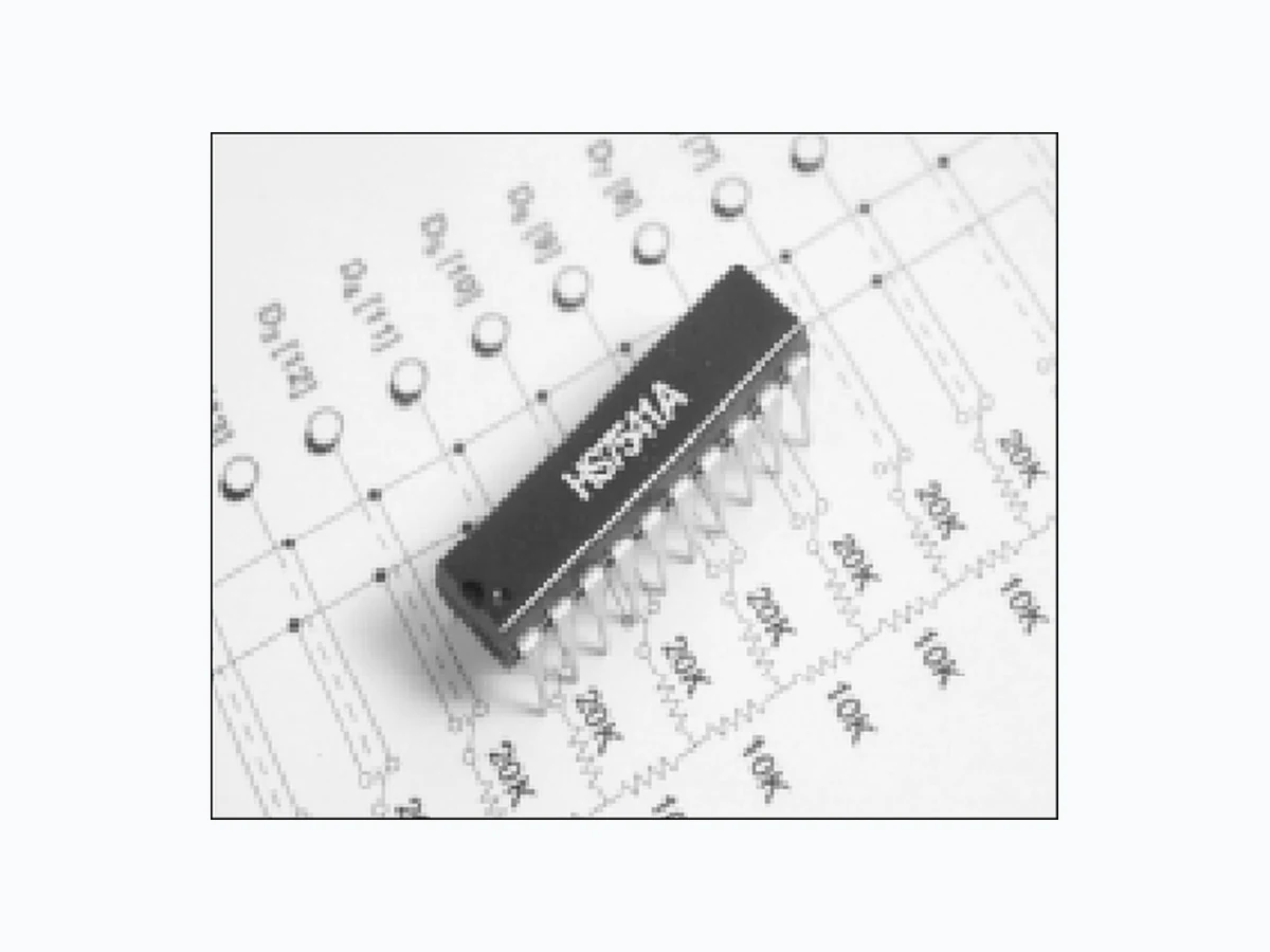
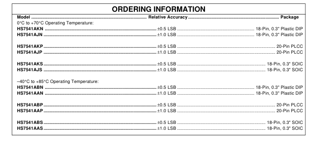
The HS7541A is a low–cost, high stability monolithic 12–bit CMOS 4–quadrant multiplying DAC. It is constructed using a proprietary low–TCR thin–film process that requires no laser–trimming to achieve 12–bit performance. The HS7541A is a superior pin–compatible replacement for the industry standard 7541 and AD7541A. It is available in both commercial and industrial temperature ranges. It operates with +5V to +15V power supply voltages. It is available in 18– pin plastic DIP and SOIC, and 20–pin PLCC packages.
Page 2
ABSOLUTE MAXIMUM RATINGS
(TA = 25°C unless otherwise noted.) These are stress ratings only and functional operation of the device at these or any other above those indicated in the operation
sections of the specifications below is not implied. Exposure to absolute maximum rating conditions for extended periods of time may affect reliability.
VDD to GND .................................................................. –0.3V, +17V Digital Input Voltage to GND ................................. –0.3V, VDD+0.3V VREF or VRFB to GND ................................................................ ±25V Output Voltage (Pin 1, Pin 2) ................................ –0.3V, VDD+0.3V Power Dissipation (Any Package to +75°C) ........................ 450mW Derates above 75°C by ...................................................... 6mW/°C Dice Junction Temperature ................................................. +150°C Storage Temperature ............................................ –65°C to +150°C Lead Temperature (Soldering, 60 seconds) ........................ +300°C
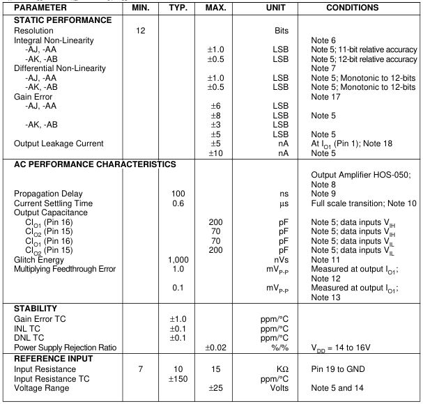
SPECIFICATIONS
(TA=25°C; VDD =+15V, VREF = +10V; IO1 = IO2 = GND = 0V; unipolar unless otherwise noted.)
ESD (ElectroStatic Discharge) sensitive device. Permanent damage may occur on unconnected devices subject to high energy electrostatic fields. Unused devices must be stored in conductive foam or shunts. Personnel should be properly grounded prior to handling this device. The protective foam should be discharged to the destination socket before devices are removed.
Page 3
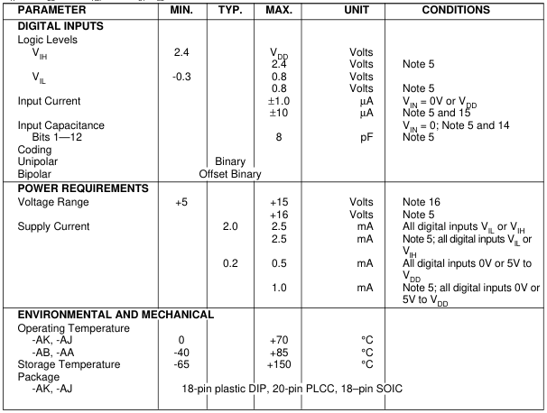
SPECIFICATIONS (continued)
(TA=25°C; VDD =+15V, VREF = +10V; IO1 = IO2 = GND = 0V; unipolar unless otherwise noted.)
Notes and Cautions: Do not apply voltages higher than VDD or less than GND potential on any terminal other than VREF or VRFB. 1. The digital inputs are diode-clamp protected against ESD damage. However, permanent damage may occur 2. on unprotected units from high-energy electrostatic fields. Keep units in conductive foam at all times until ready to use. 3. Use proper anti-static handling procedures. Stresses above those listed under “Absolute Maximum Ratings” may cause permanent damage to the 4. device. This is a stress rating only and functional operation at or above these specifications is not implied. Exposure to the above maximum rated conditions for extended periods may affect device reliability.
- From TMIN to TMAX. Integral Non-linearity is measured as the arithmetic mean value of the magnitudes of the greatest positive 6. deviation and the greatest negative deviation from the theoretical value of any given input combination. Differential Non-linearity is the deviation of an output step from the theoretical value of 1 LSB for any two 7. adjacent digital input codes. AC performance characteristics are included for design guidance only and are subject to sample testing only. 8. RL = 100Ω, CEXT = 13pF; all data inputs 0V to VDD or VDD to 0V; from 50% digital input change to 90% of final 9. analog output. Settling to ±0.01% FSR (strobed); all data inputs 0V to VDD or VDD to 0V.
- VREF = 0V, DAC register alternatively loaded with all 0’s and all 1’s. 11. 12. VREF = 20VP-P; F = 10kHz sinewave. 13. VREF = 20VP-P; F = 1kHz sinewave. 14. Guaranteed by design, but not production tested. Logic inputs are MOS gates. IIN typically is less than 1nA @ 25°C. 15. 16. Accuracy is guaranteed at VDD = +15V only. Measured using internal feedback resistor with DAC loaded with all 1’s. 17. 18. All digital inputs = 0V.
Page 4
PIN ASSIGNMENTS
18–Pin Plastic DIP and SOIC Pin 1 — IO1 — Inverted Current Output. Pin 2 — IO2 — Current Output. Pin 3 — GND — Analog Ground. Pin 4 — D11 (MSB) — Data Bit 11 (Most Significant Bit). Pin 5 — D10 — Data Bit 10. Pin 6 — D9 — Data Bit 9. Pin 7 — D8 — Data Bit 8. Pin 8 — D7 — Data Bit 7. Pin 9 — D6 — Data Bit 6. Pin 10 — D5— Data Bit 5. Pin 11 — D4— Data Bit 4. Pin 12 — D3— Data Bit 3. Pin 13 — D2— Data Bit 2. Pin 14 — D1— Data Bit 1. Pin 15 — D0 (LSB) — Data Bit 0 (Least Significant Bit). Pin 16 — VDD— +5V to +15V Power Supply. Pin 17 — VREF— Voltage Reference Input. Pin 18 — RFB— Feedback Resistor.
20–Pin Plastic LCC Pin 1 — IO1 — Inverted Current Output. Pin 2 — IO2 — Current Output. Pin 3 — GND — Analog Ground. Pin 4 — N.C. — No Connection. Pin 5 — D11 (MSB) — Data Bit 11 (Most Significant Bit). Pin 6 — D10 — Data Bit 10. Pin 7 — D9 — Data Bit 9. Pin 8 — D8 — Data Bit 8. Pin 9 — D7 — Data Bit 7. Pin 10 — D6 — Data Bit 6. Pin 11 — D5— Data Bit 5. Pin 12 — D4— Data Bit 4. Pin 13 — D3— Data Bit 3. Pin 14 — D2— Data Bit 2. Pin 15 — D1— Data Bit 1.
Pin 16 — D0 (LSB) — Data Bit 0 (Least Significant Bit). Pin 17 — N.C. — No Connection. Pin 18 — VDD— +5V to +15V Power Supply. Pin 19 — VREF— Voltage Reference Input. Pin 20 — RFB— Feedback Resistor.
FEATURES…
The HS7541A is a low–cost, high stability monolithic 12–bit CMOS 4–quadrant multiplying DAC. It is constructed using a proprietary low– TCR thin–film process that requires no laser– trimming to achieve 12–bit performance. With its inherent high stability and a segmented (de- coded) DAC architecture, the HS7541A retains its performance over time and temperature. To further improve reliability, all digital inputs are protected against 2KV ESD. Each DAC is fully characterized by all–codes testing to eliminate any hidden errors.
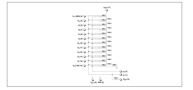
The HS7541A consists of a highly stable thin– film R–2R ladder network and twelve NMOS current switches (please refer to the Block Diagram on the first page of this data sheet). The switches are temperature compensated, and their “on” resistances are binarily scaled so that the voltage drop across each switch is identical, which contributes to the stability of the DAC. The internal feedback resistor used in the output current–to–voltage conversion by an external op amp is matched to the R–2R ladder.
CIRCUIT DESCRIPTION
General The HS7541A is a 12-bit multiplying D/A converter consisting of a highly stable, SiChrome thin-film R-2R resistor ladder network, and twelve pairs of NMOS current-steering switches on a monolithic chip.
A simplified circuit of the HS7541A is shown in Figure 1. The R-2R inverted ladder binarily divides the input currents that are switched between the IOUT1 and IOUT2 bus lines. This switching allows a constant current to be maintained in each ladder leg independent of the input code.
Page 5
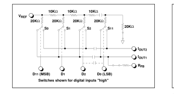
Figure 1. Simplified DAC Circuit
The twelve output current-steering switches are in series with the R-2R ladder, and therefore, can introduce bit errors. It is essential then, that the switch “on” resistance be binarily scaled so that the voltage drop across each switch remains constant. If, for example, switch S0 of Figure 1 was designed with an “on” resistance of 10 ohms, switch S1 for 20 ohms, etc., then with a 10V reference input, the current through S0 is 0.5mA, S1 is 0.25mA, etc.; a constant 5mV drop will then be maintained across each switch.
To further insure accuracy across the full temperature range, permanently “on” MOS switches are included in series with the feedback resistor and the R-2R ladder’s terminating resistor. These series switches are equivalently scaled to two times switch S11 (MSB) and to switch S0 (LSB) respectively to maintain constant relative voltage drops with varying temperature. During any testing of the resistor ladder or RFB (such as incoming inspection), VDD must be present to turn “on” these series switches.
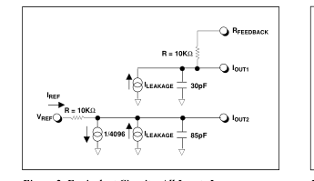
Figure 2. Equivalent Circuit – All Inputs Low
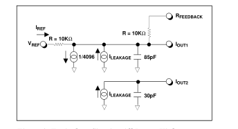
Figure 3. Equivalent Circuit – All Inputs High
2001V ESD Protection In the design of the HS7541A’s data inputs, 2001V ESD resistance has been incorporated through careful layout and the inclusion of input protection circuitry.
Equivalent Circuit Analysis Figures 2 and 3 show the equivalent circuits for all digital inputs LOW and HIGH respectively. The reference current is switched to IOUT2 when all inputs are LOW, and to IOUT1 when all inputs are HIGH. The ILEAKAGE current source is the combination of surface and junction leakages to the substrate; the 1/4096 current source represents the constant 1-bit current drain through the ladder terminating resistor. The output capacitance is dependent upon the digital input code, and therefore varies between the low and high values.
Output Impedance The output resistance, as in the case of the output capacitance, varies with the digital input code. The resistance, looking back into the IOUT1 ter-
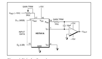
Figure 4. Unipolar Operation
Page 6
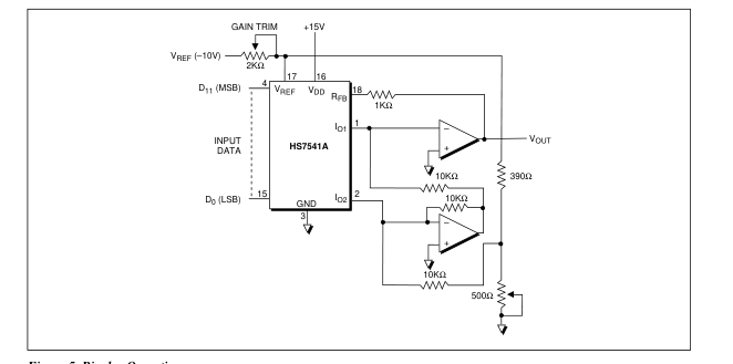
Figure 5. Bipolar Operation
minal, may be anywhere between 10kΩ (the feedback resistor alone when all digital inputs are LOW) and 7.5kΩ (the feedback resistor in parallel with approximately 30kΩ of the R-2R ladder network resistance when any single bit is HIGH). Static accuracy and dynamic performance will be affected by these variations.
UNIPOLAR OPERATION
Figure 4 shows the connections to implement digital unipolar operation of the HS7541A. The reference voltage applied to VREF (pin17) may be positive or negative. The 2KΩ potentiometer tied to VREF, and the 1KΩ resistor in the feedback loop are both optional; they are needed only when gain error must be trimmed to less than 0.3% FSR. They should track each other to better than 0.1%. It is not necessary that they track the resistors internal to the HS7541A.
| DIGITAL INPUT | I 0UT |
| 1111 1111 1111 | -0.99975 x V REF |
| 1000 0000 0000 | -0.50000 x V REF |
| 0111 1111 1111 | -0.49975 x V REF |
| 0000 0000 0000 | 0V |
Table 1. Unipolar Input Coding
As shown in the figure, the output current of the HS7541A is typically connected to an external op amp, with its non-inverting input tied to ground. The amplifier should be selected for low input bias current and low drift over temperature. To maintain the specified linearity, the amplifier’s input offset voltage should be mulled to less than ±200µV (0.1 LSB).
BIPOLAR OPERATION
Figure 5 shows the connections for bipolar operation of the HS7541A. The digital input coding is offset binary as shown in Table 2. As is the case for unipolar operation, the gain trim resistors can be omitted if minimum gain error is not required. The op amp selection criteria and offset nulling are the same as for unipolar operation.
| DIGITAL INPUT | I 0UT |
| 1111 1111 1111 | -0.99951 x V REF |
| 1000 0000 0001 | -0.00049 x V REF |
| 1000 0000 0000 | 0V |
| 0100 0000 0000 | +0.50000 x V REF |
| 0000 0000 0000 | +1.00000 x V REF |
Table 2. Bipolar Input Coding
Page 7
SIGNAL PROCESSING EXCELLENCE
Sipex Corporation
Headquarters and Sales Office 22 Linnell Circle Billerica, MA 01821 TEL: (978) 667-8700 FAX: (978) 670-9001 e-mail: sales@sipex.com
Sales Office 233 South Hillview Drive Milpitas, CA 95035 TEL: (408) 934-7500 FAX: (408) 935-7600
Sipex Corporation reserves the right to make changes to any products described herein. Sipex does not assume any liability arising out of the application or use of any product or circuit described hereing; neither does it convey any license under its patent rights nor the rights of others.