
 Download PDF
HS7512 SIPEX
Document overview
- PDF pages: 6
Technical content
Page 1
SP7512 and HS3120
Corporation
Double–Buffered 12-Bit Multiplying DAC
I Monolithic Construction I 12–Bit Resolution I 0.01% Non-Linearity I Four–Quadrant Multiplication I Latch-up Protected I Low Power – 30mW I Single +15V Power Supply
DESCRIPTION…
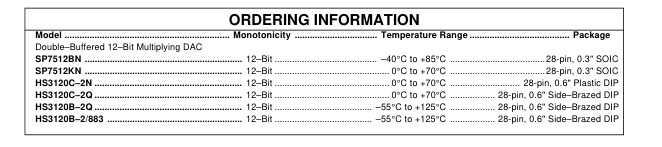
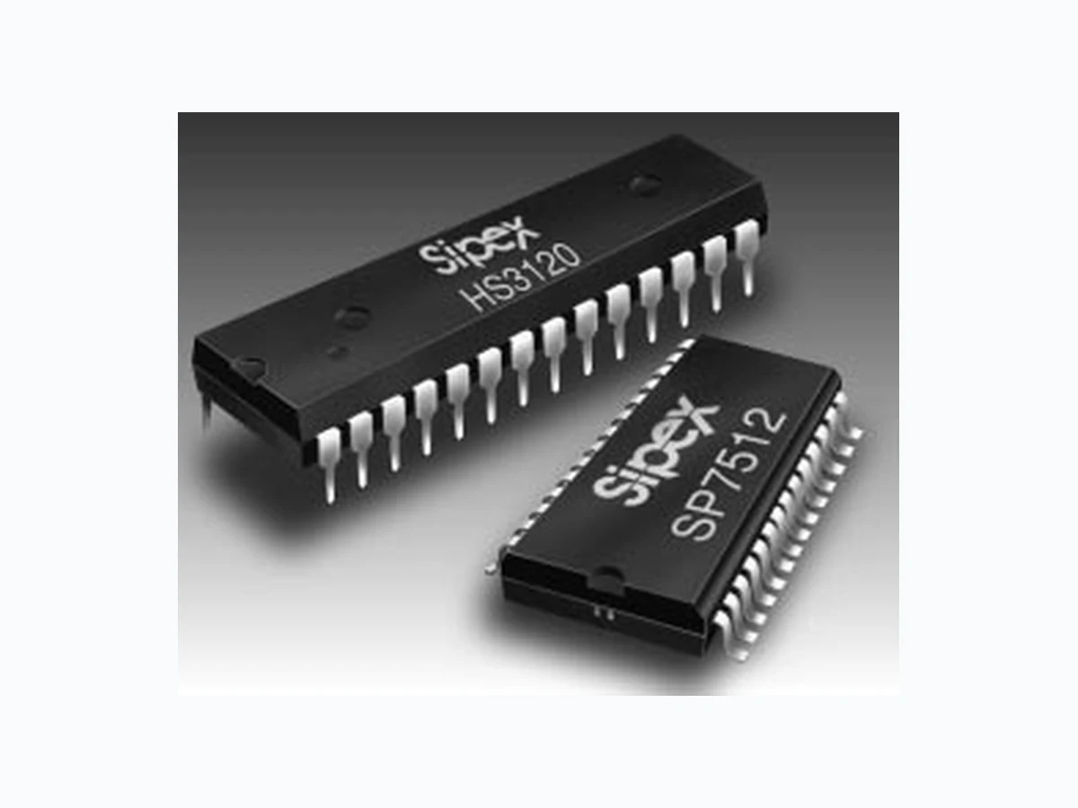
The SP7512 and HS3120 are precision 12-bit multiplying DACs, double–buffered for easy interfacing with microprocessor busses. Both unipolar and bipolar operation can be accommodated with a minimum of external components. The SP7512 is available for use in commercial and industrial temperature ranges, packaged in a 28-pin SOIC. The HS3120 is available in commercial and military temperature ranges, packaged in a 28–pin side–brazed DIP.
Page 2
SPECIFICATIONS
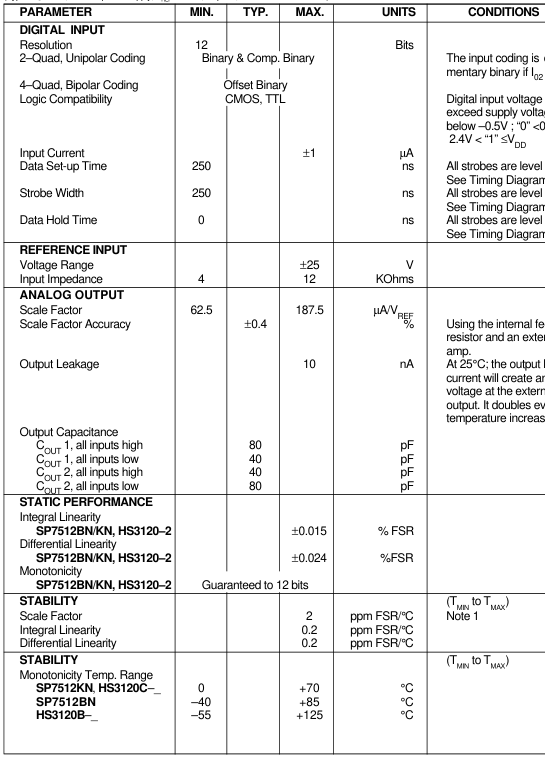
(Typical @ 25°C, nominal power supply, VREF = +10V, unipolar, unless otherwise noted)
voltage at the external op amps
Page 3
SPECIFICATIONS (continued)
(Typical @ 25°C, nominal power supply, VREF = +10V, unipolar unless otherwise noted)
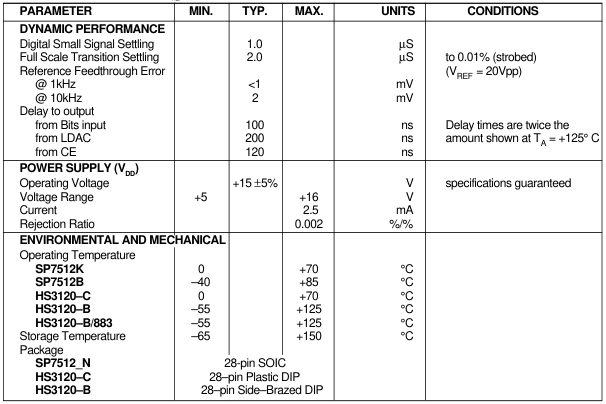
Notes: Using the internal feedback resistor, output leakage current creates an offset, which doubles every 1. 10°C rise in temperature.
Page 4
PIN ASSIGNMENTS
Pin 1 – FB4 – Feedback Bipolar Operation Pin 2 – LDTR – Ladder Termination Pin 3 – FB3 – Feedback Bipolar Operation Pin 4 – VREF – Reference Voltage Input Pin 5 – FB1 – Feedback, Unipolar/Bipolar Pin 6 – IO1 – Current out into virtual ground Pin 7 – IO2 – Current out-complement of I01 Pin 8 – VSS – Ground, Analog and DAC Register Pin 9 – DB11 – MSB, Data Bit 1 Pin 10 – DB10 – Data Bit 2 Pin 11 – DB9 – Data Bit 3 Pin 12 – DB8 – Data Bit 4 Pin 13 – DB7 – Data Bit 5 Pin 14 – DB6 – Data Bit 6 Pin 15 – DB5 – Data Bit 7 Pin 16 – DB4 – Data Bit 8 Pin 17 – DB3 – Data Bit 9 Pin 18 – DB2 – Data Bit 10 Pin 19 – DB1 – Data Bit 11 Pin 20 – DB0 – LSB, Data Bit 12 Pin 21 – LDAC – Transfers data from input to
DAC register; a logic “0” latches data into registers; a logic “1” allows data to change (transfer to) register. Pin 22 – CE – Chip Enable, active low Pin 23 – LBE – Bit 12 to Bit 9 Enable Pin 24 – MBE – Bit 8 to Bit 5 Enable Pin 25 – HBE – Bit 4 to Bit 1 Enable Pin 26 – VDD2 – Supply Analog and DAC Register Pin 27 – VSS1 – Ground input latches Pin 28 – VDD1 – Supply input latches NOTE: Pins 8 and 27, and pins 26 and 28 must be connected externally.
FEATURES…
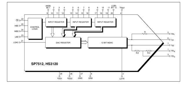
The SP7512 and HS3120 are precision 12-bit multiplying DACs with internal two-stage input storage registers for easy interfacing with mi- croprocessor busses. The DACs are implemented as a one-chip CMOS circuit with a resistor ladder network designed for 0.01% linearity without laser trimming.
The input registers are sectioned into 3 segments of 4 bits each, all individually addressable. The DAC-register, following the input registers, is a parallel 12-bit register for holding the DAC data while the input registers are up- dated. Only the data held in the DAC register determines the analog output value of the converter.
The SP7512 and HS3120 have been designed for great flexibility in connecting to bus-oriented systems. The 12 data inputs are organized into 3 independent addressable 4-bit input registers such that the DACs can be connected to either a 4, 8 or 16-bit data bus. The control logic of the DACs includes chip enable and latch enable inputs for flexible memory mapping. All controls are level-triggered to allow static or dynamic operation.
A total of 5 output lines are provided on the DACs to allow unipolar and bipolar output connection with a minimum of external components. The feedback resistor is internal. The resistor ladder network termination is externally available, thus eliminating an external resistor for the 1 LSB offset in bipolar mode.
The SP7512 is available for use in commercial and industrial temperature ranges, packaged in
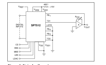
Figure 1. Unipolar Operation
Page 5
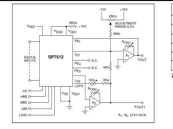
Figure 2. Bipolar Operation
a 28–pin SOIC. The HS3120 is available in commercial and military temperature ranges, packaged in a 28–pin side–brazed DIP. For product processed and screened to the requirements of MIL–M–38510 and MIL–STD–883C, please consult the factory (HS3120B only).
APPLICATIONS INFORMATION
Unipolar Operation Figure 1 shows the interconnections for unipolar operation. Connect IO1 and FB1 as shown in diagram. Tie IO2 (Pin 7), FB3 (Pin 3), and FB4 (Pin 1) to Ground (Pin 8). To maintain specified linearity, external amplifiers must be zeroed. This is best done with VREF set to zero and, with the DAC register loaded with all bits at zero, adjust ROS for VOUT = 0V
| TRANSFER FUNCTION (N=12) | ||
| BINARY INPUT | UNIPOLAR OUTPUT | BIPOLAR OUTPUT |
| 111...111 | –V (1 – 2–N) REF | –V (1 – 2 –(N – 1)) REF |
| 100...001 | –V (1/2 + 2–N) REF | –V (2 –(N – 1)) REF |
| 100...000 | –V /2 REF | 0 |
| 011...111 | –V (1/2 – 2–N) REF | V (2 –(N – 1)) REF |
| 000...000 | 0 | V REF |
Table 1. Transfer Function
Bipolar Operation Figure 2 shows the interconnections for bipolar operation. Connect IO1, IO2, FB1, FB3, FB4 as shown in diagram. Tie LDTR to IO2. To maintain specified linearity, external amplifiers must be zeroed. This is best done with VREF set to zero and, the DAC register loaded with 10...0 (MSB = 1), set ROS2 for VOUT1 = 0V. Then set ROS1 for VOUT = 0V.
Grounding Connect all GND pins to system analog ground and tie this to digital ground. All unused input pins must be grounded.
Page 6
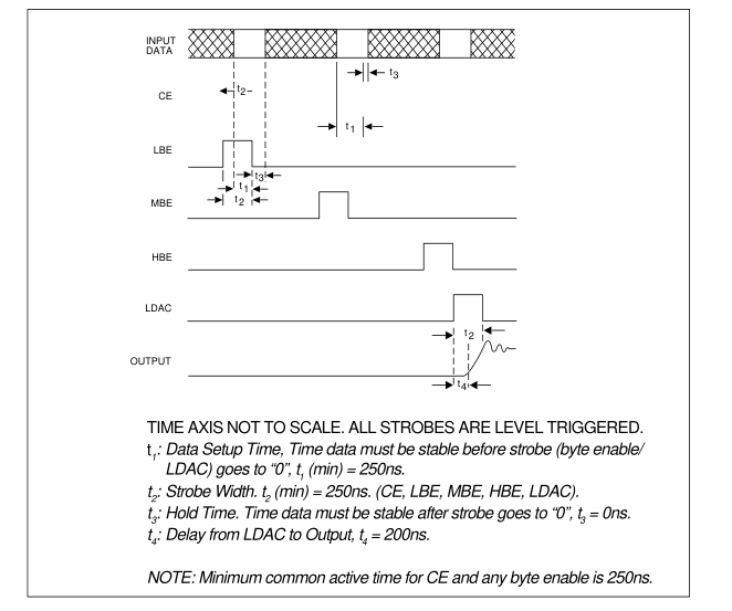
TIMING