


 Download PDF
HGT1S20N36G3VL FAIRCHILD
Document overview
- PDF pages: 7
Technical content
Page 1
HGTP20N36G3VL,HGT1S20N36G3VLS,
March 2004
Features
- Logic Level Gate Drive
- Internal Voltage Clamp
- ESD Gate Protection
- TJ = 175oC
- Ignition Energy Capable
Description
This N-Channel IGBT is a MOS gated, logic level device which is intended to be used as an ignition coil driver in automotive ignition circuits. Unique features include an active voltage clamp between the collector and the gate which provides Self Clamped Inductive Switching (SCIS) capability in ignition circuits. Internal diodes provide ESD protection for the logic level gate. Both a series resistor and a shunt resistor are provided in the gate circuit.
PACKAGING
| PART NUMBER | PACKAGE | BRAND |
|---|---|---|
| HGTP20N36G3VL | TO-220AB | 20N36GVL |
| HGT1S20N36G3VL | TO-262AA | 20N36GVL |
| HGT1S20N36G3VLS | TO-263AB | 20N36GVL |
The development type number for this device is TA49296.
Absolute Maximum Ratings TC = +25oC, Unless Otherwise Specified
HGT1S20N36G3VL
20A, 360V N-Channel,
Logic Level, Voltage Clamping IGBTs
Packages
JEDEC TO-220AB
E CG
COLLECTOR
(FLANGE)
JEDEC TO-263AB
COLLECTOR
(FLANGE)
G
E
JEDEC TO-262AA
ECG
COLLECTOR
(FLANGE)
Symbol
COLLECTOR
R1
GATE
R2
EMITTER
HGTP20N36G3VL
HGT1S20N36G3VL
HGT1S20N36G3VLS
UNITS
Collector-Emitter Bkdn Voltage At 10mA, RGE = 1kΩ. . . . . . . . . . . . . . . . . . . . . . . BVCER
395
V
Emitter-Collector Bkdn Voltage At 10mA . . . . . . . . . . . . . . . . . . . . . . . . . . . . . . . . BVECS
28
V
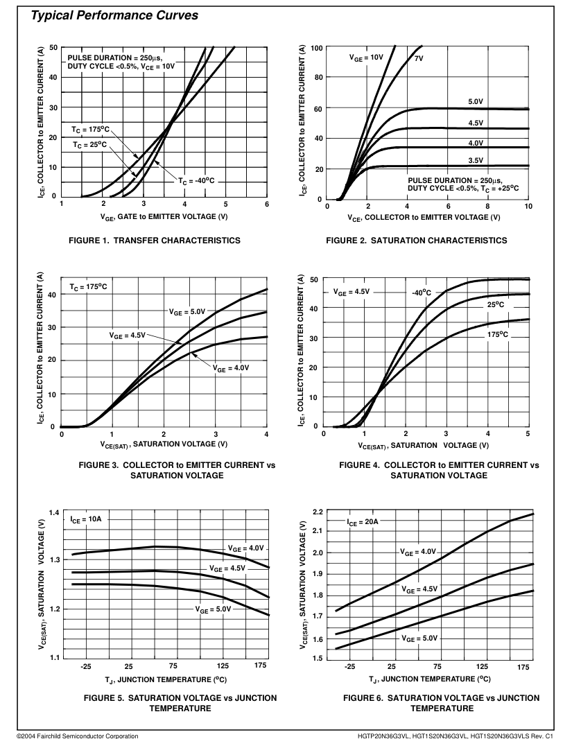
Collector Current Continuous At VGE = 5.0V, TC = +25oC, Figure 7 . . . . . . . . . . . . . IC25
37.7
A
At VGE = 5.0V, TC = +100oC . . . . . . . . . . . . . . . . . . . .IC100
26
A
Gate-Emitter-Voltage (Note) . . . . . . . . . . . . . . . . . . . . . . . . . . . . . . . . . . . . . . . . . . . VGES
±10
V
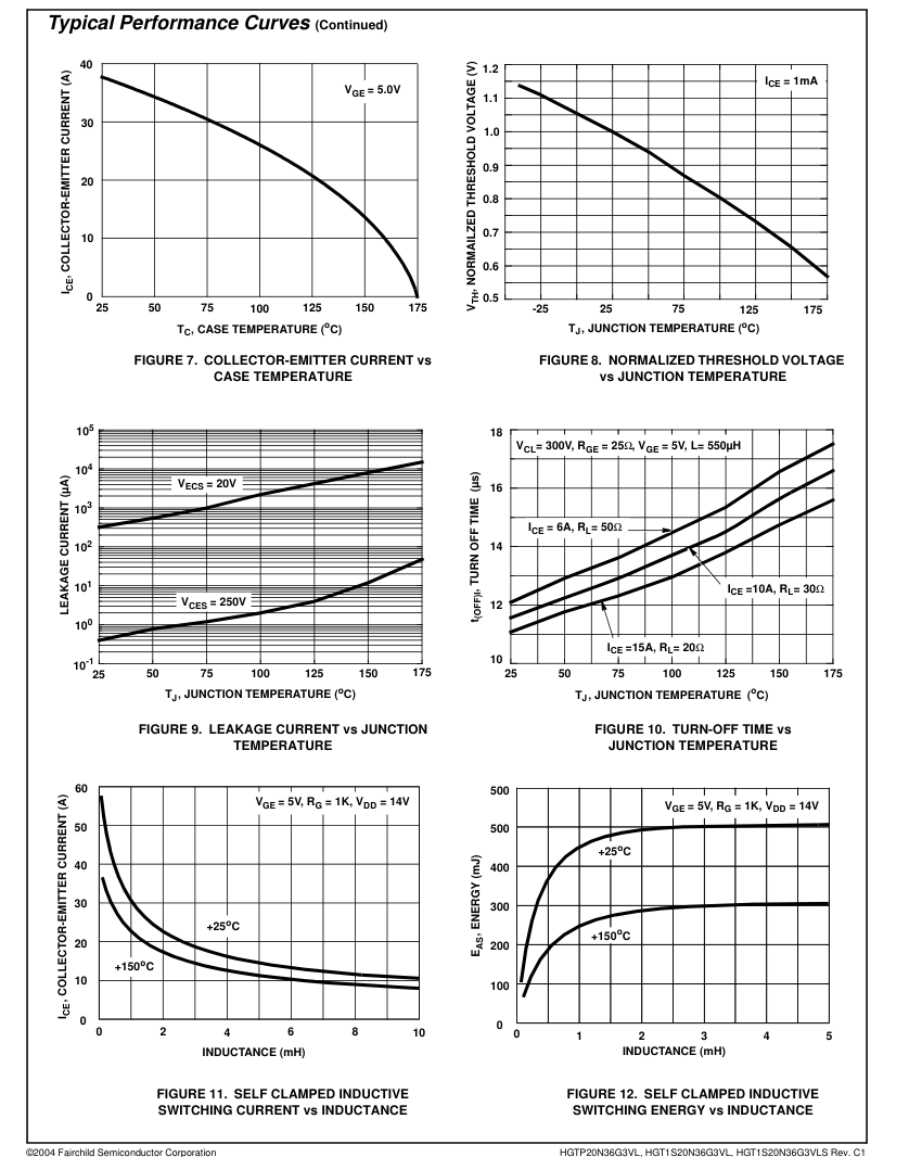
Inductive Switching Current At L = 2.3mH, TC = +25o C . . . . . . . . . . . . . . . . . . . . . .ISCIS
21
A
At L = 2.3mH, TC = +150oC . . . . . . . . . . . . . . . . . . . . . .ISCIS
16
A
Collector to Emitter Avalanche Energy At L = 2.3mH, TC = +25oC . . . . . . . . . . . . . . EAS
500
mJ
Power Dissipation Total At TC = +25oC . . . . . . . . . . . . . . . . . . . . . . . . . . . . . . . . . . . . PD
150
W
Power Dissipation Derating TC > +25oC. . . . . . . . . . . . . . . . . . . . . . . . . . . . . . . . . . . . . . .
W/oC
1.0
Operating and Storage Junction Temperature Range . . . . . . . . . . . . . . . . . . . . .TJ, TSTG
oC
-40 to +175
Maximum Lead Temperature for Soldering . . . . . . . . . . . . . . . . . . . . . . . . . . . . . . . . . .TL
oC
Electrostatic Voltage at 100pF, 1500Ω. . . . . . . . . . . . . . . . . . . . . . . . . . . . . . . . . . . . ESD
KV
NOTE: May be exceeded if IGEM is limited to 10mA.
Page 2
Electrical Specifications TC = +25oC, Unless Otherwise Specified
| PARAMETERS | SYMBOL | TEST CONDITIONS | LIMITS | UNITS | |||
|---|---|---|---|---|---|---|---|
| MIN | TYP | MAX | |||||
| Collector-Emitter Breakdown Voltage | BV CES | I = 10mA, C V = 0V GE | T = +175oC C | 345 | 380 | 415 | V |
| T = +25oC C | 355 | 385 | 415 | V | |||
| T = -40oC C | 355 | 390 | 425 | V | |||
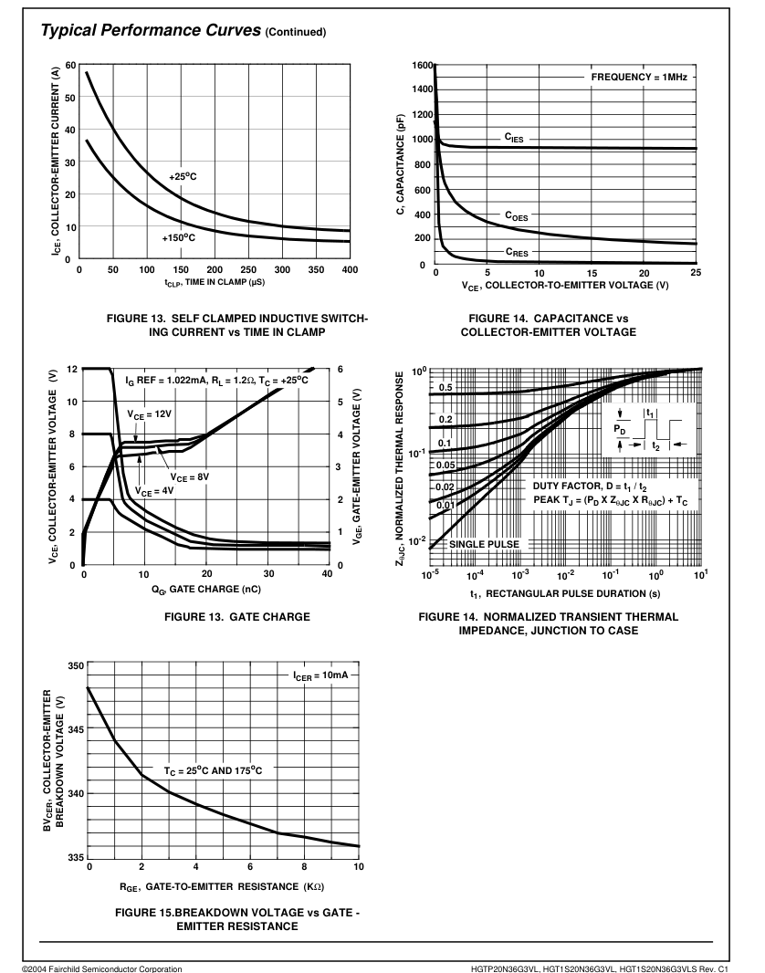
| Collector-Emitter Breakdown Voltage | BV CER | I = 10mA C V = 0V GE R = 1kΩ GE | T = +175oC C | 320 | 360 | 395 | V |
| T = +25oC C | 335 | 365 | 395 | V | |||
| T = -40oC C | 335 | 370 | 410 | V | |||
| Gate-Emitter Plateau Voltage | V GEP | I = 10A C V = 12V CE | T = +25oC C | - | 3.7 | - | V |
| Gate Charge | Q G(ON) | I = 10A C V = 5V GE V = 12V CE | T = +25oC C | - | 28.7 | - | nC |
| Collector-Emitter Clamp Breakdown Voltage | BV CE(CL) | I = 10A C R = 1KΩ G | T = +175oC C | 330 | 360 | 415 | V |
| Emitter-Collector Breakdown Voltage | BV ECS | I = 10mA C | T = +25oC C | 28 | 36 | - | V |
| Collector-Emitter Leakage Current | I CES | V = 250V CE | T = +25oC C | - | - | 5 | µA |
| V = 250V CE | T = +175oC C | - | - | 250 | µA | ||
| Emitter-Collector Leakage Current | I ECS | V = 24V EC | T = +25oC C | - | - | 1.0 | mA |
| Collector-Emitter Saturation Voltage | V CE(SAT) | I = 10A C V = 4.5V GE | T = +25oC C | - | 1.3 | 1.6 | V |
| T = +175oC C | - | 1.25 | 1.5 | V | |||
| I = 20A C V = 5.0V GE | T = +25oC C | - | 1.6 | 1.9 | V | ||
| T = +175oC C | - | 1.9 | 2.4 | V | |||
| Gate-Emitter Threshold Voltage | V GE(TH) | I = 1mA C V = V CE GE | T = +25oC C | 1.1 | 1.6 | 2.3 | V |
| Gate Series Resistance | R 1 | T = +25oC C | - | 75 | - | Ω | |
| Gate-Emitter Resistance | R 2 | T = +25oC C | 10 | 20 | 30 | kΩ | |
| Gate-Emitter Leakage Current | I GES | V = ±10V GE | ±330 | ±500 | ±1000 | µA | |
| Gate-Emitter Breakdown Voltage | BV GES | I = ±2mA GES | ±12 | ±14 | - | V | |
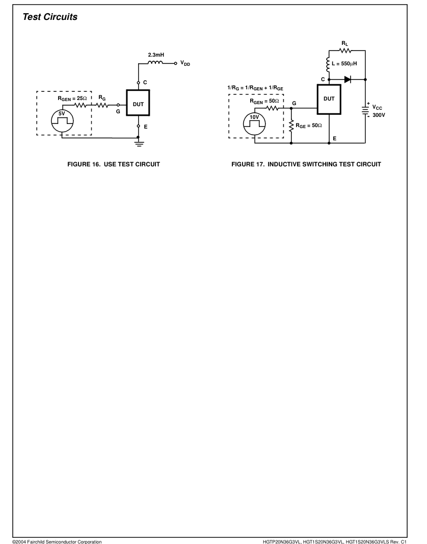
| Current Turn-Off Time-Inductive Load | t + D(OFF)I t F(OFF)I | I = 10A, R = 25Ω, C G L = 550µH, R = 26.4Ω, V = 5V, L GE V = 300V, T = +175oC CL C | - | 15 | 30 | µs | |
| Inductive Use Test | I SCIS | L = 2.3mH, V = 5V, G R = 1KΩ G | T = +150oC C | 16 | - | - | A |
| T = +25oC C | 21 | - | - | A | |||
| Thermal Resistance | R θJC | - | - | 1.0 | oC/W | ||
Page 3
Page 4
Page 5
Page 6
Page 7
TRADEMARKS
The following are registered and unregistered trademarks Fairchild Semiconductor owns or is authorized to use and is not intended to be an exhaustive list of all such trademarks.
ISOPLANAR™
Stealth™
ACEx™
POP™
FACT Quiet Series™
SuperFET™
ActiveArray™
Power247™
LittleFET™
FAST
MICROCOUPLER™
PowerSaver™ SuperSOT™-3
Bottomless™
FASTr™
PowerTrench
SuperSOT™-6
CoolFET™
MicroFET™
FPS™
QFET
SuperSOT™-8
CROSSVOLT™
MicroPak™
FRFET™
MICROWIRE™
DOME™
GlobalOptoisolator™
EcoSPARK™
MSX™
GTO™
E2CMOS™
MSXPro™
HiSeC™
EnSigna™
OCX™
I2C™
FACT™
OCXPro™
ImpliedDisconnect™
OPTOLOGIC
Across the board. Around the world.™
SyncFET™
QS™
QT Optoelectronics™ TinyLogic
TINYOPTO™
Quiet Series™
TruTranslation™
RapidConfigure™
UHC™
RapidConnect™
SILENT SWITCHER UltraFET
OPTOPLANAR™
VCX™
SMART START™
The Power Franchise
SPM™
PACMAN™
Programmable Active Droop™
DISCLAIMER
FAIRCHILD SEMICONDUCTOR RESERVES THE RIGHT TO MAKE CHANGES WITHOUT FURTHER NOTICE TO ANY PRODUCTS HEREIN TO IMPROVE RELIABILITY, FUNCTION OR DESIGN. FAIRCHILD DOES NOT ASSUME ANY LIABILITY ARISING OUT OF THE APPLICATION OR USE OF ANY PRODUCT OR CIRCUIT DESCRIBED HEREIN; NEITHER DOES IT CONVEY ANY LICENSE UNDER ITS PATENT RIGHTS, NOR THE RIGHTS OF OTHERS.
LIFE SUPPORT POLICY
FAIRCHILD’S PRODUCTS ARE NOT AUTHORIZED FOR USE AS CRITICAL COMPONENTS IN LIFE SUPPORT DEVICES OR SYSTEMS WITHOUT THE EXPRESS WRITTEN APPROVAL OF FAIRCHILD SEMICONDUCTOR CORPORATION. As used herein: 1. Life support devices or systems are devices or systems which, (a) are intended for surgical implant into the body, or (b) support or sustain life, or (c) whose failure to perform when properly used in accordance with instructions for use provided in the labeling, can be reasonably expected to result in significant injury to the user.
PRODUCT STATUS DEFINITIONS
Definition of Terms
- A critical component is any component of a life support device or system whose failure to perform can be reasonably expected to cause the failure of the life support device or system, or to affect its safety or effectiveness.
| Datasheet Identification | Product Status | Definition |
| Advance Information | Formative or In Design | This datasheet contains the design specifications for product development. Specifications may change in any manner without notice. |
| Preliminary | First Production | This datasheet contains preliminary data, and supplementary data will be published at a later date. Fairchild Semiconductor reserves the right to make changes at any time without notice in order to improve design. |
| No Identification Needed | Full Production | This datasheet contains final specifications. Fairchild Semiconductor reserves the right to make changes at any time without notice in order to improve design. |
| Obsolete | Not In Production | This datasheet contains specifications on a product that has been discontinued by Fairchild semiconductor. The datasheet is printed for reference information only. |
Rev. I9