


 Download PDF
HGTP20N35G3VL INTERSIL
Document overview
- PDF pages: 6
Technical content
Page 1
April 1995
Features
- Logic Level Gate Drive
- Internal Voltage Clamp
- ESD Gate Protection
- TJ = 175oC
- Ignition Energy Capable
Description
This N-Channel IGBT is a MOS gated, logic level device which is intended to be used as an ignition coil driver in automotive ignition circuits. Unique features include an active voltage clamp between the collector and the gate which provides Self Clamped Inductive Switching (SCIS) capability in ignition circuits. Internal diodes provide ESD protection for the logic level gate. Both a series resistor and a shunt resistor are provided in the gate circuit.
PACKAGING AVAILABILITY
| PART NUMBER | PACKAGE | BRAND |
|---|---|---|
| HGTP20N35G3VL | T0-220AB | 20N35GVL |
| HGT1S20N35G3VL | T0-262AA | 20N35GVL |
| HGT1S20N35G3VLS | T0-263AB | 20N35GVL |
NOTE: When ordering, use the entire part number. Add the suffix 9A to obtain the TO-263AB variant in the tape and reel, i.e., HGT1S20N35G3VLS9A. The development type number for this device is TA49076.
Absolute Maximum Ratings TC = +25oC, Unless Otherwise Specified
HGTP20N35G3VL,
HGT1S20N35G3VL,
HGT1S20N35G3VLS
20A, 350V N-Channel,
Logic Level, Voltage Clamping IGBTs
Packages
JEDEC TO-220AB
COLLECTOR
EMITTER
GATE
COLLECTOR
(FLANGE)
JEDEC TO-262AA
EMITTER
COLLECTOR
GATE
COLLECTOR
(FLANGE)
JEDEC TO-263AB
COLLECTOR
(FLANGE)
GATE EMITTER
Terminal Diagram
N-CHANNEL ENHANCEMENT MODE
COLLECTOR
R1
GATE
R2
EMITTER
HGTP20N35G3VL
HGT1S20N35G3VL
HGT1S20N35G3VLS
UNITS
Collector-Emitter Bkdn Voltage At 10mA, RGE = 1kΩ. . . . . . . . . . . . . . . . . . . . . . . BVCER
375
V
Emitter-Collector Bkdn Voltage At 10mA . . . . . . . . . . . . . . . . . . . . . . . . . . . . . . . . BVECS
24
V
Collector Current Continuous At VGE = 5.0V, TC = +25oC, Figure 7 . . . . . . . . . . . . . IC25
20
A
At VGE = 5.0V, TC = +100oC . . . . . . . . . . . . . . . . . . . .IC100
20
A
Gate-Emitter-Voltage (Note). . . . . . . . . . . . . . . . . . . . . . . . . . . . . . . . . . . . . . . . . . . VGES
±10
V
Inductive Switching Current At L = 2.3mH, TC = +25o C . . . . . . . . . . . . . . . . . . . . . ISCIS
26
A
At L = 2.3mH, TC = +175oC . . . . . . . . . . . . . . . . . . . . . ISCIS
18
A
Collector to Emitter Avalanche Energy At L = 2.3mH, TC = +25oC . . . . . . . . . . . . . . EAS
775
mJ
Power Dissipation Total At TC = +25oC . . . . . . . . . . . . . . . . . . . . . . . . . . . . . . . . . . . . PD
150
W
Power Dissipation Derating TC > +25oC. . . . . . . . . . . . . . . . . . . . . . . . . . . . . . . . . . . . . .
W/oC
1.0
Operating and Storage Junction Temperature Range . . . . . . . . . . . . . . . . . . . . .TJ, TSTG
oC
-40 to +175
Maximum Lead Temperature for Soldering . . . . . . . . . . . . . . . . . . . . . . . . . . . . . . . . . .TL
oC
Electrostatic Voltage at 100pF, 1500Ω. . . . . . . . . . . . . . . . . . . . . . . . . . . . . . . . . . . . ESD
KV
NOTE: May be exceeded if IGEM is limited to 10mA.
CAUTION: These devices are sensitive to electrostatic discharge; follow proper IC Handling Procedures.
File Number 4006
1-888-INTERSIL or 321-724-7143 | Copyright © Intersil Corporation 1999
3-66
Page 2
Specifications HGTP20N35G3VL, HGT1S20N35G3VL, HGT1S20N35G3VLS
Electrical Specifications TC = +25oC, Unless Otherwise Specified
| PARAMETERS | SYMBOL | TEST CONDITIONS | LIMITS | UNITS | |||
|---|---|---|---|---|---|---|---|
| MIN | TYP | MAX | |||||
| Collector-Emitter Breakdown Voltage | BV CES | I = 10mA, C V = 0V GE | T = +175oC C | 310 | 345 | 380 | V |
| T = +25oC C | 320 | 350 | 380 | V | |||
| T = -40oC C | 320 | 355 | 390 | V | |||
| Collector-Emitter Breakdown Voltage | BV CER | I = 10mA C V = 0V GE R = 1kΩ GE | T = +175oC C | 300 | 340 | 375 | V |
| T = +25oC C | 315 | 345 | 375 | V | |||
| T = -40oC C | 315 | 350 | 390 | V | |||
| Gate-Emitter Plateau Voltage | V GEP | I = 10A C V = 12V CE | T = +25oC C | - | 3.7 | - | V |
| Gate Charge | Q G(ON) | I = 10A C V = 5V GE V = 12V CE | T = +25oC C | - | 28.7 | - | nC |
| Collector-Emitter Clamp Bkdn. Voltage | BV CE(CL) | I = 10A C R = 0Ω G | T = +175oC C | 325 | 360 | 395 | V |
| Emitter-Collector Breakdown Voltage | BV ECS | I = 10mA C | T = +25oC C | 20 | 32 | - | V |
| Collector-Emitter Leakage Current | I CES | V = 250V CE | T = +25oC C | - | - | 5 | µA |
| V = 250V CE | T = +175oC C | - | - | 250 | µA | ||
| Collector-Emitter Saturation Voltage | V CE(SAT) | I = 10A C V = 4.5V GE | T = +25oC C | - | 1.3 | 1.6 | V |
| T = +175oC C | - | 1.25 | 1.5 | V | |||
| I = 20A C V = 5.0V GE | T = +25oC C | - | 1.6 | 2.8 | V | ||
| T = +175oC C | - | 1.9 | 3.5 | V | |||
| Gate-Emitter Threshold Voltage | V GE(TH) | I = 1mA C V = V CE GE | T = +25oC C | 1.3 | 1.8 | 2.3 | V |
| Gate Series Resistance | R 1 | T = +25oC C | - | 1.0 | - | kΩ | |
| Gate-Emitter Resistance | R 2 | T = +25oC C | 10 | 17 | 25 | kΩ | |
| Gate-Emitter Leakage Current | I GES | V = ±10V GE | ±400 | ±590 | ±1000 | µA | |
| Gate-Emitter Breakdown Voltage | BV GES | I = ±2mA GES | ±12 | ±14 | - | V | |
| Current Turn-Off Time-Inductive Load | t + D(OFF)I t F(OFF)I | I = 10A, R = 25Ω, C G L = 550 H, R = 26.4Ω, V = 5V, L GE V = 300V, T = +175oC CL C | - | 15 | 30 | µs | |
| Inductive Use Test | I SCIS | L = 2.3mH, V = 5V, G R = 0Ω G | T = +175oC C | 18 | - | - | A |
| T = +25oC C | 26 | - | - | A | |||
| Thermal Resistance | R θJC | - | - | 1.0 | oC/W | ||

Page 3
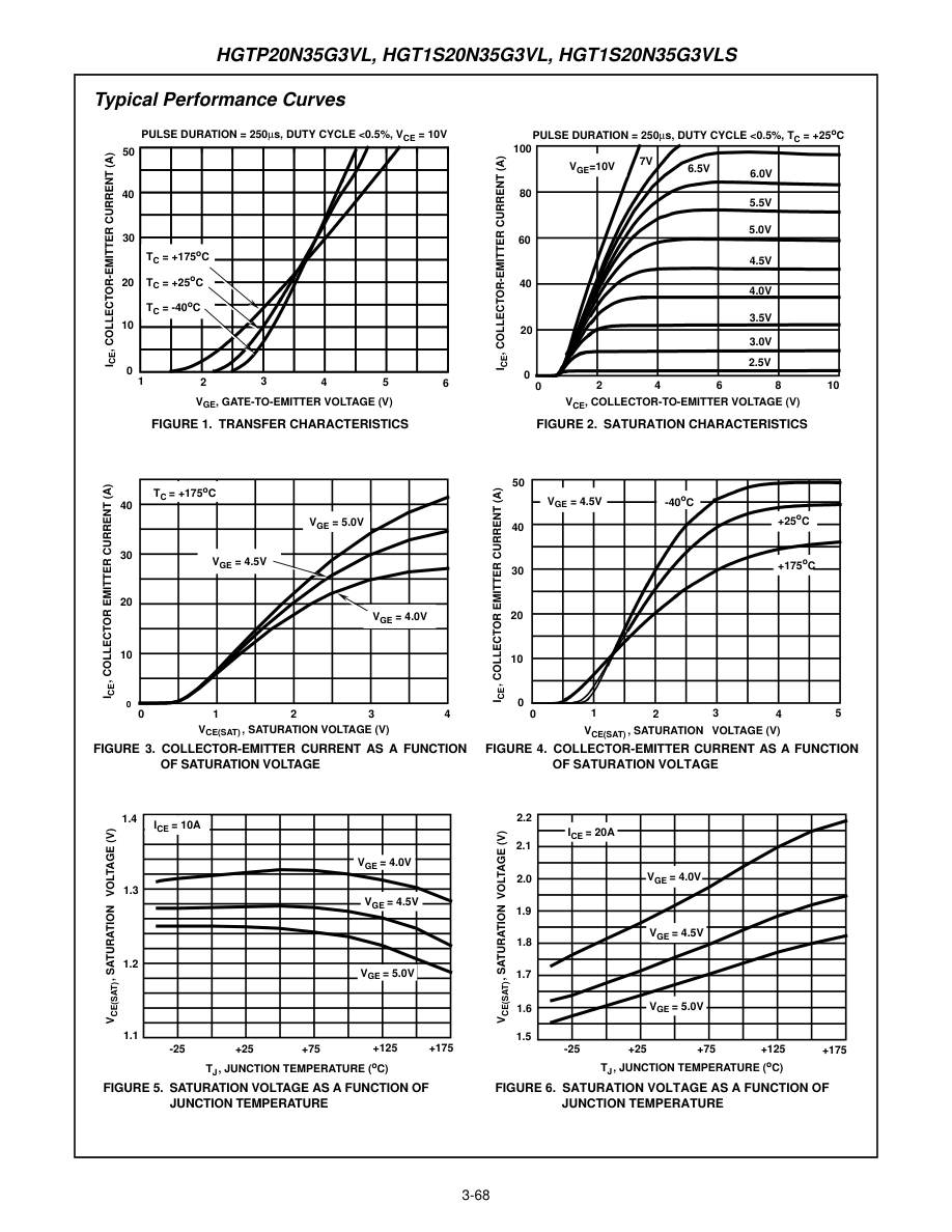
Page 4
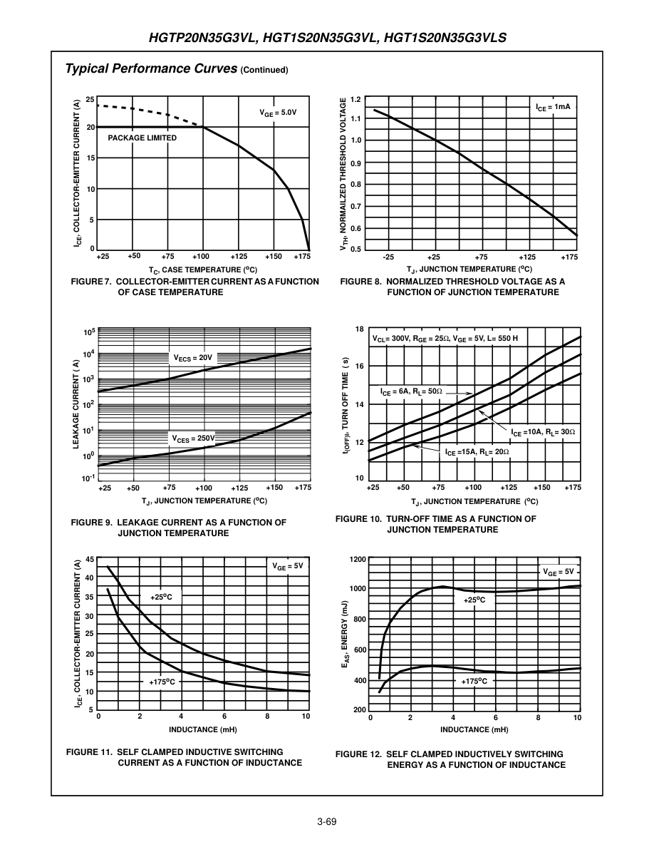
Page 5
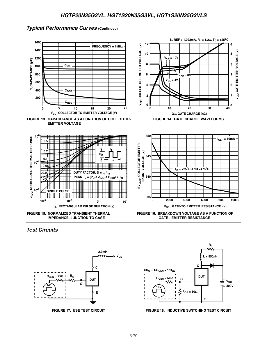
Page 6
All Intersil semiconductor products are manufactured, assembled and tested under ISO9000 quality systems certification. Intersil semiconductor products are sold by description only. Intersil Corporation reserves the right to make changes in circuit design and/or specifications at any time without notice. Accordingly, the reader is cautioned to verify that data sheets are current before placing orders. Information furnished by Intersil is believed to be accurate and reliable. However, no responsibility is assumed by Intersil or its subsidiaries for its use; nor for any infringements of patents or other rights of third parties which may result from its use. No license is granted by implication or otherwise under any patent or patent rights of Intersil or its subsidiaries.
For information regarding Intersil Corporation and its products, see web site www.intersil.com
Sales Office Headquarters
NORTH AMERICA
EUROPE
Intersil Corporation
Intersil SA
P. O. Box 883, Mail Stop 53-204
Mercure Center
Melbourne, FL 32902
100, Rue de la Fusee
TEL: (321) 724-7000
1130 Brussels, Belgium
FAX: (321) 724-7240
TEL: (32) 2.724.2111 FAX: (32) 2.724.22.05
3-71
ASIA
Intersil (Taiwan) Ltd. 7F-6, No. 101 Fu Hsing North Road Taipei, Taiwan Republic of China TEL: (886) 2 2716 9310 FAX: (886) 2 2715 3029
Spec Number