

 Download PDF
DATASHEET SEARCH SITE
Document overview
- PDF pages: 4
Technical content
Page 1
Metal Package PMT with Gate Function
Photosensor Modules H11526 Series
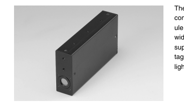
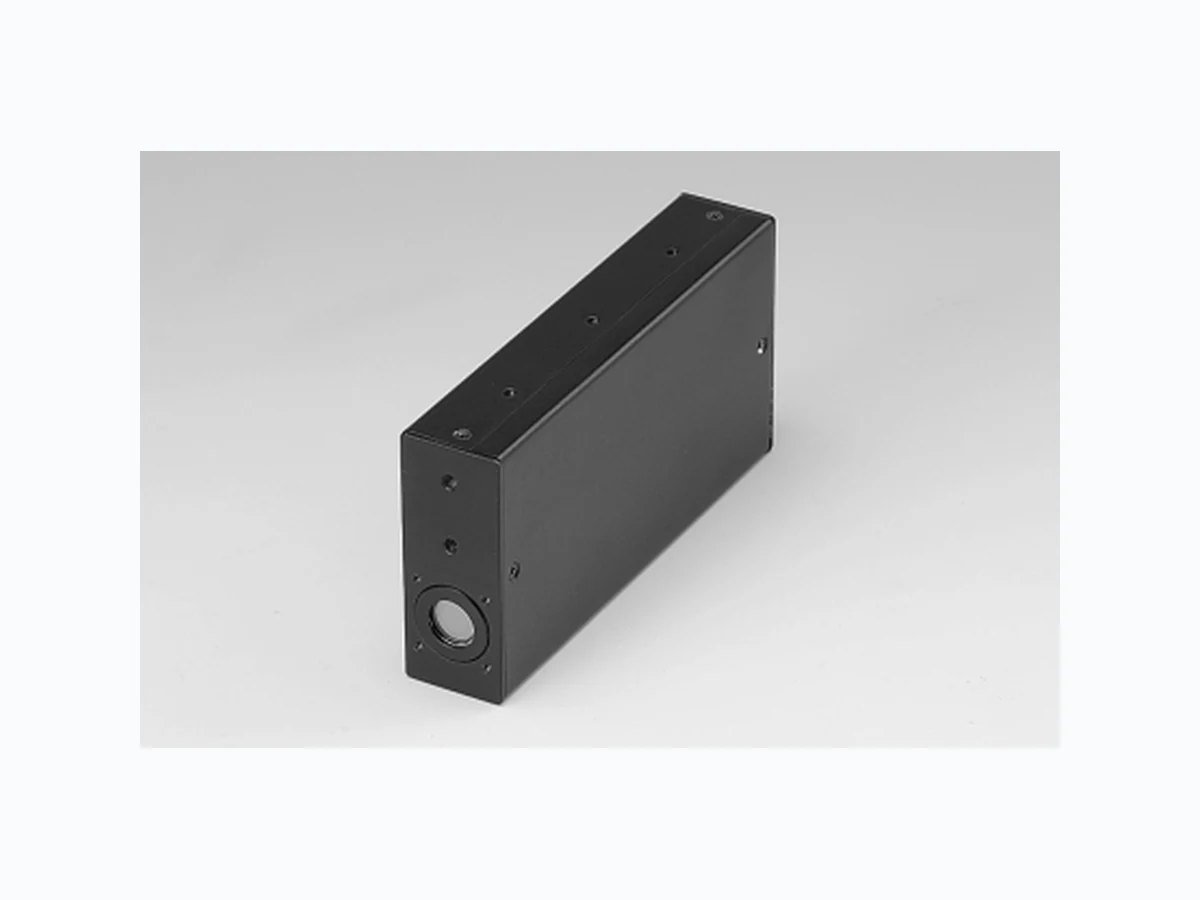
The H11526 series is a photosensor module that allows gate operation. The combination of built-in metal package PMT and gate circuit makes this module compact yet still provides excellent characteristics: 100 ns minimum gate width, 10 kHz repetition rate. This module also contains a high-voltage power supply so that PMT gain can be varied by simply adjusting the control voltage. The internal protection monitor issues an error signal if high-intensity light enters the module.
Product Variations
| Parameter | Spectral Response | Features |
|---|---|---|
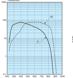
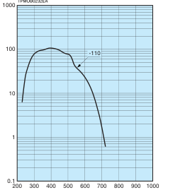
| H11526-110-NN / H11526-110-NF | 230 nm to 700 nm | Super bialkali photocathode, High sensitivity in visible range |
| H11526-01-NN / H11526-01-NF | 230 nm to 870 nm | For UV to near IR range |
| H11526-20-NN / H11526-20-NF | 230 nm to 920 nm | Extended red multialkali photocathode with enhanced sensitivity |
Gate Mode NN: Normally ON NF: Normally OFF This product can't be used at vacuum environment or reduced pressure environment.
Specifications
(at +25 °C)
| Parameter | H11526 Series | Unit | |||
|---|---|---|---|---|---|
| Suffix | -110-NN / -01-NN / -20-NN | -110-NF / -01-NF / -20-NF | — | ||
| Gate Mode | Mode | Normally ON | Normally OFF | — | |
| Gate Width (FWHM) | 100 ns to DC | — | |||
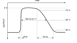
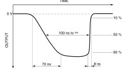
| Rise Time | 8 | 70 | ns | ||
| Fall Time | 70 | 8 | ns | ||
| Repetition Rate | Max. | 10 | kHz | ||
| Switching Ratio | 106 | — | |||
| Switching Noise *1 | Max. | 30 | mV | ||
| Delay Time | Max. | 80 | 180 | ns | |
| Gate Jitter | Max. | 1 | ns | ||
| Gate Signal Input | Level | C-MOS (High level: +3.5 V to +5 V) | — | ||
| Input Impedance | 10 | kΩ | |||
| Pulse Width | 20 ns to DC | — | |||
\*1: Load resistance = 50 Ω (peak to peak)
Page 2
Photosensor Module with Gate Function
| Parameter | H11526 Series | Unit | |||||
|---|---|---|---|---|---|---|---|
| Suffix | -110-NN / -110-NF | -01-NN / -01-NF | -20-NN / -20-NF | — | |||
| Input Voltage | +14.5 to +15.5 | V | |||||
| Max. Input Voltage | +16 | V | |||||
| Max. Input Current | 60 | mA | |||||
| Max. Surge Current | 300 | mA | |||||
| Max. Output Signal Current | 100 | µA | |||||
| Pulse Linearity (±5 % Deviation) *2 | 30 | mA | |||||
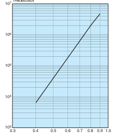
| Max. Control Voltage | +0.9 (Input Impedance 10 kΩ) | V | |||||
| Recommended Control Voltage Adjustment Range | +0.4 to +0.9 (Input Impedance 10 kΩ) | V | |||||
| Effective Area | 8 | mm | |||||
| Peak Sensitivity Wavelength | 400 | 400 | 630 | nm | |||
| Cathode | Luminous Sensitivity | Min. | 80 | 100 | 350 | µA/lm | |
| Typ. | 105 | 200 | 500 | ||||
| Blue Sensitivity Index (CS 5-58) | Typ. | 13.5 | — | — | — | ||
| Red / White Ratio | Typ. | — | 0.2 | 0.45 | — | ||
| Radiant Sensitivity *3 | Typ. | 110 | 77 | 78 | mA/W | ||
| Anode | Luminous Sensitivity *2 | Min. | 80 | 100 | 350 | A/lm | |
| Typ. | 210 | 400 | 1000 | ||||
| Radiant Sensitivity *2 *3 | Typ. | 2.2 × 10⁵ | 1.5 × 10⁵ | 1.5 × 10⁵ | A/W | ||
| Dark Current *2 *4 | Typ. | 1 | 1 | 10 | nA | ||
| Max. | 10 | 10 | 100 | ||||
| Time Response *2 | Rise Time | Typ. | 0.57 | ns | |||
| Transit Time | Typ. | 2.7 | ns | ||||
| T.T.S. | Typ. | 0.2 | ns | ||||
| Ripple Noise *2 *5 (peak to peak) | Max. | 5 | mV | ||||
| Settling Time *6 | Max. | 2 | s | ||||
| Operating Ambient Temperature *7 | +5 to +45 | °C | |||||
| Storage Temperature *7 | -20 to +50 | °C | |||||
| Weight | 105 | g | |||||
\*2: Control voltage = +0.8 V \*3: Measured at the peak sensitivity wavelength \*4: After 30 minutes storage in darkness. \*5: Cable RG-174/U, Cable length 450 mm, Load resistance = 1 MΩ, Load capacitance = 22 pF \*6: The time required for the output to reach a stable level following a change in the control voltage from +0.8 V to +0.4 V. \*7: No condensation
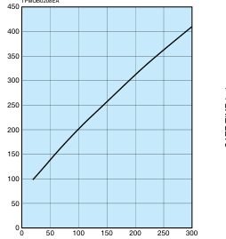
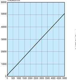
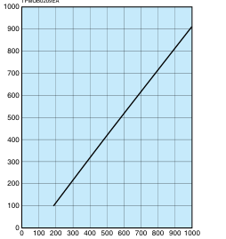
Characteristics (Cathode radiant sensitivity, Gain)
WAVELENGTH (nm)
CONTROL VOLTAGE (V)
WAVELENGTH (nm)
Page 3
Metal Package PMT with Gate Function
Gate Timing Chart
Normally ON Type
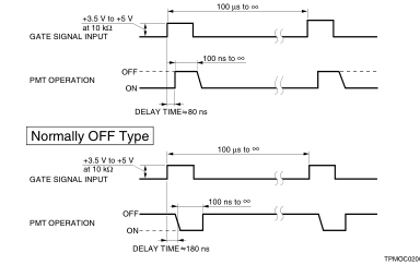
Gate Time Characteristics
Normally ON Type
Normally ON Type closeup
Output Examples
Normally ON Type
TIME
TPMOB0205EA
Normally OFF Type
TIME
TPMOB0206EA
Normally OFF Type
TPMOB0207EA
TPMOB0208EA
TPMOB0209EA
INPUT PULSE WIDTH (ns)
INPUT PULSE WIDTH (ns)
INPUT PULSE WIDTH (ns)
Block Diagram
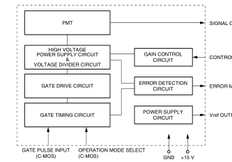
SIGNAL OUTPUT: OUTPUT CURRENT (SMA)
CONTROL VOLTAGE INPUT
ERROR MONITOR
Vref OUTPUT (+1.2 V)
POWER INPUT
TPMOC0201EB
Page 4
Photosensor Module with Gate Function H11526 Series
Sensitivity Adjustment Method
Voltage Programming
SIGNAL GATE PULSE
POWER SUPPLY
OUTPUT INPUT (C-MOS)
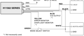
TPMOC0236EA
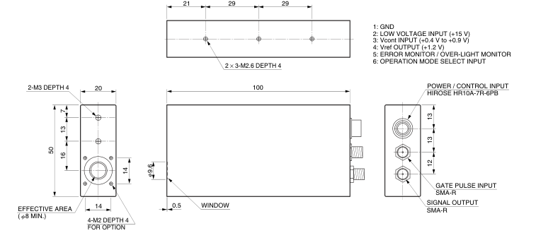
Dimensional Outlines (Unit: mm)
Resistance Programming
SIGNAL GATE PULSE
POWER SUPPLY
OUTPUT INPUT (C-MOS)
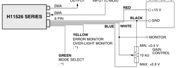
POTENTIOMETER
\*1: Not necessarily used.
(RECOMMENDED: 10 kΩ)
When using a potentiometer, adjust sensitivity while monitoring
TPMOC0237EA
the control voltage so it does not exceed +0.9 V.
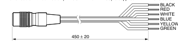
Power cable with connector (HIROSE HR10A-7P-6S) is supplied with H11526 series
: GND : LOW VOLTAGE INPUT (+15 V) : Vcont INPUT (+0.4 V to +0.9 V) : Vref OUTPUT (+1.2 V) : ERROR MONITOR / OVER-LIGHT MONITOR : OPERATION MODE SELECT INPUT
TPMOA0071EA