


 Download PDF
GF9320 GENNUM
Document overview
- PDF pages: 60
Technical content
Page 1

Features
- broadcast quality 10 / 8-bit 24-tap poly-phase horizontal and vertical scalar for HDTV / SDTV video images
- high performance 2D scaling processor with separate control of horizontal and vertical scaling factors and pan positions
- support for arbitrary video formats up to 2048 by 2048
- support for multiplexed and non-multiplexed Y/C video
- flexible 4:2:2 or 4:4:4 YCbCr or RGB output
- field merge / separation can be inserted / removed from progressive images using interlaced I/O
- double banked control registers for 'on-the-fly' dynamic effects
- external 3:2 / 2:2 pull-down insertion and extraction
- programmable output matrix with 6dB gain range
- film rate features include 1080p24 and 1080PsF support
- fully programmable colour background generator
- flexible F,V,H output and TRS insertion
- seamless interface to GF9330 de-interlacer
- seamless interface to common SDRAM
- user configuration through dedicated serial interface
- 3.3V supply
Description
The GF9320 Scaling Processor offers 10 / 8-bit broadcast quality scaling of video images up to 2048 by 2048 pixels. The GF9320 supports arbitrary display modes to fit custom applications. Dynamic zoom and pan effects allow for a variety of aspect ratio conversion
choices while a programmable colour background generator can be customized to appropriately match the image content. A fully programmable and flexible output matrix allows for colour difference over-sampling, gain and hue controls as well as YCbCr to RGB conversions to power nearly any display device on the market.
The GF9320 also includes a vertical interpolation filter to perform stand alone cost-sensitive de-interlacing. Broadcast quality de-interlacing is offered through a seamless interface to the GF9330 and GF9331 devices.
Applications
- HDTV Up / Down Converters
- Production Equipment
- Video Walls
- Projection Systems
- Plasma Displays
- LCD TVs
- Home Theatre Systems
- HD DVD Players
Ordering Information
Part Number
Package
Temp. Range
GF9320-CBW
352 pin TBGA
0oC to 70oC
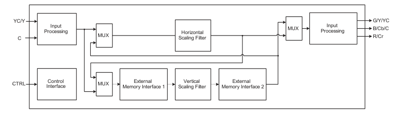
Block Diagram
1 of 60
www.gennum.com
Page 2
Contents
Features ........................................................................................................................1 Description ....................................................................................................................1 Applications...................................................................................................................1 Ordering Information .....................................................................................................1 1. Pin Description ..........................................................................................................3 2. Electrical Characteristics...........................................................................................7
- Detailed Device Description ....................................................................................11 3.1 Device Overview ...........................................................................................11 3.2 Serial Interface Control .................................................................................12 3.3 Input Processing ...........................................................................................21 3.4 Scaling Processor .........................................................................................22 3.5 SDRAM Memory Interface ............................................................................34
3.6 Output Processor ..........................................................................................57 3.7 Output Timing Control ...................................................................................58 4. Package Dimensions ..............................................................................................59 5. Revision History ......................................................................................................60
2 of 60
Page 3
1. Pin Description
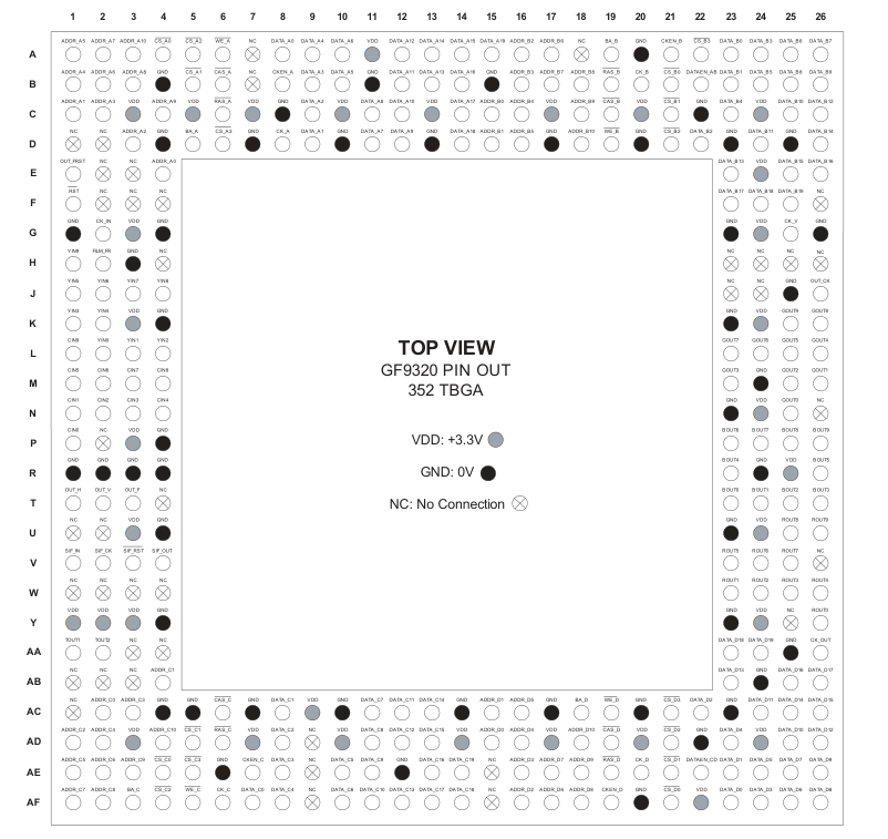
Figure 1-1: GF9320 Pin Out
3 of 60
Page 4
Table 1-1: Pin Descriptions
Symbol
Pin Grid
Type Description
10-bit multiplexed signed luminance / signed offset colour difference data
YIN[9:0]
H1, J4, J3, J2, J1, K2, K1,
I
L4, L3, L2
input. Note that either input must include TRS words.
10-bit signed offset colour difference data input.
CIN[9:0]
L1, M4, M3, M2, M1, N4,
I
N3, N2, N1, P1
Note that theinput must include TRS words.
CK_IN
G2
I Input clock. Note that it is equal Y data rate for separate Y and C inputs, and is equal to 2x Y data rate for multiplexed YC input.
Vertical processing clock.
CK_V
G25
I Note that it is usually the higher of CK_IN or CK_OUT.
CK_OUT
AA26
I Output clock.
Input film sequence reset.
FILM_FR
H2
I
Output frame reset.
OUT_FRST
E1
I
10 / 8-bit unsigned green data output OR
GOUT[9:0]
K25, K26, L23, L24, L25,
O
L26, M23, M25, M26, N25
10 / 8-bit unsigned luminance data output OR 10 / 8-bit multiplexed signed luminance / signed offset colour difference data output.
10 / 8-bit unsigned blue data output OR
BOUT[9:0]
P26, P25, P24, P23, R26,
O
R23, T26, T25, T24, T23
10 / 8-bit signed offset (B-Y) data output OR 10/8-bit multiplexed signed offset colour difference data output.
10 / 8-bit unsigned red data output OR O
ROUT[9:0]
U26, U25, V25, V24, V23, W26, W25, W24, W23,
10 / 8-bit signed offset (R-Y) data output.
Y26
Output clock timed to clock output data.
OUT_CK
J26
O
Output format frame / field signal.
OUT_F
T3
O Note that the output is 3 clocks in advance of output video data.
Output format vertical signal.
OUT_V
T2
O Note that the output is 3 clocks in advance of output video data.
Output format horizontal signal.
OUT_H
T1
O Note that the output is 3 clocks in advance of output video data.
Serial interface control data out.
SIF_OUT
V4
O
Serial interface control data in.
SIF_IN
V1
I
Serial interface clock.
SIF_CK
V2
I
Serial interface reset.
SIF_RST
V3
I
Power-on reset.
RST
F1
I
Data bus for memory array A. I/O
DATA_A[19:0]
A15, D14, C14, B14, A14, A13, B13, A12, B12, C12, D12, C11, D11, A10, B10, A9, B9, C9, D9, A8
4 of 60
Page 5
Table 1-1: Pin Descriptions (Continued)
Symbol
Pin Grid
Type Description
Data bus for memory array B. I/O
DATA_B[19:0]
F25, F24, F23, E26, E25, D26, E23, C26, D24, C25, B26, B25, A26, A25, B24, C23, A24, D22, B23, A23
Data bus for memory array C. I/O
DATA_C[19:0]
AE14, AF14, AF13, AE13, AD13, AC13, AF12, AD12, AC12, AF11, AE11, AD11, AC11, AF10, AE10, AF8, AE8, AD8, AC8, AF7
Data bus for memory array D. I/O
DATA_D[19:0]
AA24, AA23, AB26, AB25, AC26, AC25, AB23, AD26, AC24, AD25, AE26, AF26, AE25, AF25, AE24, AD23, AF24, AC22, AE23, AF23
Address bus for memory array A.
ADDR_A[10:0]
A3, C4, B3, A2, B2, A1,
O
B1, C2, D3, C1, E4
SDRAM bank select for memory array A.
BA_A
D5
O
Address bus for memory array B. O
ADDR_B[10:0]
D18, C18, B18, B17, A17, D16, C16, B16, A16, D15, C15
SDRAM bank select pin for memory array B.
BA_B
A19
O
Address bus for memory array C. O
ADDR_C[10:0]
AD4, AE3, AF2, AF1, AE2, AE1, AD2, AC3, AD1, AB4, AC2
SDRAM bank select pin for memory array C.
BA_C
AF3
O
Address bus for memory array D. O
ADDR_D[10:0]
AD18, AE18, AF18, AE17, AF17, AC16, AD16, AE16, AF16, AC15, AD15
SDRAM bank select pin for memory array D.
BA_D
AC18
O
Chip select for memory array A.
CS_A[3:0]
D6, A5, B5, A4
O
Chip select for memory array B.
CS_B[3:0]
A22, D21, C21, B21
O
Chip select for memory array C.
CS_C[3:0]
AE5, AF4, AD5, AE4
O
Chip select for memory array D.
CS_D[3:0]
AC21, AD21, AE21, AF21
O
Row address strobe for memory array A.
RAS_A
C6
O
Row address strobe for memory array B.
RAS_B
B19
O
Row address strobe for memory array C.
RAS_C
AD6
O
Row address strobe for memory array D.
RAS_D
AE19
O
Column address strobe for memory array A.
CAS_A
B6
O
Column address strobe for memory array B.
CAS_B
C19
O
Column address strobe for memory array C.
CAS_C
AC6
O
5 of 60
Page 6
Table 1-1: Pin Descriptions (Continued)
Symbol
Pin Grid
Type Description
Column address strobe for memory array D.
AD19
O
CAS_D
Write enable for memory array A.
WE_A
A6
O
Write enable for memory array B.
WE_B
D19
O
Write enable for memory array C.
WE_C
AF5
O
Write enable for memory array D.
WE_D
AC19
O
Clock for memory array A.
CK_A
D8
O
Clock for memory array B.
CK_B
B20
O
Clock for memory array C.
CK_C
AF6
O
Clock for memory array D.
CK_D
AE20
O
Clock enable for memory array A.
CKEN_A
B8
O
Clock enable for memory array B.
CKEN_B
A21
O
Clock enable for memory array C.
CKEN_C
AE7
O
Clock enable for memory array D.
CKEN_D
AF19
O
Data enable for memory arrays A and B.
DATAEN_AB
B22
O
Data enable for memory arrays C and D.
DATAEN_CD
AE22
O
I 3.3V supply.
VDD
K3, C10, A11, P3, C13, U3, C17, Y3, C20, AD3, G3, AD7, AC9, AD10, AD14, AD17, C24, AD20, AF22, AD24, E24, Y24, G24, K24, C5, N24, C3, U24, R25, C7, Y1, Y2
I Device ground.
GND
R24, U23, N23, K23, G26, G23, Y23, D25, AC20, AF20, AC17, D23, AC14, AC10, AC7, AC5, AC4, D20, A20, Y4, D17, B15, U4, D13, P4, B11, D10, K4, D7, G4, B4, D4, AC23, C8, H3, J25, AE6, C22, AE12, M24, AD22, G1, AB24, AA25, R1, R2, R3, R4
No connection.
NC
H26, W2, W3, J23, W4, T4, U1, U2, J24, A7, A18, AA3, AA4, W1, AB1, AB2, F26, AC1, AB3, N26, Y25, F2, V26, F3, P2, B7, D2, AD9, E3, H24, AE9, D1, AF9, E2, AE15, AF15, F4, H23, H25, H4, AA1, AA2
6 of 60
Page 7
2. Electrical Characteristics
Table 2-1: Absolute Maximum Ratings
Parameter
Symbol
Conditions
Rated Value
Units
Power Supply Voltage
VDD
-0.5 to +4.6
V
VI < VDD + 0.5 V
-0.5 to +4.6
V
Input Voltage
VI
VO < VDD + 0.5 V
Output Voltage
VO
-0.5 to +4.6
V
40
mA
Output Current
IO
Operating Temperature
TA
0 to +70
oC
Storage Temperature
TSTG
-65 to +150
oC
Table 2-2: Recommend Operating Conditions
Parameter
Symbol
Conditions
Min.
Typ.
Max.
Units
Power Supply Voltage
VDD
3.0
3.3
3.6
V
High-Level Input Voltage
VIH
TTL Interface
2.0
- VDD
V
TTL Interface
0.0
- 0.8
V
Low-Level Input Voltage
VIL
Positive Trigger Voltage
VP
1.5
- 2.7
V
0.6
- 1.4
V
Negative Trigger Voltage
VN
Hysteresis Voltage
VH
1.1
- 1.5
V
Normal Input
0
- 200
ns
Input Rise Time
tri
Normal Input
0
- 200
ns
Input Fall Time
tfi
7 of 60
Page 8
Table 2-3: DC Characteristics

Static Current Consumption
IDDS
Input Leakage Current
II
Low-Level Output Current
IOL
High-Level Output Current
IOH
Low-Level Output Voltage
VOL
High-Level Output Voltage
VOH
Off-State Output Current
IOZ
Output Short-Circuit Current
IOS
Table 2-4: Capacitance
VI = VDD or GND
10
200
µA
VI = VDD or GND
±10
µA
±10-4
VOL = 0.4V
12.0
-
- mA
VOH = 2.4V
-2.0
-
- mA
IOL = 0 mA
-
- 0.1
V
IOH = 0 mA
VDD - 0.1
-
-
V
VO = VDD or GND
-
- ±10
µA
VO = GND
-
- -250
mA

Input Capacitance
CI
4.0
- 6.4
pF
Output Capacitance
CO
4.0
- 6.0
pF
4.0
- 6.0
pF
I/O Capacitance
CIO
Table 2-5: Operating Current

-
- 910
mA
Operating Current
ICC
CK_IN @ 90MHz CK_OUT @ 90MHz CK_V @ 88MHz
8 of 60
Page 9
Table 2-6: AC Characteristics - Setup & Hold Times

YIN[9:0]
2
-
1
-
CK_IN
ns
CIN[9:0]
2
-
1
-
CK_IN
ns
FILM_FR
-
-
2
-
CK_IN
ns
SIF_IN
1
-
2
-
SIF_CK
ns
SIF_RST
1
-
2
-
SIF_CK
ns
OUT_FRST
1
-
2
-
CK_OUT
ns
DATA_A
2
-
0
-
CK_A
ns
DATA_B
2
-
0
-
CK_B
ns
DATA_C
2
-
0
-
CK_C
ns
DATA_D
2
-
0
-
CK_D
ns
Table 2-7: AC Characteristics - Pulse Signal
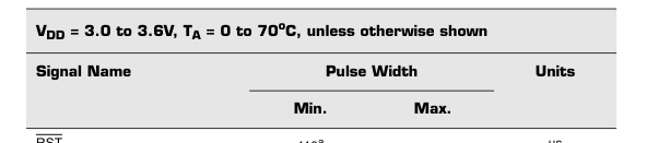
RST
µs
110a
a.The minimum pulse width is for 64Mb SDRAMs. If 16Mb is used them 10µs width can be used.
9 of 60
Page 10
Table 2-8: Output Signal Timing Specifications

OUT_CK
1.81
3.97
CK_OUT
GOUT[9:0]
0.15
3
OUT_CK
BOUT[9:0]
0.15
3
OUT_CK
ROUT[9:0]
0.15
3
OUT_CK
ADDR_A, RAS_A, CAS_A, WE_A, CKEN_A, DATA_A
1.25
6
CK_A
ADDR_B, RAS_B, CAS_B, WE_B, CKEN_B, DATA_B
1.25
6
CK_B
ADDR_C, RAS_C, CAS_C, WE_C, CKEN_C, DATA_C
1.25
6
CK_C
ADDR_D, RAS_D, CAS_D, WE_D, CKEN_D, DATA_D
1.25
6
CK_D
Table 2-9: Clock Frequency

CK_IN
1
90
CK_V
1
88
CK_OUT
1
90
SIF_CK
-
90
10 of 60
Page 11
3. Detailed Device Description
3.1 Device Overview
A system level block diagram is shown in the “Block Diagram” on page 1.
2D scaling is performed by cascading two 1D-scaling filters.
If the number of horizontal input samples is greater than the number of horizontal output samples (i.e. down sampling), then it is advantageous to perform horizontal resizing first. Otherwise, horizontal resizing is performed last. This minimizes the number of operations required, reduces the intermediate image size and thus lowers the SDRAM requirements.
In addition, the SDRAMs are used for field merge or separation operations to perform simple frame rate conversions (e.g. 30 ↔ 60 and 48 ↔ 60) for film applications. This minimizes the on chip memory required to perform 2D format conversion for low-cost, high-quality format conversion.
The GF9320 has 2 fields / frames of delay depending on the selected operating mode.
Processing is performed simultaneously on 3 fields / frames. Input processing is performed on field / frame N, vertical processing is performed on field / frame (N- 1) and output processing is performed on field / frame (N-2).
The input processor decodes the input TRS to determine input video timing information. An area of the input video is selected according to the downloaded parameters. The input video is resized horizontally if down sampling is indicated.
The video is passed to picture memory control #1 and stored in SDRAM. Field / frame (N-1) is read out of picture memory #1, processed vertically, and stored in picture memory #2. To process the video vertically the read address to picture memory #1 transposes the video data while the write address to picture memory #2 transposes the video data back. This transpose operation allows the vertical processing to be done as rows instead of columns.
Field / frame (N-2) is read out of picture memory #2 and resized horizontally if up sampling is indicated.
The flexible output processor can be selected to perform 4:2:2 to 4:4:4 colour difference over sampling, YCbCr to RGB conversion, colour background insertion and output TRS insertion.
11 of 60
Page 12
3.2 Serial Interface Control
The serial interface download control parameters are grouped into 5 sets as given in Table 3-1: Serial Interface Download Groups. All parameters may be
downloaded at once or each set can be downloaded individually. This grouping allows for quick downloading of dynamic parameters (e.g. zoom, pan, gain, etc.)
and only requires that the static parameters be downloaded once. Details of individual control parameters are provided in Table 3-2: Serial Interface Download Parameters.
Table 3-1: Serial Interface Download Groups
Name
CMD ID
No. of
Number of
Bytes
Bits
0
147
1176
All Parametersa
00000000b
11 7 + 14 + 66
I/O Format
1
Parameters
+ 1 (fill) = 88
00100000b
Scaling
2
19 149 + 3 (fill) = 152
Parameters
01000000b
20 157 + 3 (fill) = 160
Dynamic Output
3
Parameters
01100000b
Horizontal Filter
4
43 344 + 0 (fill) = 344
Coefficients
10000000b
54 428 + 4 (fill) = 432
Vertical Filter
5
Coefficients
10100000b
a. The GF9320 download parameters are grouped into 5 sets.
Description
Word
A download of all parameters.
AP[1175:0]
Input and static output parameters.
IO[87:0]
These parameters tend to remain fixed once the input and output format is selected.
Resizing parameters.
RS[151:0]
These parameters change with zoom, pan, and crop controls.
Dynamic output parameters.
OD[159:0]
These parameters change with gain, H position, line advance, etc...
Horizontal filter.
HF[343:0]
Vertical filter.
VF[431:0]
b.Each group will be extended with zeros to make an integer number of bytes. In each group the LSB is sent first. So, for instance, the I/ O format parameter group sends 1 zero followed by the PROC_8_BITS bit followed by the OUT_8_BITS bit. A download of all parameters (CMD ID = 0) sends the word: AP[1175:0] = IO[87:0] | RS[151:0] | OD[159:0] | HF[343:0] | VF[431:0] where "|" represents concatenation. As with all other words the LSB of AP[1175:0] is sent first. The CMD_ID word is listed above in binary form from MSB to LSB. As with all other words the CMD_ID is sent LSB first. For example, a download of the dynamic output parameters (CMD_ID=3) sends 5 zeros fol-
lowed by 2 ones followed by 1 zero followed by OD0 followed by OD1 followed by OD2....OD159. Note that all CMD_IDs have 5 zeros as the 5 least significant bits so that each download command starts with 5 zeros.
12 of 60
Page 13
Table 3-2: Serial Interface Download Parameters
Parameter Name
No. Of
Description
Bits
I/O Format Parameters
88 Total
Input Format Parameters
7 Sub-total
IN_PROGRESSIVE
1 Indicates that the input is progressive. 0 - Interlaced 1 - Progressive
IN_TOP_ACT_FLD
1 Used for interlaced formats only. Indicates which field contains the first active line in a frame. (i.e. which field is on top) 0 - Field 0 is on top 1 - Field 1 is on top
IN_TOP_ACT_LONGER
1 Used for interlaced formats only. Indicates if the top field is one line longer than the bottom field. 0 - Top and Bottom fields contain the same number of active lines 1 - Top field has one more active line
IN_YC_MUXED
1 Indicates if the input bus is one 10-bit bus for muxed Y&C data. 0 - Two 10-bit buses for Y and CbCr 1 - Y & C Muxed data on a 10-bit bus
IN_FILM_RATE
2 Input film frame rate. Used for film inputs only. 00 - Input is from film with 3:2 pull-down 01 - Input is from film with 2:2 pull-down 10 - Input is at film rate (24/25 Hz) 11 - Not from film
IN_REFR_LEFT
1 This indicates a left memory array refresh is required and normally indicates that the input is from film. 0 - No refresh 1 - Refresh
Word
Used By
Time
Position
Frame
IO[87]
Input Control
0
IO[86]
Input Control
0
IO[85]
Input Control
0
IO[84]
Input Control
0
IO[83:82]
Input Control
0
IO[81]
Memory
0
Control
13 of 60
Page 14
Table 3-2: Serial Interface Download Parameters (Continued)
Parameter Name
No. Of
Description
Word
Used By
Time
Bits
Position
Frame
Memory Configuration
14 Sub-total
MEM_CONFIG_LEFT
2 Indicates the number of SDRAMs per
IO[80:79]
Memory
0
array in the left bank excluding chips
Control
needed for LSBs if necessary. (i.e. 8-bit processing) 00 - 4 chips 01 - 3 chips 10 - 2 chips 11 - 1 chip
MODE_16_LEFT
1 Maximum number of left bank SDRAM
IO[78]
Memory
0
memory rows used to store a horizontal
Control
active line. 0 - 8 memory rows 1 - 16 memory rows
MEM_CONFIG_RIGHT
2 Indicates the number of SDRAMs per
IO[77:76]
Memory
0
array in the right bank excluding chips
Control
needed for LSBs if necessary. (i.e. 8 bit processing) 00 - 4 chips 01 - 3 chips 10 - 2 chips 11 - 1 chip
MODE_16_RIGHT
1 Maximum number of right bank
IO[75]
Memory
0
SDRAM memory rows used to store a
Control
horizontal active line. 0 - 8 memory rows 1 - 16 memory rows
IO[74:68]
Memory
0
PIX2READ
7 Number of pixels to be pre-read.
Control
Vertical processing requires prereading samples so that no hits occur while processing a column of data.
OUT_REFR_RIGHT
1 This indicates a right memory array
IO[67]
Memory
0
refresh is required and normally
Control
indicates that the input is from film. 0 - No refresh 1 - Refresh
14 of 60
Page 15
Table 3-2: Serial Interface Download Parameters (Continued)
Parameter Name
No. Of
Description
Word
Used By
Time
Bits
Position
Frame
Static Output Format Parameters 67 Sub-total
OUT_HLEN_TOT
12 The total number of samples per line.
IO[66:55]
Output
0
(e.g. 2200)
Timing
OUT_VLEN_TOT
12 The total number of output lines in a
IO[54:43]
Output
0
frame. (e.g. 1125)
Timing
IO[42:32]
Output
0
OUT_HLEN_ACT
11 The number of active samples per line
Timing
minus 1. (e.g. 1919 implies 1920 active samples)
IO[31:21]
Output
0
OUT_VLEN_ACT
11 The number of active output lines
Timing
minus 1. (e.g. 1079 implies 1080 active lines)
0
OUT_PROGRESSIVE
1 Indicates that the output is progressive.
IO[20]
Output Timing /
0 - Interlaced
Input Control
1 - Progressive
OUT_TOP_ACT_FLD
1 Used for interlaced formats only.
IO[19]
Output
0
Indicates which field contains the first
Timing
active line in a frame. (i.e. which field is on top) 0 - Field 0 is on top 1 - Field 1 is on top
IO[18]
Output
0
OUT_TOP_ACT_LONGER
1 Used for interlaced formats only.
Timing
Indicates if the top field is one line longer than the bottom field. 0 - Both fields have the same number of active lines 1 - Top field has one more active line
OUT_VACT_POS
8 The position of the first active output
IO[17:10]
Output
0
line relative to the start of the frame.
Timing
For interlaced inputs this implies field 0.
IO[9]
Output
0
OUT_FLD_LONGER
1 Used for interlaced formats only.
Timing
Indicates which field is longer. Interlaced formats contain an odd number of lines. So one field contains more lines. 0 - Field 0 is longer 1 - Field 1 is longer
OUT_REF
1 0 - Input TRS
IO[8]
Output
0
Timing
1 - Output Reset pin on GF9320 (OUT_FRST)
15 of 60
Page 16
Table 3-2: Serial Interface Download Parameters (Continued)
Parameter Name
No. Of
Description
Word
Used By
Time
Bits
Position
Frame
0
OUT_FILM_RATE
2 Output film frame rate.
IO[7:6]
Output Timing /
00 - Output has a 3:2 pull-down
Input Control
sequence 01 - Output has a 2:2 pull-down sequence 10 - Output is at a film rate (24/25 Hz) 11 - Output is not to a film rate or sequence
OUT_MODE
2 Indicates output port configuration.
IO[5:4]
Output
0
00 - 4:4:4 GBR Triple output 01 - 4:4:4 YCbCr Triple output 10 - 4:2:2 YCbCr Muxed single output 11 - 4:2:2 YCbCr Muxed dual output
OUT_TRS_ON
1 Indicates if TRS is inserted into the
IO[3]
Output
0
output. 0 - TRS not inserted 1 - TRS inserted
OUT_8_BITS
1 Indicates that the output is rounded to 8
IO[2]
Output
0
bits. 0 - 10-bit output 1 - 8-bit output
PROC_8_BITS
1 Indicates that H&V processing is
IO[1]
Int. Filters
0
rounded to 8-bits. 0 - 10-bit processing (Requires LSB memory) 1 - 8-bit processing
IO_FILL
1 Not used.
IO[0]
16 of 60
Page 17
Table 3-2: Serial Interface Download Parameters (Continued)
Parameter Name
No. Of
Description
Bits
Resizing Parameters
152 Total
H_PROC_FIRST
1 Indicates horizontal processing is performed first. 0 - Horizontal processing last (H_ZOOM_RATIO < 524288) 1 - Horizontal processing first (H_ZOOM_RATIO >= 524288)
H_FLT_DEC
1 Horizontal filter decimate. 0 - Non-decimate mode 1 - Decimate mode
H_ZOOM_RATIO
22 Horizontal zoom ratio.
⋅ IN_HLIVE 524288 ------------------------------------------------- OUT_HLIVE H_FLT_DEC = 0 if ⋅ IN_HLIVE 524288 -------------------------------------------------
⋅ OUT_HLIVE 2 H_FLT_DEC = 1 if
IN_HSTART_PHASE
7 Indicates the starting horizontal phase to be used for resampling.
IN_HSTART
11 Indicates the first sample to be used for resampling.
IN_HSTOP
11 Indicates the last sample to be used for resampling.
OUT_HSTART
11 Indicates the placement of the first output sample with live data. This value must be even.
OUT_HSTOP
11 Indicates the placement of the last output sample with live data. This value must be odd.
V_FLT_DEC
1 Vertical filter decimate. 0 - Non-decimate mode 1 - Decimate mode
Word
Used By
Time
Position
Frame
1
RS[151]
Glue Logic (Mux) / Mem
2
Control
RS[150]
H Control /
1/3
HBL Filter
1/3
RS[149:128]
H Control
1/3
RS[127:121]
H Control
1/3
1
RS[120:110]
Input Timing / H Control /
1/3
Mem Control
2
1
RS[109:99]
Input Timing / H Control /
1/3
Mem Control
2
3
RS[98:88]
Output Timing / H
1/3
Control /
2
Mem Control
3
RS[87:77]
Output Timing / H
1/3
Control /
2
Mem Control
RS[76]
VBL Filter
2
17 of 60
Page 18
Table 3-2: Serial Interface Download Parameters (Continued)
Parameter Name
No. Of
Description
Word
Used By
Time
Bits
Position
Frame
V_ZOOM_RATIO
22 Vertical zoom ratio.
RS[75:54]
V Control
2
⋅ IN_VLIVE 524288 ------------------------------------------------- OUT_VLIVE V_FLT_DEC = 0 if ⋅ IN_VLIVE 524288 -------------------------------------------------
⋅ OUT_VLIVE 2
=
if V_FLT_VLIVE 1
IN_VSTART_PHASE
7 Indicates the starting vertical phase to
RS[53:47]
V Control
2
be used for resampling.
IN_VSTART
11 Indicates the first line to be used for
RS[46:36]
Input Timing
1
resampling.
/ V Control
2
IN_VSTOP
11 Indicates the last line to be used for
RS[35:25]
Input Timing
1
resampling.
/ V Control
2
3
OUT_VSTART
11 Indicates the placement of the first
RS[24:14]
Output
output line with live data.
Timing / V
2
Control
3
OUT_VSTOP
11 Indicates the placement of the last
RS[13:3]
Output
output line with live data.
Timing / V
2
Control
RS_FILL
3 Not used.
RS[2:0]
160 Total
Dynamic Output Parametersa
Matrix Coefficients
117 Sub-total The matrix coefficient format is ±2.10. (i.e. 1 sign bit, 2 integer bits and 10 fractional bits)
G1
13 Matrix coefficient.
OD[159:147]
Output
1
G = G1\*Y + G2\*Cb + G3\*Cr
OD[146:134]
Output
1
G2
13 Matrix coefficient. G = G1\*Y + G2\*Cb + G3\*Cr
OD[133:121]
Output
1
G3
13 Matrix coefficient. G = G1\*Y + G2\*Cb + G3\*Cr
OD[120:108]
Output
1
B1
13 Matrix coefficient. B = B1\*Y + B2\*Cb + B3\*Cr
OD[107:95]
Output
1
B2
13 Matrix coefficient. B = B1\*Y + B2\*Cb + B3\*Cr
OD[94:82]
Output
1
B3
13 Matrix coefficient. B = B1\*Y + B2\*Cb + B3\*Cr
OD[81:69]
Output
1
R1
13 Matrix coefficient. R = R1\*Y + R2\*Cb + R3\*Cr
18 of 60
Page 19
Table 3-2: Serial Interface Download Parameters (Continued)
Parameter Name
No. Of
Description
Bits
R2
13 Matrix coefficient. R = R1\*Y + R2\*Cb + R3\*Cr
R3
13 Matrix coefficient. R = R1\*Y + R2\*Cb + R3\*Cr
Background Colour
24 Sub-total
Y_BKGD
8 Background colour for Y. Unsigned integer.
CB_BKGD
8 Background colour for Cb. Signed integer.
Background colour for Cr.
CR_BKGD
8
Signed integer.
Output Timing
19 Sub-total
LINE_ADV
4 Line advance with respect to input timing.
H_POS
12 Horizontal position with respect to input timing.
OD_FILL
3 Not used.
Filter Coefficients
776 Total
Horizontal Filter
344 Sub-total
H_Y_FLT_COEF
214 Horizontal Y filter coefficients.
HYBANK:
Center coefficient is ±1.10. (i.e. 1 sign
12|12|11|10|10|9|9|9|9|8|8 = 107
bit, 1 integer bit and 10 fractional bits)
2 filters \* (107 bits) = 214
H_C_FLT_COEF
130 Horizontal C filter coefficients.
HCBANK:
Center coefficient is ±1.10. (i.e. 1 sign bit, 1 integer bit and 10 fractional bits)
12|11|9|9|8|8|8 = 65 2 filters \* (65 bits) = 130
Vertical Filter
432 Sub-total
V_Y_FLT_COEF
214 Vertical Y filter coefficients.
HYBANK:
Center coefficient is ±1.10. (i.e. 1 sign
12|12|11|10|10|9|9|9|9|8|8 = 107
bit, 1 integer bit and 10 fractional bits)
2 filters \* (107 bits) = 214
V_C_FLT_COEF
214 Vertical C filter coefficients.
HCBANK:
Center coefficient is ±1.10. (i.e. 1 sign
12|12|11|10|10|9|9|9|9|8|8 = 107
bit, 1 integer bit and 10 fractional bits)
2 filters \* (107 bits) = 214
VYF_FILL
4 Not used.
Word
Used By
Time
Position
Frame
OD[68:56]
Output
1
OD[55:43]
Output
1
OD[42:35]
Output
1
OD[34:27]
Output
1
OD[26:19]
Output
1
OD[18:15]
Output
0a
Timing
OD[14:3]
Output
0a
Timing
OD[2:0]
HY[343:130]
H Y Filter
1
(See footnoteb)
H C Filter
1
HY[129:0] (See footnoteb)
VY[431:218]
V Y Filter
1
(See footnotec)
VY[217:4]
V C Filter
1
(See footnotec)
VY[3:0]
19 of 60
Page 20
a.The resizing parameters, dynamic output parameters, and the filter coefficients are adjustable (dynamic). The I/O Format parameters are static, i.e. once an input and output format is selected the I/O format parameters tend to remain fixed.
b.HORIZONTAL COEFFICIENT DOWNLOAD FORMAT: HF[343:0] = HYBANK1[106:0] | HYBANK0[106:0] | HCBANK1[64:0] | HCBANK0[64:0]
IN NON-DECIMATE MODE (H_FLT_DEC = 0):
HYBANK0 contains the coefficients for a 21-tap symmetric FIR filter and HCBANK0 contains the coefficients for a 13-tap symmetric FIR filter. HYBANK1 and HCBANK1 are not used when H_FLT_DEC is 0 and should contain 0s. HYBANK0[106:0] = HYT0[11:0] | HYT1[11:0] | HYT2[10:0] | HYT3[9:0] | HYT4[9:0] | HYT5[8:0] | HYT6[8:0] | HYT7[8:0] | HYT8[8:0] | HYT9[7:0] | HYT10[7:0] HYBANK1[106:0] = 0 HCBANK0[64:0] = HCT0[11:0] | HCT1[10:0] | HCT2[8:0] | HCT3[8:0] | HCT4[7:0] | HCT5[7:0] | HCT6[7:0] HCBANK1[64:0] = 0
IN DECIMATE MODE (H_FLT_DEC = 1):
HYBANK0 and HYBANK1 contain the coefficients for a 41-tap symmetric decimation filter while HCBANK0 and HCBANK1 contain the coefficients for a 25-tap symmetric decimation filter. BANK0s contain the center tap (tap 0) and all odd taps (e.g. 1, 3, 5....) while the BANK1s contain a zero and all even taps (e.g. 2, 4, 6....). HYBANK0[106:0] = HYT0[11:0] | HYT1[11:0] | HYT3[10:0] | HYT5[9:0] | HYT7[9:0] | HYT9[8:0] | HYT11[8:0] | HYT13[8:0] | HYT15[8:0] | HYT17[7:0] | HYT19[7:0] HYBANK1[106:0] = "000000000000" | HYT2[11:0] | HYT4[10:0] | HYT6[9:0] | HYT8[9:0] | HYT10[8:0] | HYT12[8:0] | HYT14[8:0] | HYT16[8:0] | HYT18[7:0] | HYT20[7:0] HCBANK0[64:0] = HCT0[11:0] | HCT1[10:0] | HCT3[8:0] | HCT5[8:0] | HCT7[7:0] | HCT9[7:0] | HCT11[7:0]
HCBANK1[64:0] = "000000000000" | HCT2[10:0] | HCT4[8:0] | HCT6[8:0] | HCT8[7:0] | HCT10[7:0] | HCT12[7:0] Further information on the horizontal filter coefficients is given in FIR Filter Parameters (3.4.2.2 FIR Filter Parameters).
c.VERTICAL COEFFICIENT DOWNLOAD FORMAT: VF[431:0] = VYBANK1[106:0] | VYBANK0[106:0] | VCBANK1[106:0] | VCBANK0[106:0] | "0000"
IN NON-DECIMATE MODE (V_FLT_DEC = 0):
VYBANK0 and VCBANK0 both contain the coefficients for a 21-tap symmetric FIR filter. VYBANK1 and VCBANK1 are not used when V_FLT_DEC is 0 and should contain 0s. VYBANK0[106:0] = VYT0[11:0] | VYT1[11:0] | VYT2[10:0] | VYT3[9:0] | VYT4[9:0] | VYT5[8:0] | VYT6[8:0] | VYT7[8:0] | VYT8[8:0] | VYT9[7:0] | VYT10[7:0] VYBANK1[106:0] = 0 VCBANK0[106:0] = VCT0[11:0] | VCT1[11:0] | VCT2[10:0] | VCT3[9:0] | VCT4[9:0] | VCT5[8:0] | VCT6[8:0] | VCT7[8:0] | VCT8[8:0] | VCT9[7:0] | VCT10[7:0] VCBANK1[106:0] = 0
IN DECIMATE MODE (V_FLT_DEC = 1):
VYBANK0 and VYBANK1 together contain the coefficients for a 41-tap symmetric decimation filter while VCBANK0 and VCBANK1 together also contain the coefficients for a 41-tap symmetric decimation filter. BANK0s contain the center tap (tap 0) and all odd taps (e.g. 1, 3, 5....19) while the BANK1s contain a zero and all even taps (e.g. 2, 4, 6....20). VYBANK0[106:0] = VYT0[11:0] | VYT1[11:0] | VYT3[10:0] | VYT5[9:0] | VYT7[9:0] | VYT9[8:0] | VYT11[8:0] | VYT13[8:0] | VYT15[8:0] | VYT17[7:0] | VYT19[7:0] VYBANK1[106:0] = "000000000000" | VYT2[11:0] | VYT4[10:0] | VYT6[9:0] | VYT8[9:0] | VYT10[8:0] | VYT12[8:0] | VYT14[8:0] | VYT16[8:0] | VYT18[7:0] | VYT20[7:0]
VCBANK0[106:0] = VCT0[11:0] | VCT1[11:0] | VCT3[10:0] | VCT5[9:0] | VCT7[9:0] | VCT9[8:0] | VCT11[8:0] | VCT13[8:0] | VCT15[8:0] | VCT17[7:0] | VCT19[7:0] VCBANK1[106:0] = "000000000000" | VCT2[11:0] | VCT4[10:0] | VCT6[9:0] | VCT8[9:0] | VCT10[8:0] | VCT12[8:0] | VCT14[8:0] | VCT16[8:0] | VCT18[7:0] | VCT20[7:0]
The GF9320 parameters are downloaded using a 3-pin serial interface. The serial interface consists of a clock, data and a reset as shown in Figure 3-1: Serial
Interface Download Signal Specification. The serial interface reset (SIF_RST) is provided to re-synchronise the download operation in the event that it is interrupted.
20 of 60
Page 21
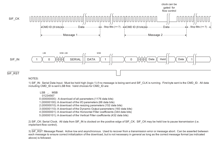
Figure 3-1: Serial Interface Download Signal Specification
3.3 Input Processing
The input processor decodes the input TRS from the incoming video stream. This provides input video timing information to the GF9320. An area of the input video
data is selected for scaling according to the downloaded parameters (i.e. IN_HSTART, IN_HSTOP, IN_VSTART, and IN_VSTOP). This operation is called
the windowing operation. Based on the input field / frame timing and the I/O format parameters a memory enable signal is generated by the input controller. This
signal controls the field / frame switching of the SDRAM memory controller. Also, a frame-reset signal is sent to the output controller for use in internal lock mode
(OUT_REF=0). The frame reset signal and the field / frame switch point is based on input TRS F-bit in interlaced modes (non-film). Otherwise, (i.e. progressive and
all film modes) the frame reset signal and the field / frame switch point is based on one line after input TRS V-bit. Note that in film modes the frame reset signal and
field / frame switch point vary according the input and output frame rates.
21 of 60
Page 22
3.4 Scaling Processor
At the heart of the GF9320 is the scaling processor. It is here where the raw input image selected from the input video is translated into a raw output image of
selected size according to user controlled scaling parameters. As described in 3.1 Device Overview, general 2D scaling is performed by cascading two 1D-scaling
filters. This section describes both the horizontal and vertical scaling filters. A block diagram of the horizontal resizing filter is shown in Figure 3-2: Horizontal Scaling
Filter. A block diagram of the vertical resizing filter is shown Figure 3-3: Vertical Scaling Filter.
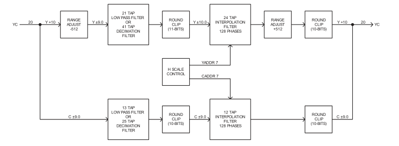
Figure 3-2: Horizontal Scaling Filter
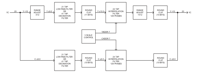
Figure 3-3: Vertical Scaling Filter
22 of 60
Page 23
3.4.1 Scalar Processing
General 1D scaling is performed by cascading an FIR filter with an interpolation filter. The FIR filter is needed to band limit the input signal when the output Nyquist frequency is less than the input Nyquist frequency. The interpolation filter is used to resample the input signal to the new output rate.
3.4.1.1 FIR Filter
The purpose of the FIR filters is to band limit or shape the input signal. Each filter is user programmable, with the coefficients derived depending on the required frequency response. The FIR filter can be used in one of two modes: decimate and non-decimate.
Decimate mode can be used when the output rate is half the input rate. The advantage to using decimate mode is that the number of taps is approximately doubled by using two input clocks to compute one output sample. In non-decimate mode the filter is 21 taps (13 for horizontal colour difference due to the 4:2:2 input video structure). In decimate mode the filter is 41 taps (25 for horizontal colour difference).
Vertically the same modes are available however due to the 4:2:2 sampling structure both luma and colour difference have equal numbers of taps, i.e. 41 taps for decimate and 21 taps for non-decimate.
The filter operation is described by:
= k 10
HYT0_0 HYI n ∑
( ) + ⋅
HYT 2k
k = 1
= ( ) 1024 ⋅ HYO n
k = 10
HYT0_0 HYI n ∑
( ) + ⋅
HYT 2k
k = 1 = k 10 ∑ HYT 2k = k 1
k = 6
∑
–
+ ( )
〈
⋅ HCT0_0 HCI n
HCT 2k
= k 1
= ( ) 1024 ⋅ HCO n
= k 10
∑
+ ( )
〈
⋅ HCT0_0 HCI n
HCT 2k
= k 1 k = 6 ∑ HCT 2k k = 〈 – 1_k〉 ⋅ [
( – k) + ( + k)]
HYI n HYI n
H_FLT_DEC = 0
〈 – 1_k〉 ⋅ [
( – 2k + 1) +
( + 2k – 1)] +
HYI n
HYI n
H_FLT_DEC = 1
– + +
〈 〉 ⋅ [ ( 2k
) ( 2k)]
HYI n HYI n
– + +
1_k〉 ⋅ [ ( k) ( k)]
HCI n HCI n
H_FLT_DEC = 0
–
– + +
+ – +
1_k〉 ⋅ [ ( 2k 1)
( 2k 1)]
HCI n
HCI n
= H_FLT_DEC 1
〈 〉 ⋅ [ ( –
2k) + ( + 2k)]
HCI n
HCI n
23 of 60
Page 24
= k 10
VYT0_0 VYI n ∑ ⋅ ( ) +
VYT 2k
= k 1
= ( ) 1024 ⋅ VYO n
= k 10
VYT0_0 VYI n ∑ ⋅ ( ) +
VYT 2k
k = 1 = k 10 ∑ VYT 2k = k 1
= k 10
∑
+
–
⋅ ( )
〈
VCT0_0 VCI n
VCT 2k
= k 1
= ( ) 1024 ⋅ VCO n
= k 10
VCT0_0 VCI n ∑
( ) + ⋅
VCT 2k
= k 1 k = 10 ∑ VCT 2k k = 1 〈 – 1_k〉 ⋅ [ (
– k) + ( + k)] VYI n VYI n
V_FLT_DEC = 0
〈 – 1_k〉 ⋅ [ (
– 2k + 1) + ( + 2k – 1)] + VYI n
VYI n
= V_FLT_DEC 1
– + +
〈 〉 ⋅ [ ( 2k
) ( 2k)]
VYI n VYI n
– + +
1_k〉 ⋅ [ ( k) ( k)]
VCI n VCI n
V_FLT_DEC = 0
〈 – 1_k〉 ⋅ [
( – 2k + 1) +
( + 2k – 1)] +
VCI n
VCI n
= V_FLT_DEC 1
– + +
〈 〉 ⋅ [ ( 2k
) ( 2k)]
VCI n VCI n
where HYI(n), HCI(n), VYI(n) and VCI(n) are the FIR filter inputs, HYO(n), HCO(n), VYO(n) and VCO(n) are the FIR filter outputs, HYT, HCT, VYT, and VCT are the filter coefficients as given in Table 3-3: Horizontal Filter Coefficients and Table 3-4: Vertical Filter Coefficients, and
1024 is the DC gain of the filter.
In non-decimate mode only one bank of coefficients are used (Bank 0), but in decimate mode both banks of coefficients are used (Bank 0 and Bank 1).
3.4.1.2 Interpolation Filter
After FIR filtering the video data is passed to the interpolation filter where the rate conversion is performed. The interpolation filter is a polyphase filter that allows the output phase to be adjusted every clock cycle. The interpolation filter contains 128 phases (64 phases for horizontal colour difference). The phase selection allows generation of an output anywhere between two inputs with 1/128 input pixel resolution (1/64 for horizontal colour difference). The scaling control unit takes as input the scaling ratio (input / output), and starting phase (starting position of the first output pixel with respect to the input). With these parameters, the scaling
control chooses the correct phasing sequence for the interpolator, determines which input samples should be held and for how long (up sampling), which interpolator outputs should be discarded (down sampling), and generates the new output.
24 of 60
Page 25
3.4.2 Resizing Parameters
In order to understand how to program the GF9320 to perform the necessary conversions an explanation of the window parameters, the zoom parameters and the filter parameters is necessary.
3.4.2.1 Window Parameters
Figure 3-4: Input Window Definition - Progressive through Figure 3-7: Output Window Definition - Interlaced show how the GF9320 places a window over the input and output active video. This window is selected by using offsets from the active video area (HSTART, HSTOP, VSTART, VSTOP). Note that VSTART and VSTOP for interlaced video refers to field based offsets. The windowed portion is referred to as the live video and can cover the entire active video or just a portion of it. The size of the windowed portion is HLIVE by VLIVE pixels where:
HLIVE = HSTOP - HSTART +1
VLIVE = VSTOP - VSTART +1
For interlaced video one field may have one more active line that the other. This means that VLIVE is longer for that field. Also, in interlaced film modes VSTART and VSTOP are still field-based offsets but VLIVE is frame based since the fields are merged and processed as a frame.
The input video window is determined by IN_HSTART, IN_HSTOP, IN_VSTART, and IN_VSTOP. The size of the input windowed portion is IN_HLIVE by IN_VLIVE pixels.
The output video window is determined by OUT_HSTART, OUT_HSTOP, OUT_VSTART, and OUT_VSTOP. The size of the output windowed portion is OUT_HLIVE by OUT_VLIVE pixels.
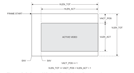
Figure 3-4: Input Window Definition - Progressive
25 of 60
Page 26
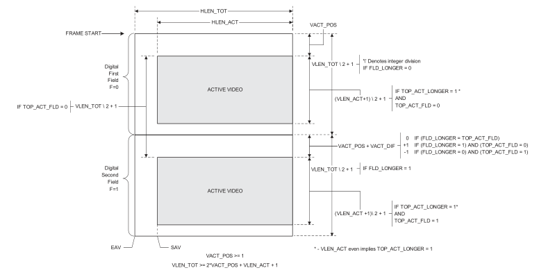
Figure 3-5: Input Window Definition - Interlaced
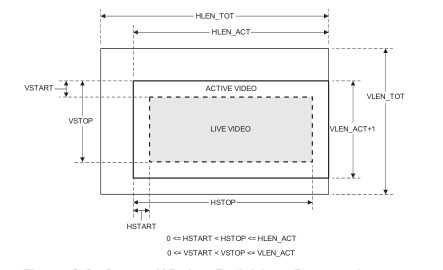
Figure 3-6: Output Window Definition - Progressive
26 of 60
Page 27
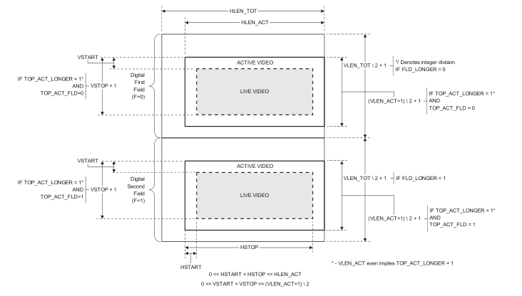
Figure 3-7: Output Window Definition - Interlaced
3.4.2.2 FIR Filter Parameters
The FIR filter shape is programmable by downloading the filter coefficients. The horizontal filter coefficients and download positions are given in Table 3-3:
Horizontal Filter Coefficients. The vertical filter coefficients are given in Table 3-4: Vertical Filter Coefficients. The overall gain of the FIR filter is 1024, but the range
of coefficients is larger to permit implementation of enhancement filters. Note that the coefficients change meaning depending on the filter structure (i.e. if the filter is
in decimate mode or not). The filter structure is determined by the FLT_DEC parameter. If H_FLT_DEC is 1, then the horizontal FIR filter is configured in
decimate mode. If H_FLT_DEC is 0, then the horizontal FIR filter is configured in non-decimate mode. If V_FLT_DEC is 1, then the vertical FIR filter is configured in
decimate mode. If V_FLT_DEC is 0, then the vertical FIR filter is configured in non- decimate mode.
27 of 60
Page 28
Table 3-3: Horizontal Filter Coefficients
Parameter
No. of Bits
Range
Word Position
twelve_zeros
12
[0, 0]
HF[343:332]
HYT2
12
[-2048, 2047]
HF[331:320]
HYT4
11
[-1024, 1023]
HF[319:309]
HYT6
10
[-512, 511]
HF[308:299]
HYT8
10
[-512, 511]
HF[298:289]
HYT10
9
[-256, 255]
HF[288:280]
HYT12
9
[-256, 255]
HF[279:271]
HYT14
9
[-256, 255]
HF[270:262]
HYT16
9
[-256, 255]
HF[261:253]
HYT18
8
[-128, 127]
HF[252:245]
HYT20
8
[-128, 127]
HF[244:237]
HYT0_0
12
[-2048, 2047]
HF[236:225]
HYT1_1
12
[-2048, 2047]
HF[224:213]
HYT3_2
11
[-1024, 1023]
HF[212:202]
HYT5_3
10
[-512, 511]
HF[201:192]
HYT7_4
10
[-512, 511]
HF[191:182]
HYT9_5
9
[-256, 255]
HF[181:173]
HYT11_6
9
[-256, 255]
HF[172:164]
HYT13_7
9
[-256, 255]
HF[163:155]
HYT15_8
9
[-256, 255]
HF[154:146]
HYT17_9
8
[-128, 127]
HF[145:138]
HYT19_10
8
[-128, 127]
HF[137:130]
twelve_zeros
12
[0, 0]
HF[129:118]
HCT2
11
[-1024, 1023]
HF[117:107]
HCT4
9
[-256, 255]
HF[106:98]
HCT6
9
[-256, 255]
HF[97:89]
HCT8
8
[-128, 127]
HF[88:81]
HCT10
8
[-128, 127]
HF[80:73]
HCT12
8
[-128, 127]
HF[72:65]
HCT0_0
12
[-2048, 2047]
HF[64:53]
HCT1_1
11
[-1024, 1023]
HF[52:42]
HCT3_2
9
[-256, 255]
HF[41:33]
28 of 60
Page 29
Table 3-3: Horizontal Filter Coefficients (Continued)
Parameter
No. of Bits
Range
Word Position
HCT5_3
9
[-256, 255]
HF[32:24]
HCT7_4
8
[-128, 127]
HF[23:16]
HCT9_5
8
[-128, 127]
HF[15:8]
HCT11_6
8
[-128, 127]
HF[7:0]
Table 3-4: Vertical Filter Coefficients
Parameter
No. of Bits
Range
Word Position
twelve_zeros
12
[0, 0]
VF[431:420]
VYT2
12
[-2048, 2047]
VF[419:408]
VYT4
11
[-1024, 1023]
VF[407:397]
VYT6
10
[-512, 511]
VF[396:387]
VYT8
10
[-512, 511]
VF[386:377]
VYT10
9
[-256, 255]
VF[376:368]
VYT12
9
[-256, 255]
VF[367:359]
VYT14
9
[-256, 255]
VF[358:350]
VYT16
9
[-256, 255]
VF[349:341]
VYT18
8
[-128, 127]
VF[340:333]
VYT20
8
[-128, 127]
VF[332:325]
VYT0_0
12
[-2048, 2047]
VF[324:313]
VYT1_1
12
[-2048, 2047]
VF[312:301]
VYT3_2
11
[-1024, 1023]
VF[300:290]
VYT5_3
10
[-512, 511]
VF[289:280]
VYT7_4
10
[-512, 511]
VF[279:270]
VYT9_5
9
[-256, 255]
VF[269:261]
VYT11_6
9
[-256, 255]
VF[260:252]
VYT13_7
9
[-256, 255]
VF[251:243]
VYT15_8
9
[-256, 255]
VF[242:234]
VYT17_9
8
[-128, 127]
VF[233:226]
VYT19_10
8
[-128, 127]
VF[225:218]
twelve_zeros
12
[0, 0]
VF[217:206]
VCT2
12
[-2048, 2047]
VF[205:194]
VCT4
11
[-1024, 1023]
VF[193:183]
29 of 60
Page 30
Table 3-4: Vertical Filter Coefficients (Continued)
Parameter
No. of Bits
Range
Word Position
VCT6
10
[-512, 511]
VF[182:173]
VCT8
10
[-512, 511]
VF[172:163]
VCT10
9
[-256, 255]
VF[162:154]
VCT12
9
[-256, 255]
VF[153:145]
VCT14
9
[-256, 255]
VF[144:136]
VCT16
9
[-256, 255]
VF[135:127]
VCT18
8
[-128, 127]
VF[126:119]
VCT20
8
[-128, 127]
VF[118:111]
VCT0_0
12
[-2048, 2047]
VF[110:99]
VCT1_1
12
[-2048, 2047]
VF[98:87]
VCT3_2
11
[-1024, 1023]
VF[86:76]
VCT5_3
10
[-512, 511]
VF[75:66]
VCT7_4
10
[-512, 511]
VF[65:56]
VCT9_5
9
[-256, 255]
VF[55:47]
VCT11_6
9
[-256, 255]
VF[46:38]
VCT13_7
9
[-256, 255]
VF[37:29]
VCT15_8
9
[-256, 255]
VF[28:20]
VCT17_9
8
[-128, 127]
VF[19:12]
VCT19_10
8
[-128, 127]
VF[11:4]
fill
4
[0, 0]
VF[3:0]
3.4.2.3 Zoom Parameters
The zoom parameters (IN_HSTART_PHASE, IN_VSTART_PHASE, H_ZOOM_RATIO,
and V_ZOOM_RATIO) specify the precise conversion from the input live video to the output live video. IN_HSTART_PHASE and IN_VSTART_PHASE allows for
starting the interpolator with sub-pixel accuracy. This allows for maintaining the true center of picture when zooming and panning. The zoom ratio is approximately:
⋅ IN_HLIVE 524288 -------------------------------------------------
H_FLT_DEC = 0
OUT_VLIVE =
H_ZOOM_RATIO
⋅ IN_HLIVE 524288 -------------------------------------------------
=
H_FLT_DEC 1
OUT_HLIVE 2
⋅ ⋅ IN_VLIVE 524288 -------------------------------------------------
=
V_FLT_DEC 0
OUT_VLIVE =
V_ZOOM_RATIO
⋅ IN_VLIVE 524288 -------------------------------------------------
=
V_FLT_DEC 1
OUT_VLIVE 2
⋅
30 of 60
Page 31
The above equations hold only approximately because the zoom ratio must be adjusted to maintain the true center of picture.
When using the GF9320 there is a preventable condition whereby certain memory configurations cause artifacts in the output image. It is dependent upon the vertical parameters of the output video and the number of SDRAMS employed in the right memory bank as follows:
OUT_VLIVE modulo (64 \* N) = (64 \* N) - 3 or (64 \* N) – 1
Where N is the number of memories in each array of the right bank, MEM_CONFIG_RIGHT, and
OUT_VLIVE = OUT_VSTOP – OUT_VSTART + 1
Artifacts can be avoided by monitoring for the condition. When detected, add or subtract one (1) from the OUT_VSTOP value while maintaining the condition:
0 <= OUT_VSTART < OUT_VSTOP
Note that both fields must be checked for this condition when the output is interlaced with one field longer.
3.4.3 Dynamic Zoom and Pan Considerations
The GF9320 is designed to perform frame accurate zooming and panning. Some of the downloaded zoom and pan parameters are used by multiple blocks within the GF9320. These blocks operate on the video data at different time frames. For instance, the input control block operates on the video data on frame / field (N) while the vertical scaling block operates on the video data on frame / field (N-1). Both these blocks need the IN_VSTART parameter. So, the IN_VSTART parameter must be used by the scaling block one field / frame later than the input block. Registering the IN_VSTART parameter on the field / frame boundary before the scaling block uses it does this.
While most dynamic zoom and pan situations are taken care of automatically by the GF9320, some dynamic zoom and pan conditions require special downloading.
3.4.3.1 H_PROC_FIRST Switching
The H_PROC_FIRST download bit is special because it actually changes the configuration of the GF9320. In particular, changing the H_PROC_FIRST bit from 1 to 0 makes the horizontal filter switch from operating on field / frame (N) to operating on field / frame (N-2) and vice versa. Note that changing the H_PROC_FIRST bit from 1 to 0 is changing from down sampling to up sampling. In order to handle this special case smoothly, a 1:1 horizontal zoom factor must be downloaded.
31 of 60
Page 32
The recommended sequence for switching from H_PROC_FIRST equal to 1 to 0 (i.e. down sampling to up sampling) is:
- Keep H_PROC_FIRST equal to 1 and download H_ZOOM_RATIO equal to 524,288 (down sampling).
- Wait at least 2 frames / fields.
- Change H_PROC_FIRST to 0 and download H_ZOOM_RATIO equal to 524,287 (up sampling).
- Change to the desired H_ZOOM_RATIO.
The recommended sequence for switching from H_PROC_FIRST equal to 0 to 1 (i.e. up sampling to down sampling) is:
- Keep H_PROC_FIRST equal to 0 and download a H_ZOOM_RATIO equal to 524,287 (up sampling).
- Change H_PROC_FIRST to 1 and download H_ZOOM_RATIO equal to 524,288 (down sampling).
- Change to the desired H_ZOOM_RATIO.
3.4.3.2 V_FLT_DEC Switching
The vertical filter operates on field / frame (N-1), but the vertical filter coefficients operate on field / frame (N). When the V_FLT_DEC is switched from 0 to 1 or vice versa, the vertical filter coefficients must be delayed by one field / frame so that they operate on the same time frame. This is necessary because the filter coefficients are used differently in decimation mode and a non-decimation filter would be used in decimation mode and vice versa. This would most directly affect the DC gain of the filter that may be perceived as a brightness change in the output video. The horizontal coefficients do not need to be delayed when switching H_FLT_DEC because the horizontal filter and the horizontal coefficients operate
on the same frame / field (N). Even though H_FLT_DEC is switched, down sampling (H_PROC_FIRST=1) is indicated. Delaying the vertical filter coefficients may not be necessary depending on the application.
3.4.3.3 Pseudo Synchronous Film Mode Conversions
This section applies to any film mode conversion when the input frame rate or the output film rate is 3:2 pull-down, but the input rate is not (i.e. 48J60, 24J60). In these cases the zoom and pan update rate is restricted to every other film frame as shown in Figure 3-8: 24/24/60 Download Restrictions and Figure 3-9: 48/24/60 Download Restrictions. This is because the output circuit must be updated on an output field / frame boundary.
32 of 60
Page 33
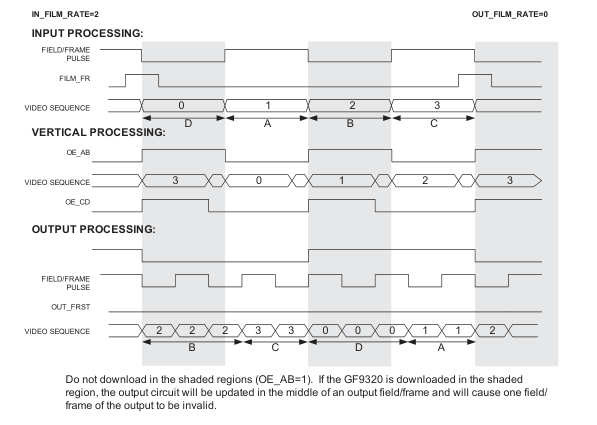
Figure 3-8: 24/24/60 Download Restrictions
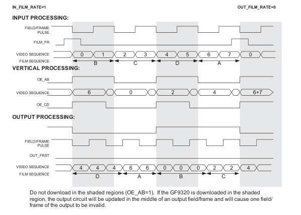
Figure 3-9: 48/24/60 Download Restrictions
33 of 60
Page 34
3.5 SDRAM Memory Interface
3.5.1 Memory Interface Description
To achieve high quality scaling of images in two dimensions, separate processing has to be done in the horizontal and vertical dimensions using one dimensional
filter banks. Hence, the input image has to be transposed before and after vertical processing and uses SDRAMs to achieve real-time transposition of digital video images using high quality filters.
The SDRAM controller within the GF9320 acts as the master controller of the memory arrays. To perform a transpose operation the memory controller writes the
entire image from one field into the image buffer and then reads it out during the next field. Further, during film mode processing, the controller can put two
consecutive image fields together and read them out in the next frame as a single progressive frame. The latter technique is used for processing film material with 3:2
pull-down. We can also separate even and odd fields from a progressive frame to create film material with 3:2 pull-down. The memory organization for transposing
images at high data rates is shown in Figure 3-10: Memory Interface.
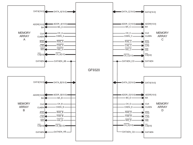
Figure 3-10: Memory Interface
34 of 60
Page 35
The memory organization consists of four arrays of memories communicating with the GF9320. Each array can contain anywhere between one to five SDRAMs based on format conversion mode. Memory array A and B compose the left bank while memory array C and D compose the right bank. To achieve high bandwidth, the memory arrays are arranged in an interleaved fashion. That is, when one field in written into memory array A, the other field will be read out of memory array B. The sequence of read / write operations that takes place in non-film applications is shown in Figure 3-11: Timing Diagram of Data between GF9320 and SDRAMs for non-film Modes.
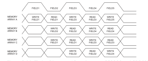
Figure 3-11: Timing Diagram of Data between GF9320 and SDRAMs for nonfilm Modes
The data from an odd field is written into memory array A during Field3. At the same time data from the previous (even) field will be read out as a transposed image from memory array B. The horizontal rows of data read out from memory array B will then be processed (vertical processing) within the GF9320 and written into memo ry array D. Simultaneously, the vertically processed image data from two fields back which was written into memory array C will be read out. When the image is read out from memory array C, it went through another image transposition so that the image is back to its original orientation. Effectively, there is a two field / frame
delay when processing non-film material.
The GF9320 experiences significantly more processing time in the vertical processing section due to the bandwidth limitations of the SDRAMs. For some con versions the processing time might exceed the available time. This condition can be circumvented by either increasing the number of memories in the array or by increasing the processing clock rate.
During vertical processing, the GF9320 pre-reads (number of pixels = PIX2READ) into its internal FIFO, before the beginning of every scan line so that it can supply the pixels from the FIFO into the one-dimensional filter in an uninterrupted way. The number of pixels to be pre-read is chosen based on several I/O parameters so that it is high enough to supply data continuously to the filter but low enough to complete the vertical processing in the available time.
35 of 60
Page 36
The PIX2READ parameter is calculated by:
IN_VLEN_ACT ---------------------------------------------------------- – 2 IN_PROGRESSIVE
( CEIL ----------------------------------------------------------------------------------- ,10) 127
=
+
PIX2READ MIN MAX 8
{
, }
64 × (4 MEM_CONFIG_LEFT) –
Where IN_VLEN_ACT is the total number of active lines per frame,
CEIL(x) is the smallest integer larger than x;
if a ≥ b a ( , ) = MAX a b
if a < b b
if a ≥ b a ( , ) = MAX a b
if a < b b
80Mbits or 5 x 16Mbit SDRAMs are required to store 2048 x 2048 x 20 bits (maximum image size). As illustrated in Figure 3-12: Architecture of Memory Array with four 1Mx16 and one 4Mx4 SDRAMs, the memory array has a 20-bit data bus path, supported by blocks of four 1Mx16 SDRAMs and one 4Mx4 used in parallel, sharing a common address / control bus. 1Mx16 SDRAMs store the upper significant bits of luminance Y[10:2] and colour difference C[10:2]. 4Mx4 SDRAM stores the lower significant bits Y[1:0] and C[1:0].
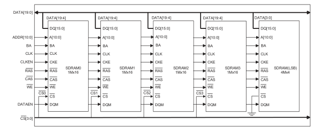
Figure 3-12: Architecture of Memory Array with four 1Mx16 and one 4Mx4 SDRAMs
36 of 60
Page 37
All elements in the array can be simultaneously selected for command execution by activating the chip select signals or commands can be directed to a particular element in the array by activating the chip select signal for that element and deactivating the chip select signal for the others. Figure 3-13: Memory Array Architecture with Four 4MX16 and One 16MX4 SDRAMs shows the pin connections (and slightly different addressing requirements) needed for more common 64M SDRAMs within a memory array. The number of memories for a given format conversion remains the same independent of memory (16M or 64M) being used.
| A[19:0] BA R[10:0] CLK CLKEN RAS CAS WE ATAEN CS[3:0] | |
| DATA[19:4] DATA[19:4] DATA[19:4] DATA[19:4] DATA[3:0] DQ[15:0] DQ[15:0] DQ[15:0] DQ[15:0] DQ[3:0] BA[0] BA[0] BA[0] BA[0] BA[0] A[10:0] A[10:0] A[10:0] A[10:0] A[10:0] CLK CLK CLK CLK CLK CKE CKE CKE CKE CKE RAS RAS RAS RAS RAS SDRAM0 SDRAM1 SDRAM2 SDRAM3 SDRAM(LSB) CAS 4Mx16 CAS 4Mx16 CAS 4Mx16 CAS 4Mx16 CAS 16Mx4 WE WE WE WE WE CS0 CS1 CS2 CS3 CS CS CS CS CS DQM DQM DQM DQM DQM A[11] A[11] A[11] A[11] A[11] BA[1] BA[1] BA[1] BA[1] BA[1] |
DATA[19:0]
ADDR[10:0]
Figure 3-13: Memory Array Architecture with Four 4MX16 and One 16MX4 SDRAMs
To reduce system cost, the memory array architecture is made scalable. That is, when transposing smaller image sizes or when processing 8-bit images, a lesser number of SDRAMs per memory array are required.
Table 3-5: Minimum SDRAM Configurations for Mode 8 (default mode) shows the memory requirements for various format conversions.
37 of 60
Page 38
Table 3-5: Minimum SDRAM Configurations for Mode 8 (default mode)

2048 x 2048
4 (1Mx16) and 1
4 (1Mx16)
0
00
0
00
(4Mx4)
2048 x 1536
3 (1Mx16) and 1
3 (1Mx16)
0
01
0
01
(4Mx4)
2048 x 1024
2 (1Mx16) and 1
2 (1Mx16)
0
10
0
10
(4Mx4)
2048 x 512
1 (1Mx16) and 1
1 (1Mx16)
0
11
0
11
(4Mx4)
a. max(a, b) = a when a >= b, else b when a < b. b.MDL stands for the parameter MODE_16_LEFT. c.MCL stands for the parameter MEM_CONFIG_LEFT. d.MDR stands for the parameter MODE_16_RIGHT. e.MCR stands for the parameter MEM_CONFIG_RIGHT.
Figure 3-14: Architecture of Memory Array with Lesser Number of SDRAMs per Array shows the memory array architecture when the number of memories is
reduced to 2 SDRAMS and one SDRAM (8 bit processing) per memory array.
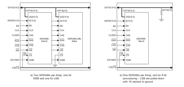
Figure 3-14: Architecture of Memory Array with Lesser Number of SDRAMs per Array
38 of 60
Page 39
3.5.2 SDRAM Specifications
The speed grade of the SDRAM is chosen depending on the processing clock frequency. For example, if the processing clock is running at 74.25MHz, SDRAM with a speed grade of -10 or 100MHz should be selected.
3.5.3 Special Processing
3.5.3.1 Model 16
To further decrease the memory requirements at the expense of processing time an additional mode is available. Table 3-6: Minimum SDRAM Configurations for Mode 16 summarizes the memory requirements for various format conversions in this mode.
Table 3-6: Minimum SDRAM Configurations for Mode 16

1024 x 2048
2 (1Mx16) and 1
2 (1Mx16)
1
10
1
10
(4Mx4)
1024 x 1024
1 (1Mx16) and 1
1 (1Mx16)
1
11
1
11
(4Mx4)
a.max (a, b) = a when a >= b, else b when a < b. b.MDL stands for the parameter MODE_16_LEFT. c.MCL stands for the parameter MEM_CONFIG_LEFT. d.MDR stands for the parameter MODE_16_RIGHT. e.MCR stands for the parameter MEM_CONFIG_RIGHT.
3.5.4 Film Processing
During film processing the GF9320 uses the external signals FILM_FR and OUT_FRST to encode or decode the 3:2 pull-down sequence. The timing of these signals for different modes (film and non-film) is shown in Figure 3-15: 60/60/60 Processing through Figure 3-40: 24p/24p/48p Processing. When the input video is from a film material with 3:2 pull-down, the GF9320 processes the image vertically after combining the even and odd fields to achieve better quality resizing. Duplicate fields in the input sequence are rejected by not writing into the memory. Note that in film modes memory switching does not occur at every field / frame boundary. It depends on the input and output film formats. For example, when the input is video
with 3:2 pull-down, the left array of memories switch only after even and odd fields have been put together. The switching point is shown in the timing diagram by DATAEN_AB and DATAEN_CD signals that are, respectively, the output enable signals for left and right arrays. The GF9320 achieves 3:2 pull-down at the output by separately reading out the even and odd fields.
39 of 60
Page 40
The film sequences shown in Figure 3-15: 60/60/60 Processing through Figure 3- 40: 24p/24p/48p Processing are not the only film frame sequences that the
GF9320 can generate. Note that an X through an input video sequence through Figure 3-16: 30i/24p/24i Processing to Figure 3-34: 48p/24p/24p Processing
denotes a discarded frame when performing 3:2 pulldown compensation. Other input / output film sequences are possible. The input control uses the rising edge
of FILM_FR to set the input film sequence and the film frame reset sent to the output controller. The first TRS V-bit after the rising edge of FILM_FR marks the
beginning of a 3:2 (starting with 3) or 2:2 film sequences.
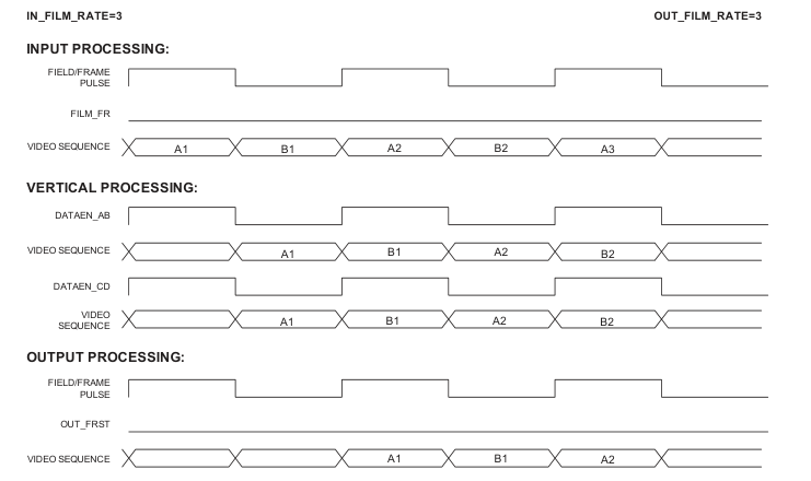
Figure 3-15: 60/60/60 Processing
40 of 60
Page 41
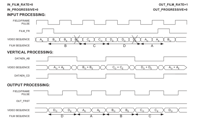
Figure 3-16: 30i/24p/24i Processing
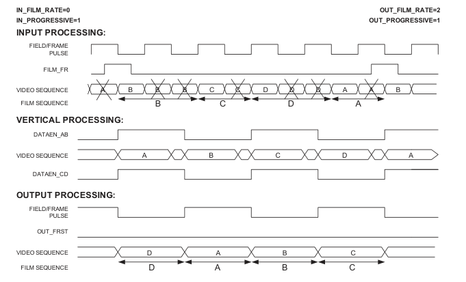
Figure 3-17: 60p/24p/24p Processing
41 of 60
Page 42
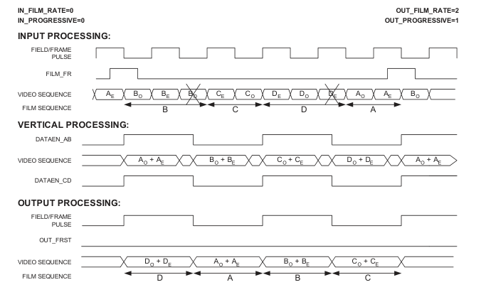
Figure 3-18: 30i/24p/24p Processing
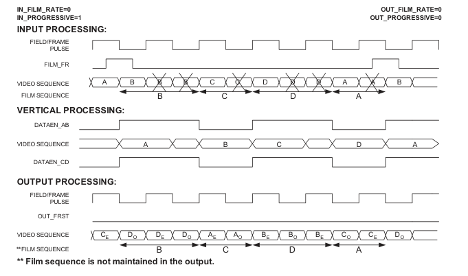
Figure 3-19: 60p/24p/30i Processing
42 of 60
Page 43
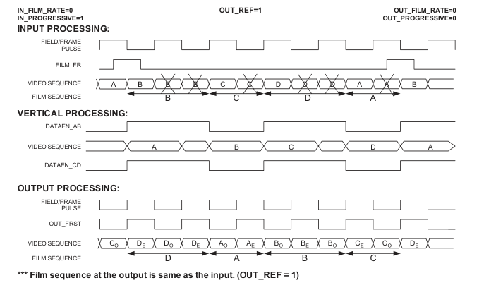
Figure 3-20: 60p/24p/30i (OUT_REF=1) Processing
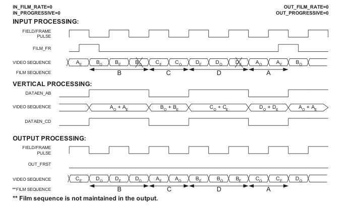
Figure 3-21: 30i/24p/30i Processing
43 of 60
Page 44
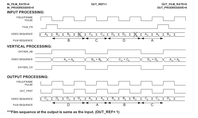
Figure 3-22: 30i/24p/30i (OUT_REF=1) Processing
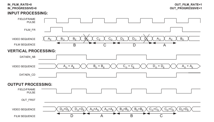
Figure 3-23: 30i/24p/48p Processing
44 of 60
Page 45
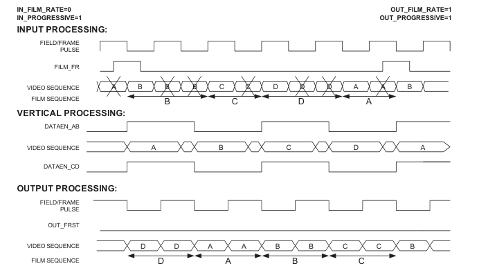
Figure 3-24: 60p/24p/48p Processing
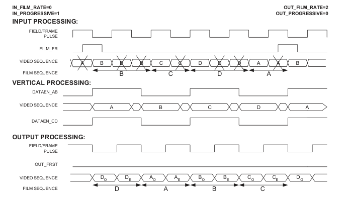
Figure 3-25: 60p/24p/24i Processing
45 of 60
Page 46
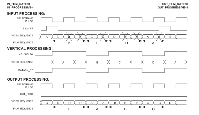
Figure 3-26: 60p/24p/60p Processing
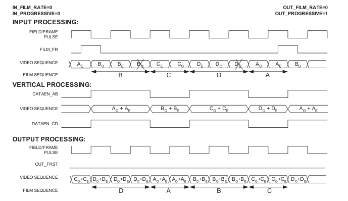
Figure 3-27: 30i/24p/60p Processing
46 of 60
Page 47
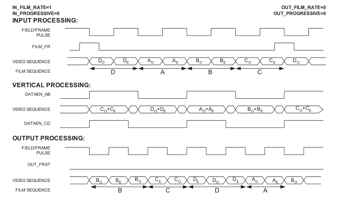
Figure 3-28: 24i/24p/30i Processing
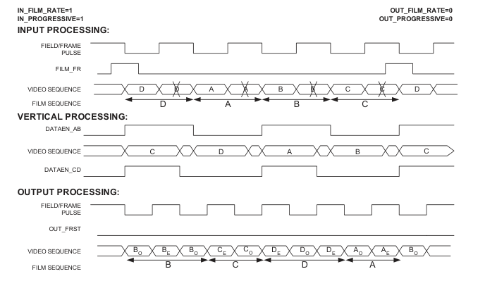
Figure 3-29: 48p/24p/30i Processing
47 of 60
Page 48
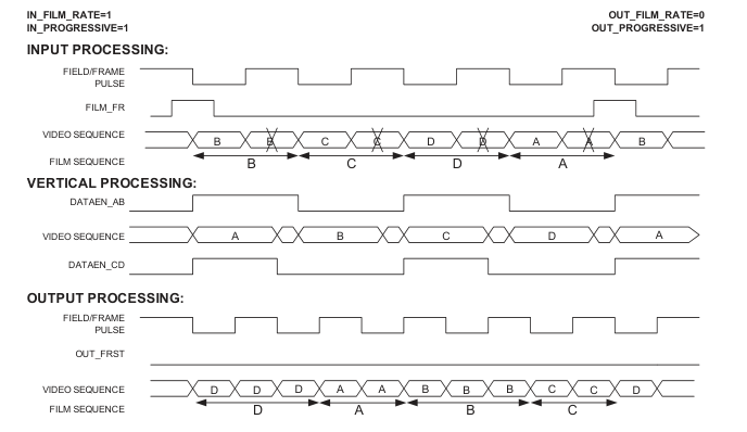
Figure 3-30: 48p/24p/60p Processing
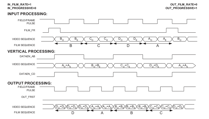
Figure 3-31: 24i/24p/60p Processing
48 of 60
Page 49
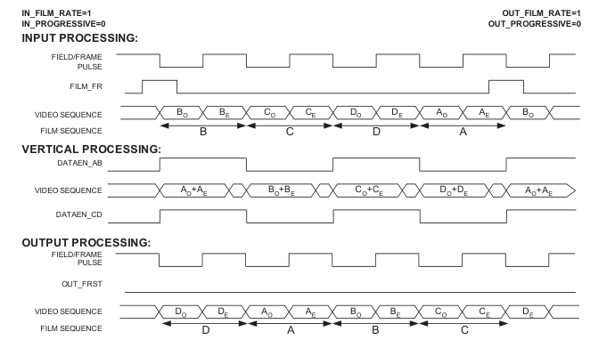
Figure 3-32: 24i/24p/24i Processing
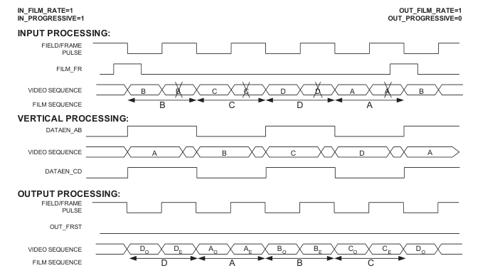
Figure 3-33: 48p/24p/24i Processing
49 of 60
Page 50
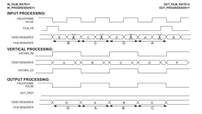
Figure 3-34: 48p/24p/24p Processing
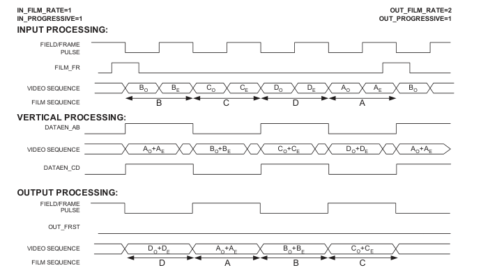
Figure 3-35: 24i/24p/24p Processing
50 of 60
Page 51
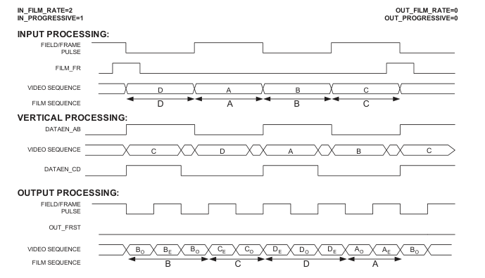
Figure 3-36: 24p/24p/30i Processing
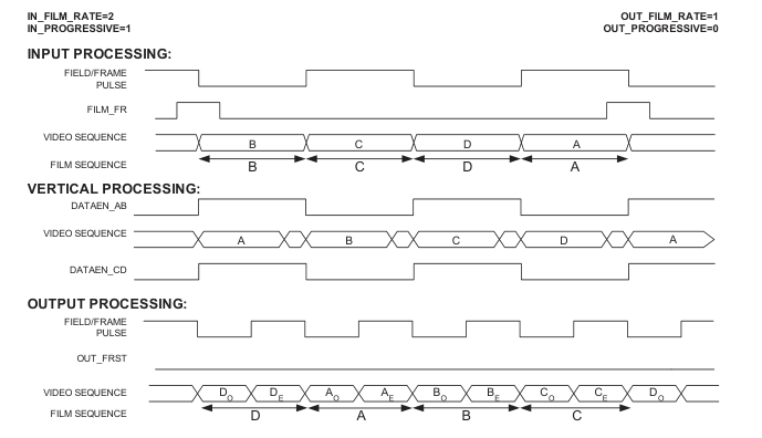
Figure 3-37: 24p/24p/24i Processing
51 of 60
Page 52
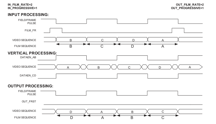
Figure 3-38: 24p/24p/24p Processing
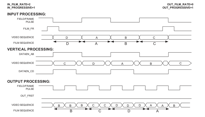
Figure 3-39: 24p/24p/60p Processing
52 of 60
Page 53
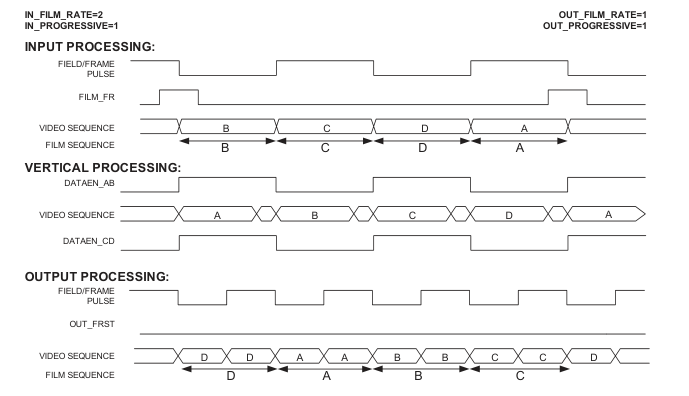
Figure 3-40: 24p/24p/48p Processing
During film processing there is a possibility that for some conversions the GF9320 could violate the refresh period (64 ms) of the SDRAM. If a violation is found
(IN_REFR_LEFT or OUT_REFR_RIGHT = '1'), then the appropriate (left / right) refresh bit should be activated in the download stream of parameters to the
GF9320. Alternatively, Table 3-7: Input and Output Formats Requiring Refresh can be used to determine which input and output formats require refresh bits to be active.
Table 3-7: Input and Output Formats Requiring Refresh
Input Format IN_REFR_LEFT=1
Output Format OUT_REFR_RIGHT=1
24p/25p
24p/25p
48p/50p
30i/60p with 3:2 pull-down
53 of 60
Page 54
3.5.5 Processing Delay
Processing delay for video through the GF9320 depends on the conversion. Table 3-8: Processing Delay for Various Conversions shows the processing delay for different film and non-film modes.
Table 3-8: Processing Delay for Various Conversions
Conversion
Delay (Input Frames / Fields)
[frame / field modes - 60Hz V processing] Note: All other frame rates are identical with appropriate time scaling
30i J 30i
1/30 seconds (2 fields)
30i J 60p
1/30 seconds (2 fields)
60p J 30i
1/30 seconds (2 frames)
60p J 60p
1/30 seconds (2 frames)
[2:2 modes - 30Hz V processing]
30i J 30p
1/15 seconds (4 fields)
60p J30p
1/15 seconds (4 frames)
30p J 30i
1/15 seconds (2 frames)
30p J 60p
1/15 seconds (2 frames)
30i J 30i
1/15 seconds (4 fields)
30i J 60p
1/15 seconds (4 fields)
[3:2 modes - 24Hz V processing]
30i J 30i
1/10-1/12 seconds (5-6 fields)
30i J 60p
1/10-1/12 seconds (5-6 fields)
30i J 24p
3/40-1/12 seconds (4.5-5 fields)
30i J 24i
3/40-1/12 seconds (4.5-5 fields)
60p J 24p
3/40-1/12 seconds (4.5-5 fields)
60p J 24i
3/40-1/12 seconds (4.5-5 fields)
24i J 30i
3/40-1/12 seconds (3.6-4 fields)
24i J 60p
3/40-1/12 seconds (3.6-4 fields)
24p J 30i
3/40-1/12 seconds (1.8-2 frames)
24p J 60p
3/40-1/12 seconds (1.8-2 frames)
54 of 60
Page 55
3.5.6 Pin Descriptions
The GF9320 uses the transpose memory bus interface signals to communicate with external memory (SDRAMs). The GF9320 is the master device on the bus interface and it controls the timing of the address and data flow. Each signal in the bus interface is described as follows:
3.5.6.1 Address Bus
ADDR_A[10:0], ADDR_B[10:0], ADDR_C[10:0], ADDR_D[10:0]
The address bus is shared by all the memories in the array. The address bus bit BA_A (Bank Select) selects which bank is to be active in memory array. BA_A low selects bank A and BA_A high selects bank B within the memory. During a bank activate command cycle, ADDR_A[10:0] defines the row address when sampled at the rising clock edge. During a read / write cycle, ADDR_A[9:0] defines the column address when sampled at the rising clock edge. In addition to the column address ADDR_A10 is used to invoke auto-precharge operation.
Similarly, ADDR_B[10:0], ADDR_C[10:0], ADDR_D[10:0] form the address bus of memory arrays B, C and D respectively.
3.5.6.2 Data Bus
DATA_A[19:0], DATA_B[19:0], DATA_C[19:0], DATA_D[19:0]
The data bus is bi-directional. Valid data is driven on the data bus by the GF9320 during write cycle, which is accepted back by the GF9320 during the read cycles. These cycles involve transfers of bursts of data between the SDRAM core and registers of GF9320. Luminance data Y[9:2] are available on DATA_A/B/C/ D[19:12] while least significant bits Y[1:0] are available on DATA_A/B/C/D[3:2]. Colour difference data C[9:2] are available on DATA_A/B/C/D[11:4] while least significant bits C[1:0] are available on DATA_A/B/C/D[1:0].
3.5.6.3 Command Bus
[RAS_A, CAS_A, WE_A], [RAS_B, CAS_B, WE_B], [RAS_C, CAS_C,
WE_C], [RAS_D, CAS_D, WE_D]
These bus signals are asserted by the GF9320 when commands have to be executed on the SDRAM memory array A. Similarly, [RAS_B, CAS_B, WE_B], [RAS_C, CAS_C, WE_C] and [RAS_D, CAS_D, WE_D] are asserted to execute commands on memory array B, C and D respectively. These signals are considered valid only if the respective CS pin is low during the active edge of the clock.
55 of 60
Page 56
CKEN_A, CKEN_B, CKEN_C, CKEN_D
CKEN_A, CKEN_B, CKEN_C and CKEN_D are used to drive memory arrays A, B, C and D respectively. CKEN input suspends data (i.e. read data remains valid and write data is inhibited) during an active read or write. The GF9320 activates CKEN_A and CKEN_B signals during field / frame write cycle to drop pixels. CKEN_C and CKEN_D are activated during field / frame read cycle to hold pixel values. These signals are considered valid only if the respective CS pin is low during the active edge of the clock.
CS_A[3:0], CS_B[3:0], CS_C[3:0], CS_D[3:0]
The CS_A[3:0] signals from the GF9320 allows selection of individual or multiple SDRAMs within the memory array A. The appropriate SDRAM(s) is selected when the respective CS_A[3:0] pin is active low on the rising edge of clock. CS_B[3:0], CS_C[3:0] and CS_D[3:0] select SDRAMs within memory arrays B, C and D respectively.
DATAEN_AB, DATAEN_CD
These signals are driven by the GF9320 only during start-up to prevent data contention. When sampled high, it places the data bus buffers within the SDRAM in a high impedance state. After successful initialization, DATAEN_AB and DATAEN_CD stay low until the next power-up reset. DATAEN_AB is shared by memories in banks A and B, while DATAEN_CD is shared by memories in banks C and D.
CK_A, CK_B, CK_C, CK_D
CK_A, CK_B, CK_C and CK_D are clock signals, which drive the SDRAMs clock pins in memory array A, B, C and D respectively.
56 of 60
Page 57
3.6 Output Processor
A block diagram of the output processor is shown in Figure 3-41: Output Processor Block Diagram. The output processor consists of three major functions:
1. Colour difference over-sample
2. Matrix conversion
3. Output format
The colour difference over-sample function is necessary for colour matrix conversion and to provide a 4:4:4 output. The colour difference over-sample block
also performs colour background insertion and horizontal edge shaping. Horizontal edge shaping is done to eliminate overshoot on edges when the scaled output
does not fill the entire output raster. That is, when OUT_HSTART is greater that 0 for left edge shaping and when OUT_HSTOP is less than OUT_HLEN_ACT for
right edge shaping. A programmable flat matte colour background is inserted into the output non-live video. Note that the colour background is inserted prior to the
matrix conversion. This means that the downloaded background colour is in the input colour space coordinates.
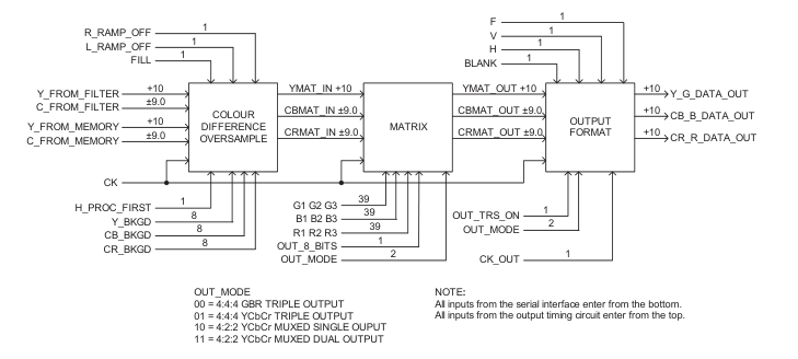
Figure 3-41: Output Processor Block Diagram
The matrix block performs the following operations:
– 64) + ⋅
+ ⋅
G1 ⋅ (
YMATIN
G2 CBMATIN G3 CRMATIN
=
+
---------------------------------------------------------------------------------------------------------------------------------------------
64
YMATOUT
1024
– +
+
B1 ⋅ (
64) ⋅
⋅
YMATIN
B2 CBMATIN B3 CRMATIN
=
+
--------------------------------------------------------------------------------------------------------------------------------------------
PBMATOUT
COFFSET
1024
57 of 60
Page 58
– 64) + ⋅
+ ⋅
R1 ⋅ ( YMATIN
R2 CBMATIN R3 CRMATIN
-------------------------------------------------------------------------------------------------------------------------------------------- =
+ COFFSET
PRMATOUT
1024
where YMATIN, CBMATIN and CRMATIN are the inputs to the matrix; YMATOUT, CBMATOUT and CRMATOUT are the outputs of the matrix; and G1, G2, G3, B1, B2, B3, R1, R2 and R3 are the matrix coefficients;
COFFSET is given by
64 OUT_MODE = 0 = COFFSET 512 otherwise
and 1024 is the gain of the matrix.
The matrix coefficients provide +6dB of range for gain adjustments. The Cb and Cr components at the input to the matrix are in 2's complement format. The B and R components at the output of the matrix are unsigned in GBR output mode (OUT_MODE=0) and are offset binary in YCbCr output mode (OUT_MODE=1, 2 or 3). The matrix coefficients are completely programmable and are downloaded as described in the 3.2 Serial Interface Control.
The output format block formats the data into one, two or three channels according to the OUT_MODE parameter and inserts the output format TRS. If TRS is enabled, the data is clipped to 4 and 1019 for 10-bits or 1 and 254 for 8-bits.
3.7 Output Timing Control
The output timing and control block determines the output video data timing. This block contains horizontal and vertical counters based on the output format parameters. The output timing is adjusted relative to the reference by using the LINE_ADV and H_POS parameters. The output reference is either the input TRS (if OUT_REF = 0) or the OUT_FRST pin on the GF9320 (if OUT_REF = 1). This provides for internal or external lock capability. The LINE_ADV parameter advances the output video data by LINE_ADV output lines. The H_POS parameter delays the output video data by H_POS samples. The range of H_POS is one output line or OUT_HLEN_TOT samples.
Only limited ranges of input / output timing relationships are available by using the GF9320. In general, there are 2 fields / frames of delay through the GF9320. It is not possible for the GF9320 to have an output timing relationship such that the last active output line occurs after the SDRAM field / frame switch point.
58 of 60
Page 59
4. Package Dimensions
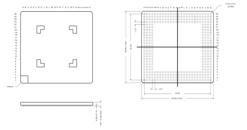
Figure 4-1: Package Dimensions
59 of 60
Page 60
5. Revision History
Changes and / or Modifications
Version ECR
Date
Corrections to address pins: ADDR_A[10:0], ADDR_B[10:0], ADDR_C[10:0], ADDR_D[10:0],
7
134925
BA_A, BA_B, BA_C and BA_D.
Changed BOUT description. Changed template.
6
133502 June 2004
November 2002 Add OUT_VLIVE issue and workaround - Change RST, SIF_RST, CS, RAS, CAS and WE
5
pin descriptions to active low. Make same changes throughout DS. -Make 60I->30i changes for consistency.
4
May 2002
Updating GF9320.
September 2001 Remove all “Preliminary & Confidential” water marks & references with the document.
3
Correction required for both Figure 15 and the table titled “Output Signal Timing
2
July 2001
Specification”.
Correction to figure on page 2 & other improvements.
1
June 2001
Creating Preliminary Data Sheet.
0
June 2001
GENNUM CORPORATION
Mailing Address: P.O. Box 489, Stn. A, Burlington, Ontario, Canada L7R 3Y3 Tel. +1 (905) 632-2996 Fax. +1 (905) 632-5946 Shipping Address: 970 Fraser Drive, Burlington, Ontario, Canada L7L 5P5
GENNUM JAPAN CORPORATION
Shinjuku Green Tower Building 27F, 6-14-1, Nishi Shinjuku, Shinjuku-ku, Tokyo, 160-0023 Japan Tel. +81 (03) 3349-5501, Fax. +81 (03) 3349-5505
GENNUM UK LIMITED
25 Long Garden Walk, Farnham, Surrey, England GU9 7HX
TEL. +44 (0)1252 747 000 FAX +44 (0)1252 726 523
Gennum Corporation assumes no responsibility for the use of any circuits described herein and makes no representations that they are free from patent infringement.
© Copyright June 2001 Gennum Corporation. All rights reserved. Printed in Canada
www.gennum.com
60 of 60