

 Download PDF
GCBC040-1B ALPS
Document overview
- PDF pages: 16
Technical content
Page 1
Current sensor for PW Board mounting
Data sheet
Rev.1.5 e EC 2017.03.28
Attention: Modifications on specification, size, etc., may be carried out for improvement without notice.
Page:1/16
Page 2
Table of contents
- Introduction ................................................................................................................................... 3 2. Features and Advantages ............................................................................................................ 3 3. Principle ......................................................................................................................................... 3 4. Applications ................................................................................................................................... 3 5. Block Diagram and Typical Application...................................................................................... 4
5.1. Block Diagram .......................................................................................................................... 4 5.2. Typical Application ................................................................................................................... 4 6. Dimensions and Terminal Designation ....................................................................................... 7 7. Operating Characteristics ............................................................................................................ 8 7.1. Absolute Maximum Ratings ..................................................................................................... 8
7.2. Operating Condition ................................................................................................................. 8 7.3. Recommended Operating Condition ........................................................................................ 8 7.4. Electrical Characteristics (No Load, Vdd=5.0V, Ta=25°C) ...................................................... 8 7.5. Electrical Characteristics (RL=10kΩ, Vdd=5.0V, Ta=25°C)..................................................... 9 7.6. Start-up timing ........................................................................................................................ 10 7.6.1. Start-up ........................................................................................................................... 10
7.6.2. Low voltage detection ..................................................................................................... 10 7.7. Influence from the ambient magnetic field ............................................................................. 11 8. Characteristic Definitions ........................................................................................................... 12 9. Characteristic Data...................................................................................................................... 14 10. Recommended Soldering Conditions ................................................................................... 15
10.1. Manual Soldering ............................................................................................................... 15 11. Referential Land Pattern ......................................................................................................... 15 12. Extras ........................................................................................................................................ 16
Attention: Modifications on specification, size, etc., may be carried out for improvement without notice.
Page:2/16
Page 3
1. Introduction
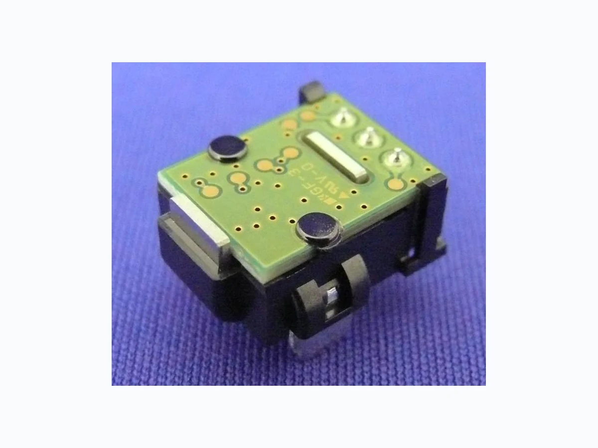
Current sensor GCBC series is for use on the electronic measurement of DC, AC, or pulsed currents with no contact.
2. Features and Advantages
Coreless, small and lightweight(3g) design with high sensitivity magneto-resistive(MR) elements. Low primary-conductor resistance: 60μΩ. Good linearity: ±0.5%F.S. +5V single power supply. Operating temperature: -40°C~+105°C. DC and AC current measurement with quick response.
3. Principle
Current sensor detects the magnetic induction generated by the primary current to be measured. In the module, MR element with conditioning IC is located on the bus bar (path of the primary current). The magnetic field control board is arranged around bus bar and MR element so that module output with high sensitivity can be made. On the other hand, the output error by outer magnetic field, which has no relationship to the magnetic induction of primary current, is decreased.
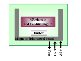
Fig.3-1 Principle of measurement
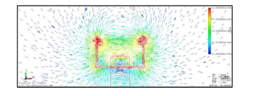
Fig.3-2 The magnetic induction generated by the primary current (simulation)
4. Applications
Motor drivers and general-purpose inverters, PV Inverter systems, Server power supplies, Packaged air-conditioning units, NC machine tools and other industrial and etc...
Attention: Modifications on specification, size, etc., may be carried out for improvement without notice.
Page:3/16
Page 4
5. Block Diagram and Typical Application
5.1. Block Diagram
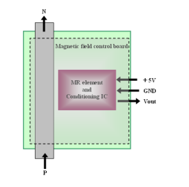
Fig.5-1 Block Diagram of the module
5.2. Typical Application Refer to chapter 7.3 for the recommended operating condition of the load.
(1) Basic connection
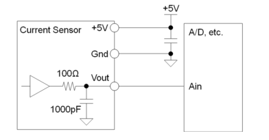
Fig.5-2 Basic connection
\* Current sensor has a LPF with coefficients described in above figure. \* Refer electrical characteristics to chapter 7.4, if RL can be regarded as no-load.
Attention: Modifications on specification, size, etc., may be carried out for improvement without notice.
Page:4/16
Page 5
(2) 3.3V input for A/D
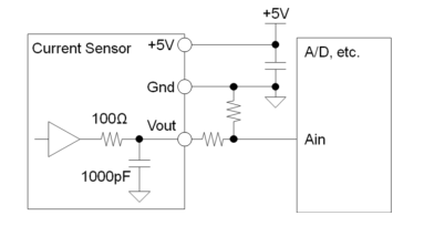
Fig.5-3 3.3V input for A/D
\* Use step down resistance to divide output voltage of the current sensor, if input voltage of A/D is 3.3V.
(3) External filter circuit
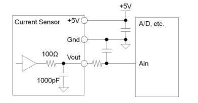
Fig.5-4 External filter circuit
\* Mount a LPF, if necessary. \* Note that Two-stage LPF configuration due to connect an externally LPF, since a current sensor has a built-in LPF.
(4) External filter circuit (in multiple)
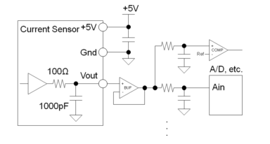
Fig.5-5 External filter circuit(in multiple)
\* Mount an op-amp buffer, if necessary.
Attention: Modifications on specification, size, etc., may be carried out for improvement without notice.
Page:5/16
Page 6
(5) Output treatment for the unknown state Start up time is necessary for this product. During that time, output signal becomes Hi-Z. If you want to fix the output voltage during that timing, please see below as your reference.
Pull-up
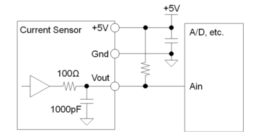
Fig.5-6 Pull-up
\* Fix the potential to 5V in the period of the Hi-Z, if it is necessary to keep +5V during start-up or low voltage detection as an output signal. \* Refer to chapter 7.6 regarding start-up timing. \* Note that output load RL of the current sensor is not less than 10kΩ. Voltage Vout of the output is the resistance divider ratio of the 100Ω of built-in filter, if connect a pull-up resistor. Therefore, the use of precision resistors, such as 1% so that the error variation of the resistance partial pressure is not increased.
Pull-down
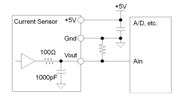
Fig.5-7 Pull-down
\* Fix the potential to 0V in the period of the Hi-Z, if it is necessary to keep 0V during start-up or low voltage detection as an output signal. \* Refer to chapter 7.6 regarding start-up timing. \* Note that output load RL of the current sensor is not less than 10kΩ. Voltage Vout of the output is the resistance divider ratio of the 100Ω of built-in filter, if connect a pull-up resistor. Therefore, the use of precision resistors, such as 1% so that the error variation of the resistance partial pressure is not increased. \* Refer electrical characteristics to chapter 7.5, if RL can be regarded as 10kΩ.
Attention: Modifications on specification, size, etc., may be carried out for improvement without notice.
Page:6/16
Page 7
6. Dimensions and Terminal Designation
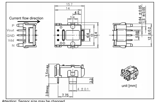
Fig.6-1 Dimensions
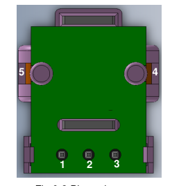
Table6-1 Terminal list table
| No. | Name | Description |
|---|---|---|
| 1 | Vout | Signal Output |
| 2 | GND | Ground |
| 3 | VDD | +5V Power Supply |
| 4 | N | Primary Current terminal (-) |
| 5 | P | Primary Current terminal (+) |
Fig.6-2 Pin assignment
Attention: Modifications on specification, size, etc., may be carried out for improvement without notice.
Page:7/16
Page 8
7. Operating Characteristics
7.1. Absolute Maximum Ratings
| No | Parameter | Symbol | Min | Typ | Max | Unit | Note |
|---|---|---|---|---|---|---|---|
| 1 | Supply Voltage | Vdd | -0.3 | 5.5 | V | Vdd pin | |
| 2 | Output Current (VOUTpin) | Iout | -1.1 | 1.1 | mA | Vout pin, continuously | |
| Iout | -40 | 40 | mA | Vout pin, pulse width 1μs, Period 1kHz | |||
| 3 | Storage temperature | Ts | -40 | 105 | °C | ||
| 4 | Storage ambient magnetic field | Bs | -8 | 8 | mT | ||
| 5 | Maximum current (over current) | Ipoc | -110 | 110 | A | ||
| 6 | Maximum continuous current | Irmcnt | -40 | 40 | A |
7.2. Operating Condition
| No | Parameter | Symbol | Min | Typ | Max | Unit | Note |
|---|---|---|---|---|---|---|---|
| 1 | Supply Voltage | Vdd | 4.85 | 5.00 | 5.15 | V | ±3%(5.0V±0.15V) |
| 2 | Primary Current Measuring Range | Ir | -40 | 40 | A | DC±40A | |
| 3 | Operating Temperature | Ta | -40 | 105 | °C |
7.3. Recommended Operating Condition
| No | Parameter | Symbol | Min | Typ | Max | Unit | Note |
|---|---|---|---|---|---|---|---|
| 1 | Output Current | Iout | -0.5 | 0.5 | mA | VOUT pin | |
| 2 | Load capacity | CL | 100 | pF | VOUT pin |
7.4. Electrical Characteristics (No Load, Vdd=5.0V, Ta=25°C)
| No | Parameter | Symbol | Min | Typ | Max | Unit | Note |
|---|---|---|---|---|---|---|---|
| 1 | Offset Voltage (*1) | Vof | 2.500 | V | Vdd×1/2 | ||
| 2 | Offset Thermal Drift | TcVof | ±0.8 | mV/°C | -40~+105°C | ||
| 3 | Sensitivity (*2) | Vo | 50.0 | mV/A | |||
| 4 | Sensitivity Temperature Drift | TcVo | ±0.02 | %/°C | -40~+105°C | ||
| 5 | Linearity | e L | ±0.2 | %FS | FS=Full Scale | ||
| 6 | Response Time | tr | 1 | μs | Input Current : di/dt=40A/μs, 80%Response | ||
| 7 | Current Consumption | Iddmax | 13 | mA | |||
| 8 | Isolation Voltage | Vins | 750 | V | AC 50/60Hz,60s Sensor Unit | ||
| 9 | Insulation Resistance | Rins | 500 | MΩ | DC500V Signal Terminal Batch With Bus bar | ||
| 10 | Hysteresis Error of Vof (*3) | Voh | ±10 | mV | Primary Current Measuring Range | ||
| 11 | Primary Conductor Resistance (*3) | R 1 | 60 | μΩ |
Attention: Modifications on specification, size, etc., may be carried out for improvement without notice.
Page:8/16
Page 9
7.5. Electrical Characteristics (RL=10kΩ, Vdd=5.0V, Ta=25°C)
| No | Parameter | Symbol | Min | Typ | Max | Unit | Note |
|---|---|---|---|---|---|---|---|
| 1 | Offset Voltage (*1, *3) | Vof | 2.475 | V | Vdd=+5.00V | ||
| 3 | Sensitivity (*2, *3) | Vo | 49.5 | mV/A |
Note: Only characteristics No.1 and 3 are different from No-load.
\* 1 Offset voltage will change in ratiometric to supply voltage. \* 2 Sensitivity does not change in the ratiometric to the supply voltage. \* 3 Reference only.
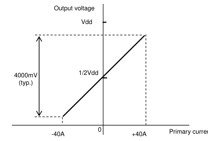
Fig.7-1 Current vs. output voltage
Attention: Modifications on specification, size, etc., may be carried out for improvement without notice.
Page:9/16
Page 10
7.6. Start-up timing 7.6.1. Start-up This current sensor has a conditioning IC. Conditioning IC will start the start up sequence under operation voltage after power supply is turned on. The transition to the normal state through the start-up time, Vout output will output a valid voltage.
7.6.2. Low voltage detection If the supply voltage drops to the operation voltage by instantaneous power failure, output signal will be stopped and become a Hi-Z by low voltage detention. To returns from the instantaneous power failure state, conditioning IC will restart the operation with operation voltage. Transition to the normal state through the start-up time, Vout output will output a valid voltage. During transition time to the normal operation, Vout signal has some variation (flapping) as an output signal, since closed loop of magnetic equilibrium expression is controlled by feedback to be equilibrium.
Start up timing
| No | Parameter | Symbol | Min | Typ | Max | Unit | Note |
|---|---|---|---|---|---|---|---|
| 1 | Operation start voltage | Vopu | 4.05 | 4.4 | 4.75 | V | |
| 2 | Operation stop voltage | Vopl | 3 | 3.5 | 4.5 | V | |
| 3 | Start-up time | Tstup | 1 | 30 | ms |
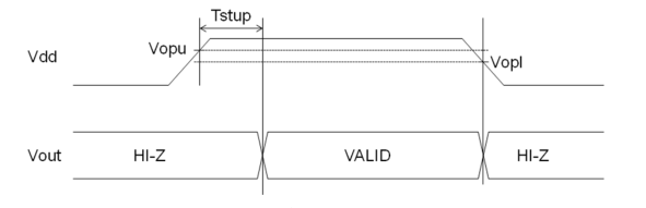
Fig.7-2 Start up timing
Attention: Modifications on specification, size, etc., may be carried out for improvement without notice.
Page:10/16
Page 11
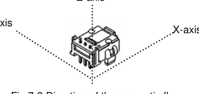
7.7. Influence from the ambient magnetic field This current sensor uses a magnetic sensor for a current detecting. It is influenced by ambient magnetic field. Reference information to minimize the influence from the ambient magnetic are described below.
The transformer and the inductor generate the leakage flux , It is affected by the accuracy of the current sensor by the leakage flux. It especially most affected to the magnetic flux of the X-axis direction. Please decide component location after your evaluation.
If the current path running parallel in close to the current sensor, The accuracy of the current sensor is affected by magnetic flux from the another current path. It especially most affected to the magnetic flux of the Y-axis direction. Please decide PCB pattern design after your evaluation.
Z-axis
Y-axis
Fig.7-3 Direction of the magnetic flux
Attention: Modifications on specification, size, etc., may be carried out for improvement without notice.
Page:11/16
Page 12
8. Characteristic Definitions
The contents of the main characteristics are shown below. Standard conditions and the standard state in each item are defined below.
Standard condition: Ambient temperature 25°C The state of the standard: Supply voltage (DC+5.00V) with No Load.
(1) Offset Voltage The output voltage when the primary current is 0A.
(2) Offset Thermal Drift Change of the offset voltage within the range of the operating temperature. The value is the amount of the change per 1 degree calculated with the output at 25 degrees as the reference.
(3) Sensitivity The slope of the estimated output. The least squares method from the output voltages for the primary current within rating is used.
(4) Sensitivity Temperature Drift Change of the gain within the operating temperature range. The value is the ratio of the change per 1 degree calculated with the gain at 25 degrees as the reference.
(5) Linearity The error of the output voltage between measured and estimated. The least squares method from the output voltages at rated primary current, its half current, 0A(offset voltage), is used. The value is calculated using equation;
Non Linearity = { (Measured Vout - Estimated Vout) / (Output voltage at positive maximum current of measurement current range - Output voltage at negative maximum current of measurement current range) } × 100(%FS)
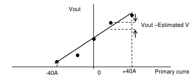
Fig.8-1 Non linearity
Attention: Modifications on specification, size, etc., may be carried out for improvement without notice.
Page:12/16
Page 13
(6) Response Time Fig.8-2 shows the response time of output (dT) when primary current is square wave which have 40A/us rise/fall time. Response time is defined as the time between 80% change point of input wave and output.
| 80% | |
| 80% |
dT
Fig.8-2 Response Time
(7) Current Consumption The bus bar rating pass an electric current this current consumption measure.
(8) Isolation Voltage 750V in the AC voltage, 50Hz, and 60sec are impressed to the bus bar with the control terminal batch under.
(9) Insulation Resistance It measures between the control terminal batch and the bus bar with Meg ohm meter (DC500V) under the standard condition.
(10) Hysteresis Absolute value of the difference of the output when the primary current is 0A between after rated positive primary current is added and negative one is added.
Attention: Modifications on specification, size, etc., may be carried out for improvement without notice.
Page:13/16
Page 14
9. Characteristic Data
Example of typical characteristics.
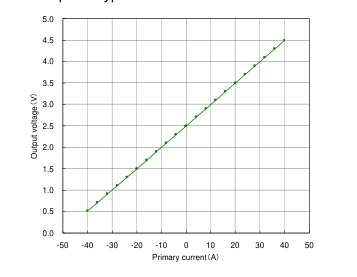
Fig.9-1 Output voltage
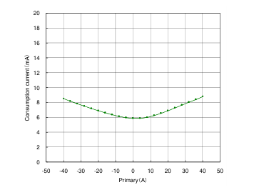
Fig.9-3 Consumption Current
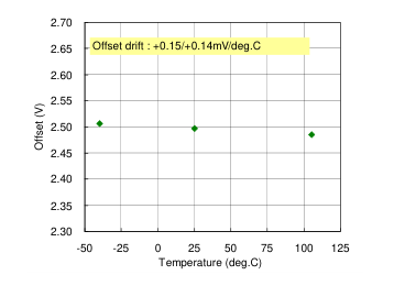
Fig.9-5 Offset voltage vs. temperature
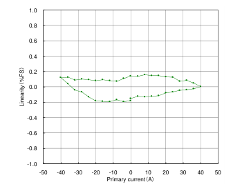
Fig.9-2 Linearity
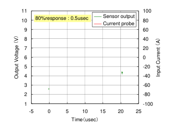
Fig.9-4 Response time
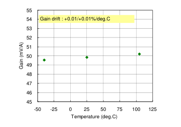
Fig.9-6 Gain vs. temperature
Attention: Modifications on specification, size, etc., may be carried out for improvement without notice.
Page:14/16
Page 15
10. Recommended Soldering Conditions
10.1. Manual Soldering
| Temperature | 350±5°C |
| Time | 3 sec. max. |
| Number of Times | 2 times max. |
Note: The rise in heat of current sensor is influenced by the solder trowel and the mounting substrate. Please control so that the temperature of the primary current terminal does not exceed 260°C, when the above-mentioned conditions are impossible.
11. Referential Land Pattern
Referential land pattern is shown here.
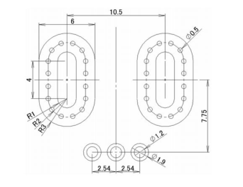
Fig.11-1 Referential Land Pattern
Unit: mm
Attention: Modifications on specification, size, etc., may be carried out for improvement without notice.
Page:15/16
Page 16
12. Extras
All information described in this document is intended only as guidance to explain operation and how to use this product, and we do not warrant that this information is not infringe any intellectual property rights of us and any third party and other rights. In case of using all information described in this document, you agree that you are solely judgment and responsible for it. Therefore, you must be in any way responsible or liable for any damages, expenses or losses incurred by you or third parties arising from the use of this information. Absolute maximum rating is the value that should not be exceeded. When used beyond the conditions in one item, breakage or shift of the characteristics without lead to damage, may affect the
reliability and life. In addition, normal operation is not guaranteed. Electrical characteristics may not be guaranteed, if use more than the operating conditions or the recommended operating conditions. The characteristics on this datasheet are the example with NO load and 10kOhm pull-down. Please note that output voltage varies depending on the load resistance. The primary current must be below rating. The residual output may cause when the current over rating is added. Do not expose the product to strong magnetic field. The residual output may cause. Do not use the product if it is fallen. The residual output may cause. Damage may occur by unusual heat when large or constant primary current is added. The amount of
heat depends on the current and heat radiation. The control wire should be set as short as possible to avoid the outside noise. Before determine placement and wiring of any parts, please be fully evaluated. Magnetic flux leaking from the adjacent magnetic parts and magnetic flux generated from the pattern of the PWB which a large current flows, adversely affect the electrical characteristics. For the export of products which are controlled items subject to foreign and domestic export laws and regulations, you must obtain approval and/or follow the formalities of such laws and regulations. Products must not be used for military and/or antisocial purposes such as terrorism, and shall not be
supplied to any party intending to use the products for such purposes. Unless provided for otherwise, the products have been designed and manufactured for application in equipment and devices which are sold to end users in the market, including audio-visual (AV) equipment, electrical home appliances, office machines, information and communication equipment, and amusement equipment. The products are not intended for use in, and must not be used for, any application for nuclear equipment, driving equipment for aerospace or any other unauthorized use. With the exception of the abovementioned prohibited applications, please contact an Alps sales representative and/or evaluate the total system regarding applicability for applications involving high
levels of safety and liability such as medical equipment, burglar alarm equipment, disaster prevention equipment and undersea equipment. Please also incorporate fail-safe design, protection and redundant circuitry, malfunction protection, and/or fire protection into the complete system to ensure safety and reliability of the total system. Before using products which were not specifically designed for use in automotive applications, please contact an Alps sales representative.
Attention: Modifications on specification, size, etc., may be carried out for improvement without notice.
Page:16/16