


 Download PDF
G1AFS RFE
Document overview
- PDF pages: 3
Technical content
Page 1
■ FEATURES
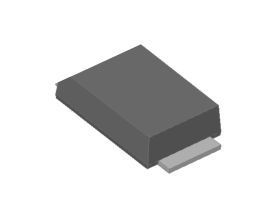
- Low profile package
- Ideal for automated placement
- Glass passivated chip junction
- High forward surge capability
- Meets MSL level 1, per J-STD-020, LF maximum peak of 260 °C
■ TYPICAL APPLICATIONS
For use in general purpose rectification of power supplies, inverters, converters, and freewheeling diodes for consumer and telecommunication.
■ MECHANICAL DATA
- Package: SMAF Molding compound meets UL 94 V-0 flammability rating, RoHS-compliant, halogen-free
- Terminals: Tin plated leads, solderable per J-STD-002 and JESD22-B102
- Polarity: Cathode line denotes the cathode end
■ MAXIMUM RATINGS
Unless otherwise specified)
(Ta=25 °C
| PARAMETER | SYMBOL | UNIT | G1AFS | G1BFS | G1DFS | G1GFS | G1JFS | G1KFS | G1MFS |
|---|---|---|---|---|---|---|---|---|---|
| Device marking code | G1AFS | G1BFS | G1DFS | G1GFS | G1JFS | G1KFS | G1MFS | ||
| Repetitive peak reverse voltage | VRRM | V | 50 | 100 | 200 | 400 | 600 | 800 | 1000 |
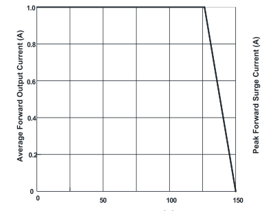
| Average rectified output current @60Hz sine wave, resistance load, TL (Fig.1) | IO | A | 1.0 | ||||||
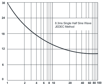
| Surge(non-repetitive)forward current @60Hz Half-sine wave,1 cycle, Ta=25°C | IFSM | A | 30 | ||||||
| Storage temperature | Tstg | °C | -55~+150 | ||||||
| Junction temperature | Tj | °C | -55~+150 | ||||||
■ ELECTRICAL CHARACTERISTICS
(Ta=25°C Unless otherwise specified)
| PARAMETER | SYMBOL | UNIT | TEST CONDITIONS | G1AFS | G1BFS | G1DFS | G1GFS | G1JFS | G1KFS | G1MFS |
|---|---|---|---|---|---|---|---|---|---|---|
| Maximum instantaneous forward voltage drop per diode | VF | V | IFM=1.0A | 1.1 | ||||||
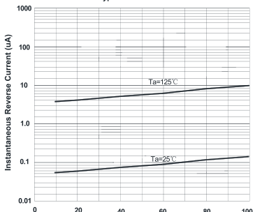
| Maximum DC reverse current at rated DC blocking voltage per diode @VRM=VRRM | IRRM | μA | Ta =25°C | 5.0 | ||||||
| Ta =125°C | 100 | |||||||||
■
THERMAL CHARACTERISTICS (Ta=25
°C Unless otherwise specified)
| PARAMETER | SYMBOL | UNIT | G1AFS | G1BFS | G1DFS | G1GFS | G1JFS | G1KFS | G1MFS |
|---|---|---|---|---|---|---|---|---|---|
| Thermal resistance | RθJ-A | °C/W | 651) | ||||||
| RθJ-L | 251) | ||||||||
Note: (1) Thermal resistance from junction to ambient and from junction to lead mounted on P.C.B. with 0.2" x 0.2" (5.0 mm x 5.0 mm) copper pad areas
Page 1 of 3
Page 2
■CHARACTERISTICS (TYPICAL)
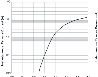
■ PACKAGING INFORMATION
| PREFERED P/N | PACKING CODE | UNIT WEIGHT(g) | MINIMUM IN PACKAGE(pcs) QUA | NER BOX OUTER CARTON NTITY(pcs) QUANTITY(pcs) | DELIVERY MODE |
|---|---|---|---|---|---|
| G1AFS-G1MFS | XO7 | Approximate 0.034 | 3000 | 12000 96000 | 7” reel |
| G1AFS-G1MFS | Omit for S tandard | Approximate 0.034 | 10000 | 20000 160000 | 13” reel |
Page 2 of 3
Page 3
■ OUTLINE DIMENSIONS
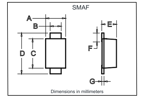
| SMAF | ||
| Dim A | Min 2.40 | Max 2.80 |
| B | 1.35 | 1.45 |
| C | 3.40 | 3.60 |
| D | 4.40 | 4.80 |
| E | 1.05 | 1.25 |
| F | 0.50 | 1.00 |
| G | 0.15 | 0.22 |
■ SUGGESTED PAD LAYOUT
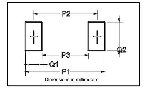
| SMAF | |
| Dim | Millimeters |
| P1 | 6.50 |
| P2 | 4.00 |
| P3 | 1.50 |
| Q1 | 2.50 |
| Q2 | 1.70 |
Page 3 of 3