
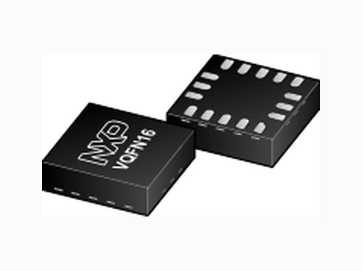
FXLS8471Q, 3-Axis, Linear Accelerometer - Data sheet
Document overview
- Manufacturer or author: NXP Semiconductors
- PDF pages: 86
Technical content
Datasheet sections
- 1 General description
- 2 Features and benefits
- 3 Typical applications
- 4 Ordering information
- 5 Block Diagram
- 6 Pinning information
- 6.1 Pinning
- 6.2 Pin description
- 7 Orientation
- 8 Electrical connections
- 9 Terminology
- 9.1 Sensitivity
- 9.2 Zero-g offset
- 9.3 Self-test
- 10 Digital interfaces
- 10.1 I2C interface characteristics
- 10.1.1 General I2C operation
- 10.1.2 I2C read/write operations
- 10.2 SPI interface characteristics
- 10.2.1 General SPI operation
- 10.2.2 SPI READ/WRITE operations
- 10.2.3 I2C/SPI auto detection
- 10.2.4 Power supply sequencing and I2C/SPI mode
- 11 Absolute maximum ratings
- 12 Mechanical characteristics
- 13 Electrical characteristics
- 14 Temperature sensor characteristics
- 15 Modes of operation
- 16 Embedded functionality
- 16.1 Factory calibration
- 16.3 Low-power modes versus high-resolution
- 16.4 Auto-Wake and Auto-Sleep modes
- 16.5 Free-fall and Motion event detection
- 16.5.1 Free fall detection
- 16.5.2 Motion detection
- 16.6 Transient detection
- 16.7 Pulse detection
- 16.8 Orientation detection
- 16.9 Acceleration vector-magnitude detection
- 17 Register Map
- 18 Register descriptions by functional block
- 18.1 Device configuration registers
- 18.1.1 STATUS register (address 00h)
- 18.1.2 DR_STATUS register (address 00h)
- 18.1.3 F_STATUS register (address 00h)
- 18.1.4 TRIG_CFG register (address 0Ah)
- 18.1.5 SYSMOD register (address 0Bh)
- 18.1.6 INT_SOURCE register (address 0Ch)
- 18.1.7 WHO_AM_I register (address 0Dh)
- 18.1.8 CTRL_REG1 register (address 2Ah)
- 18.1.9 CTRL_REG2 register (address 2Bh)
- 18.1.10 CTRL_REG3 - interrupt control register
- 18.1.11 CTRL_REG4 - interrupt enable register
- 18.1.12 CTRL_REG5 - interrupt routing configuration
- 18.1.13 CTRL_REG6 - register (address 5Bh)
- 18.1.14 CTRL_REG7 - register (address 5Ch)
- 18.2 Auto-Sleep trigger register
- 18.2.1 ASLP_COUNT register (address 29h)
- 18.3 Temperature register
- 18.3.1 TEMP_OUT register (address 51h)
- 18.4 Output data registers
- 18.4.1 OUT_X_MSB, OUT_X_LSB, OUT_Y_MSB,
- 18.5 FIFO registers
- 18.5.1 F_SETUP register (address 09h)
- 18.6 Sensor data configuration registers
- 18.6.1 XYZ_DATA_CFG register (address 0Eh)
- 18.7 High-pass filter register
- 18.7.1 HP_FILTER_CUTOFF register (address
- 18.8 Portrait/Landscape detection registers
- 18.8.1 PL_STATUS register (address 10h)
- 18.8.2 PL_CFG register (address 11h)
- 18.8.3 PL_COUNT register (address 12h) register
- 18.8.4 PL_BF_ZCOMP register (address 13h)
- 18.8.5 PL_THS_REG register (address 14h)
- 18.9 Free-fall and Motion event detection
- 18.9.1 A_FFMT_CFG register (address 15h)
- 18.9.2 A_FFMT_SRC register (address 16h)
- 18.9.3 A_FFMT_THSxxxxxx registers (addresses
- 18.9.4 A_FFMT_COUNT register (address 18h)
- 18.10 Accelerometer vector-magnitude function
- 18.10.1 A_VECM_CFG register (address 5Fh)
- 18.10.2 A_VECM_THS_MSB register (address 60h)
- 18.10.3 A_VECM_THS_LSB register (address 61h)
- 18.10.4 A_VECM_CNT register (address 62h)
- 18.10.5 A_VECM_INITX_MSB register (address
- 18.10.6 A_VECM_INITX_LSB register (address
- 18.10.7 A_VECM_INITY_MSB register (address
- 18.10.8 A_VECM_INITY_LSB register (address
- 18.10.9 A_VECM_INITZ_MSB register (address
- 18.10.10 A_VECM_INITZ_LSB register (address 68h)
- 18.11 Transient (AC) acceleration detection
- 18.11.1 TRANSIENT_CFG register (address 1Dh)
- 18.11.2 TRANSIENT_SRC register (address 1Eh)
- 18.11.3 TRANSIENT_THS register (address 1Fh)
3-Axis, Linear Accelerometer Rev. 3.0 — 13 June 2019 Product data sheet
1 General description
FXLS8471Q is a small, low-power, 3-axis, linear accelerometer in a 3 mm x 3 mm x 1 mm QFN package. FXLS8471Q has dynamically selectable acceleration full-scale ranges of ±2 g/±4 g/±8 g and 14 bits of resolution. Output data rates (ODR) are programmable from 1.563 Hz to 800 Hz. I2C and SPI serial digital interfaces are provided along with several user programmable event detection functions that can be used to reduce the overall system power consumption by off-loading the host processor. FXLS8471Q is guaranteed to operate over the extended temperature range of –40 °C to +105 °C.
2 Features and benefits
- 1.95 V to 3.6 V VDD supply voltage, 1.62 V to 3.6 V VDDIO voltage
- ±2 g/±4 g/±8 g dynamically selectable acceleration full-scale ranges
- Output Data Rates (ODR) from 1.563 Hz to 800 Hz
- Low noise: typically 99 μg/Hz in low-noise mode @ 200-Hz bandwidth
- 14-bit ADC resolution: 0.244 mg/LSB in ±2 g full-scale range
- Embedded programmable acceleration event functions – Freefall and motion detection – Transient detection – Vector-Magnitude change detection – Pulse and tap detection (single and double) – Orientation detection (portrait/landscape)
- Programmable automatic ODR change using Auto-Wake and return to Sleep functions to save power
- 192-byte FIFO buffer, capable of storing up to 32 samples of X/Y/Z data
- Supports SPI interface at up to 1 MHz; I2C Normal (100 kHz) and Fast modes (400 kHz)
- Integrated self-test function
- Integrated temperature sensor with 8-bit output resolution
3 Typical applications
Automotive convenience and security
- Tilt sensing, orientation detection, vibration sensing
- Navigation applications Industrial IOT
- Asset tracking
- Equipment monitoring: vibration analysis, machine health
- Patient and activity monitors Consumer devices
- Wearables
- Portable electronics
4 Ordering information
Table 1. Ordering information
5 Block Diagram
Figure 1. Block diagram
6 Pinning information
6.1 Pinning
16 RST
14 VDD
Figure 2. Pinning
6.2 Pin description
Table 2. Pin Description [2] See Table 4 for I2C address options selectable using the SA0 and SA1 pins.
7 Orientation
Figure 3. Product orientation and axis orientation
8 Electrical connections
ceramic capacitor placed as close as possible to pin 1 of the device. through their internal ESD protection diodes. therefore require a pullup resistor as shown in the application diagram in Figure 4. configured for open drain, external pullup resistors are required.
Figure 4. Electrical connection
9 Terminology
9.1 Sensitivity
0.488 mg/LSB in 4 g mode, and 0.976 mg/LSB in 8 g mode.
9.2 Zero-g offset
the sensor onto a printed circuit board, or after exposure to extensive mechanical stress.
9.3 Self-test
sensor and by the electrostatic self-test force.
10 Digital interfaces
10.1 I2C interface characteristics
Table 3. I2C slave timing values[1] [2] This device does not stretch the low period (tLOW) of the SCL signal. [3] tVD;DAT = time for data signal from SCL low to SDA output. [5] Cb = total capacitance of one bus line in pF. Figure 5. I2C slave timing diagram
10.1.1 General I2C operation
is compliant with fast mode (400 kHz), and normal mode (100 kHz) I2C standards. capacitance). See Table 4 for more information. recognize clock stretching. This device does not employ clock stretching. Table 4. I2C slave address
10.1.2 I2C read/write operations
NXP Semiconductors FXLS8471Q 3-Axis, Linear Accelerometer Product data sheet Rev. 3.0 — 13 June 2019 transmits the data from the requested register. The master does not acknowledge (NAK) the transmitted data, but transmits a stop condition to end the data transfer. Multiple-byte read When performing a multi-byte or burst read, the FXLS8471Q automatically increments the register address read pointer after a read command is received. Therefore, after following the steps of a single-byte read, multiple bytes of data can be read from sequential registers after each FXLS8471Q acknowledgment (AK) is received until a no acknowledge (NAK) occurs from the master followed by a stop condition (SP) signaling an end of transmission. Single-byte write To start a write command, the master transmits a start condition (ST) to the FXLS8471Q, followed by the slave address with the R/W bit set to "0" for a write, and the FXLS8471Q sends an acknowledgment. Then the master (or MCU) transmits the address of the register to write to, and the FXLS8471Q sends an acknowledgment. Then the master (or MCU) transmits the 8-bit data to write to the designated register and the FXLS8471Q sends an acknowledgment that it has received the data. Because this transmission is complete, the master transmits a stop condition (SP) to end the data transfer. The data sent to the FXLS8471Q is now stored in the appropriate register. Multiple-byte write The FXLS8471Q automatically increments the register address write pointer after a write command is received. Therefore, after following the steps of a single-byte write, multiple bytes of data can be written to sequential registers after each FXLS8471Q acknowledgment (ACK) is received.
Figure 6. I2C timing diagram
10.2 SPI interface characteristics
considered as the slave and thus is never initiating the communication. Table 5 and Figure 7 describe the timing requirements for correct operation. Table 5. SPI timing
Figure 7. SPI timing diagram
10.2.1 General SPI operation
the master toggles the SPI clock (SCLK) and transmits data on the MOSI pin. Byte 2: DATA[7],DATA[6],DATA[5],DATA[4],DATA[3],DATA[2],DATA[1],DATA[0].
- Polarity: rising/falling
- Phase: sample/setup
- Order: MSB first Data is sampled during the rising edge of SCLK and set up during the falling edge of SCLK.
10.2.2 SPI READ/WRITE operations
are ignored by the part. The read data is deserialized from the MISO pin. registers, starting from the indicated register address in ADDR[7:0]. by deasserting the CS_B pin (low-to-high transition).
transmitted by the master using the MOSI pin. That is, a transaction is always initiated by master. Figure 8. SPI single-burst read/write transaction diagram devices while the FXLS8471Q is powered down. Table 6. Serial interface pin descriptions
10.2.3 I2C/SPI auto detection
Table 7. I2C/SPI auto detection
10.2.4 Power supply sequencing and I2C/SPI mode auto-detection
extended periods may affect device reliability. Table 8. Maximum ratings Table 9. ESD and latchup protection characteristics permanent damage to the part or cause the part to otherwise fail. can cause permanent damage to the part.
12 Mechanical characteristics
Table 10. Mechanical characteristics VDD = 1.8 to 3.3 V, VDDIO = 1.8 V, T = 25 °C, unless otherwise noted. Typical values represent mean or mean ±1 σ values, depending on the specific parameter. [1] Dynamic range is limited to ±4 g when in the low-noise mode. [3] Post-board mount offset specifications are based on a 2-layer PCB design. [4] Determined through bench evaluation (small number of typical devices measured at room temperature). [5] After post-board mount corrections for sensitivity, cross axis and offset. Refer to AN4399 for more information. [6] Self-test is only exercised along one direction for each sensitive axis. [7] Measured using earth's gravitational field (1 g) with the device oriented horizontally (+Z axis up) and stationary.
Table 11. Electrical characteristics VDD = 1.8 to 3.3 V, VDDIO = 1.8 V, T = 25 °C, unless otherwise noted. Typical values represent mean or mean ±1 σ values, depending on the specific parameter. [1] Time from VDDIO on and VDD > VDD min until I2C/SPI interface ready for operation. [2] Time to obtain valid data from power-down mode to Active mode. [3] Time to obtain valid data from Standby mode to Active mode.
14 Temperature sensor characteristics
Table 12. Temperature characteristics VDD = 1.8 to 3.3 V, VDDIO = 1.8 V, unless otherwise noted. Typical values represent mean or mean ±1 σ values, depending on the specific parameter.
15 Modes of operation
Figure 9. FXLS8471Q power mode transition diagram Table 13. Mode of operation description blocks are shutdown. I2C bus inhibited. disabled. Internal clocks disabled. All blocks are enabled (digital and analog). them, refer to Section 16 "Embedded functionality" or NXP application note AN4074.
NXP Semiconductors FXLS8471Q 3-Axis, Linear Accelerometer Product data sheet Rev. 3.0 — 13 June 2019
16 Embedded functionality
FXLS8471Q is a low-power, digital output, 3-axis sensor with both I2C and SPI interfaces. Extensive embedded functionality is provided to detect inertial events at low power, with the ability to notify the host processor of an event using either of the two programmable interrupt pins. The embedded functionality includes:
- 8-bit or 14-bit acceleration data that includes high-pass filtered data, including the option to employ a high-pass filter on the output.
- Four different oversampling options for the output data. The oversampling settings allow the end user to optimize the resolution (noise) versus power trade-off in a given application.
- A low-noise mode that functions independently of the oversampling modes for even higher resolution
- Low-power, auto-wake/sleep function for conserving power in portable battery powered
applications
- Pulse-detection circuit, which can be used to detect directional single and double taps
- Directional motion-event and free-fall-event detection with programmable threshold and debounce time
- Transient detection with programmable threshold and debounce time. Transient detection can employ either a high-pass filter or use the difference between reference and current sample values.
- Orientation detection with programmable hysteresis for smooth transitions between portrait/landscape orientations
- Vector-magnitude change event detection with programmable reference, threshold, and debounce time values Many different configurations of the above functions are possible to suit the needs of the end application. Separate application notes are available to further explain the different configuration settings and potential use cases.
16.1 Factory calibration
FXLS8471Q is factory calibrated for sensitivity and offset on each axis. The trim values are stored in NonVolatile Memory (NVM). On startup, the trim parameters are read from NVM and applied to the internal compensation circuitry. After mounting the device to the PCB, the user can further adjust the accelerometer offsets through the OFF_X/Y/Z registers. For more information on accelerometer calibration, refer to NXP application note AN4069. 16.2 8-bit or 14-bit data The measured acceleration data is stored in the OUT_X_MSB, OUT_X_LSB, OUT_Y_MSB, OUT_Y_LSB, OUT_Z_MSB, and OUT_Z_LSB registers as two's complement 14-bit numbers. The most significant 8-bits of each axis are stored in the OUT_X/Y/Z_MSB registers, so applications needing only 8-bit results simply read these three registers and ignore the OUT_X/Y/Z_LSB registers. To do this, the f_read mode bit in CTRL_REG1 must be set. When the full-scale range is set to 2 g, the measurement range is –2 g to +1.999 g, and each count corresponds to 0.244 mg at ±14-bits resolution. When the full-scale is set to 8 g, the measurement range is –8 g to +7.996 g, and each count corresponds to 0.976 mg. The resolution is reduced by a factor of 64 if only the 8-bit results are used
NXP Semiconductors FXLS8471Q 3-Axis, Linear Accelerometer Product data sheet Rev. 3.0 — 13 June 2019 (CTRL_REG1[f_read] = 1). For further information on the different data formats and modes, please refer to NXP application note AN4076.
16.3 Low-power modes versus high-resolution modes
FXLS8471Q can be optimized for lower power or higher resolution of the accelerometer output data. High resolution is achieved by setting the lnoise bit in register 2Ah. This improves the resolution (by lowering the noise), but be aware that the dynamic range becomes fixed at ±4 g when this bit is set. This will affect all internal embedded functions (scaling of thresholds, etc.) and reduce noise. Another method for improving the resolution of the data is through oversampling. One of the oversampling schemes of the output data can be activated when CTRL_REG2[mods] = 0b, which improves the resolution of the output data without affecting the internal embedded functions or usable dynamic range. There is a trade-off between low power and high resolution. Low power can be achieved when the oversampling rate is reduced. When CTRL_REG2[mods] = 0b, the lowest power is achieved, at the expense of higher noise. In general, the lower the selected ODR and OSR, the lower the power consumption. For more information on how to configure the device in low-power or high-resolution modes and understand the benefits and trade-offs, please refer to NXP application note AN4075.
16.4 Auto-Wake and Auto-Sleep modes
FXLS8471Q can be configured to transition between sample rates (with their respective current consumptions) based on the status of the embedded interrupt event generators in the device. The advantage of using the auto-wake/sleep is that the system can automatically transition to a higher sample rate (higher current consumption) when needed but spends the majority of the time in the sleep mode (lower current) when the device does not require higher sampling rates. Auto-wake refers to the device being triggered by one of the interrupt event functions to transition to a higher sample rate. This may also interrupt the processor to transition from a sleep mode to a higher power mode. Sleep mode occurs when none of the enabled interrupt event functions has detected an interrupt within the user-defined, time-out period. The device will then transition to the specified lower sample rate. It can also alert the processor to go into a lower power mode to save power during this period of inactivity. Refer to AN4074 for more detailed information on configuring the Auto-Wake/Sleep function.
16.5 Free-fall and Motion event detection
The freefall/motion detection block can be configured to detect low-g (freefall) or high-g (motion) events utilizing the A_FFMT_CFG[a_ffmt_oae] bit. In low-g detect mode (A_FFMT_CFG[a_ffmt_oae] = 0) a low-g condition will need to occur on all enabled axes (ex. X, Y and Z) for the A_FFMT_SRC[a_ffmt_ea] bit to be affected. And, in high-g detect mode (A_FFMT_CFG[a_ffmt_oae] = 1) a high-g condition occurring in any of the enabled axes (ex. X, Y or Z) will suffice to affect the A_FFMT_SRC[a_ffmt_ea] bit. The detection threshold(s) are programed in register 17h (A_FFMT_THS) for common threshold operation, and 73h to 78h (A_FFMT_THS_X/Y/Z) for individual axis threshold operation.
NXP Semiconductors FXLS8471Q 3-Axis, Linear Accelerometer Product data sheet Rev. 3.0 — 13 June 2019 A_FFMT_CFG[a_ffmt_ele] bit determines the behavior of A_FFMT_SRC[a_ffmt_ea] bit in response to the desired acceleration event (low-g/high-g). When A_FFMT_CFG[a_ffmt_ele] = 1, the freefall or motion event is latched and the A_FFMT_SRC[a_ffmt_ea] flag can only be cleared by reading the A_FFMT_SRC register. When A_FFMT_CFG[a_ffmt_ele] = 0, freefall or motion events are not latched, and the A_FFMT_SRC[a_ffmt_ea] bit reflects the real-time status of the event detection. A_FFMT_THS[a_ffmt_dbcntm] bit determines the debounce filtering behavior of the logic that sets the A_FFMT_SRC[a_ffmt_ea] bit. See Figure 17 for details. It is possible to enable/disable each axis used in the freefall/motion detection function by configuring bits A_FFMT_CFG[a_ffmt_xefe], A_FFMT_CFG[a_ffmt_yefe], and A_FFMT_CFG[a_ffmt_zefe]. The freefall/motion detection function has the option to use a common 7-bit unsigned threshold for each of the X, Y, and Z axes, or individual unsigned 13-bit thresholds for each axis. When A_FFMT_THS_X_MSB[a_ffmt_ths_xyz_en] = 0, the 7-bit threshold value stored in register 17h is used as a common 7-bit threshold for the X, Y, and Z axes. When a_ffmt_ths_xyz_en = 1, each axis may be programmed with an individual 13-bit threshold (stored in the A_FFMT_X/Y/Z MSB and LSB registers).
16.5.1 Free fall detection
The detection of free fall involves the monitoring of the X, Y, and Z axes for the condition where the acceleration magnitude is below a user-specified threshold for a user-definable amount of time. Typically, the usable threshold ranges are between ±100 mg and ±500 mg.
16.5.2 Motion detection
Motion detection is often used to alert the main processor that the device is currently in use. When the acceleration exceeds a set threshold for a set amount of time, the motion interrupt is asserted. A motion can be a fast moving shake or a slow moving tilt. This will depend on the threshold and timing values configured for the event. The motion detection function can analyze static acceleration changes or faster jolts. The timing value is set by a configurable debounce counter. The debounce counter acts like a filter to indicate whether the condition exists for longer than a set amount of time (that is, 100 ms or longer). There is also directional data available in the source register to detect the direction of the motion that generated the interrupt. This is useful for applications such as directional shake or flick detection, and can also assist gesture detection algorithms by indicating that a motion gesture has started.
16.6 Transient detection
FXLS8471Q integrates an acceleration transient detection function that incorporates a high-pass filter. Acceleration data goes through the high-pass filter, eliminating the DC tilt/offset and low frequency acceleration changes. The high-pass filter cutoff can be set by the user to four different frequencies which are dependent on the selected output data rate. A higher cutoff frequency ensures that DC and slowly changing acceleration data will be filtered out, allowing only the higher frequencies to pass. The transient detection feature can be used in the same manner as the motion detection by bypassing the high- pass filter. There is an option in the configuration register to do this. This adds more flexibility to cover the various customer use cases.
NXP Semiconductors FXLS8471Q 3-Axis, Linear Accelerometer Product data sheet Rev. 3.0 — 13 June 2019 Many applications use the accelerometer’s static acceleration readings (that is, tilt) which measure the change in acceleration due to gravity only. These functions benefit from acceleration data being filtered with a low-pass filter where high-frequency data is considered noise. However, there are many functions where the accelerometer must analyze dynamic acceleration. Functions such as tap, flick, shake and step counting are based on the analysis of the change in the dynamic acceleration. The transient detection function can be routed to either interrupt pin through bit 5 in CTRL_REG5 register (2Eh). Registers 1Dh to 20h are used for configuring the transient detection function. The source register contains directional data to determine the direction of the transient acceleration, either positive or negative. For further information of the embedded transient detection function along with specific application examples and recommended configuration settings, refer to NXP application note AN4461.
16.7 Pulse detection
FXLS8471Q has embedded single/double and directional pulse detection. This function employs several timers for programming the pulse width time and the latency between pulses. The detection thresholds are independently programmable for each axis. The acceleration data input to the pulse detection circuit can be put through both high and low-pass filters, allowing for greater flexibility in discriminating between pulse and tap events. The PULSE_SRC register provides information on the axis, direction (polarity), and single/double event status for the detected pulse or tap. For more information on how to configure the device for pulse detection, refer to NXP application note AN4072.
16.8 Orientation detection
FXLS8471Q has an embedded orientation detection algorithm with the ability to detect all six orientations. The transition angles and hysteresis are programmable, allowing for a smooth transition between portrait and landscape orientations. The angle at which the device no longer detects the orientation change is referred to as the "Z-lockout angle". The device operates down to 29° from the flat position. All angles are accurate to ±2°. For further information on the orientation detection function refer to NXP application note AN4068.
16.9 Acceleration vector-magnitude detection
FXLS8471Q incorporates an acceleration vector-magnitude change detection block that can be configured to generate an interrupt when the acceleration magnitude exceeds a preset threshold for a programmed debounce time. The function can be configured to operate in absolute or relative modes, and can also act as a wake to sleep or sleep-to- wake transition source. This function is useful for detecting acceleration transients when operated in absolute mode, or for detecting changes in orientation when operated in relative mode. Refer to NXP application note AN4692.
17 Register Map
Table 14. Register address map PL_CFG[1][4] R/W 11h 12h 80h Landscape/Portrait configuration.
NXP Semiconductors FXLS8471Q 3-Axis, Linear Accelerometer Product data sheet Rev. 3.0 — 13 June 2019 Auto-increment addressName Type Register address A B C D Default hex value Comment Reserved — 19h to 1Ch — — Reserved, do not modify TRANSIENT_CFG[1][4] R/W 1Dh 1Eh 00h Transient function configuration TRANSIENT_SRC[1][2] R 1Eh 1Fh 00h Transient event status register TRANSIENT_THS[1][3] R/W 1Fh 20h 00h Transient event threshold TRANSIENT_COUNT[1][3] R/W 20h 21h 00h Transient debounce counter PULSE_CFG[1][4] R/W 21h 22h 00h Pulse function configuration PULSE_SRC[1][2] R 22h 23h 00h Pulse function source register PULSE_THSX[1][3] R/W 23h 24h 00h X-axis pulse threshold PULSE_THSY[1][3] R/W 24h 25h 00h Y-axis pulse threshold PULSE_THSZ[1][3] R/W 25h 26h 00h Z-axis pulse threshold PULSE_TMLT[1][4] R/W 26h 27h 00h Time limit for pulse detection PULSE_LTCY[1][4] R/W 27h 28h 00h Latency time for second pulse detection PULSE_WIND[1][4] R/W 28h 29h 00h Window time for second pulse detection ASLP_COUNT[1][4] R/W 29h 2Ah 00h In activity counter setting for Auto- Sleep CTRL_REG1[1][4] R/W 2Ah 2Bh 00h System ODR, accelerometer OSR, operating mode CTRL_REG2[1][4] R/W 2Bh 2Ch 00h Self-Test, Reset, accelerometer OSR and Sleep mode settings CTRL_REG3[1][4] R/W 2Ch 2Dh 00h Sleep mode interrupt wake enable, interrupt polarity, push-pull/open- drain configuration CTRL_REG4[1][4] R/W 2Dh 2Eh 00h Interrupt enable register CTRL_REG5[1][4] R/W 2Eh 2Fh 00h Interrupt pin (INT1/INT2) map OFF_X[1][4] R/W 2Fh 30h 00h X-axis accelerometer offset adjust OFF_Y[1][4] R/W 30h 31h 00h Y-axis accelerometer offset adjust OFF_Z[1][4] R/W 31h 32h 00h Z-axis accelerometer offset adjust Reserved R/W 32h to 50h — — Reserved, do not modify TEMP_OUT R 51h — — Temperature sensor output data Reserved R/W 52h to 5Ah — — Reserved, do not modify CTRL_REG6 R/W 5Bh 5Ch 00h Temperature sensor enable/disable control CTRL_REG7 R/W 5Ch 5Dh 00h Temperature sensor auto- increment address range inclusion enable/disable Reserved R/W 5Dh to 5Eh — — Reserved, do not modify A_VECM_CFG R/W 5Fh 60h 00h Acceleration vector-magnitude configuration register A_VECM_THS_MSB R/W 60h 61h 00h Acceleration vector-magnitude threshold MSB A_VECM_THS_LSB R/W 61h 62h 00h Acceleration vector-magnitude threshold LSB
NXP Semiconductors FXLS8471Q 3-Axis, Linear Accelerometer Product data sheet Rev. 3.0 — 13 June 2019 Auto-increment addressName Type Register address A B C D Default hex value Comment A_VECM_CNT R/W 62h 63h 00h Acceleration vector-magnitude debounce count A_VECM_INITX_MSB R/W 63h 64h 00h Acceleration vector-magnitude X- axis reference value MSB A_VECM_INITX_LSB R/W 64h 65h 00h Acceleration vector-magnitude X- axis reference value LSB A_VECM_INITY_MSB R/W 65h 66h 00h Acceleration vector-magnitude Y- axis reference value MSB A_VECM_INITY_LSB R/W 66h 67h 00h Acceleration vector-magnitude Y- axis reference value LSB A_VECM_INITZ_MSB R/W 67h 68h 00h Acceleration vector-magnitude Z- axis reference value MSB A_VECM_INITZ_LSB R/W 68h 69h 00h Acceleration vector-magnitude Z- axis reference value LSB Reserved — 69h to 72h — — Reserved, do not modify A_FFMT_THS_X_MSB R/W 73h 74h 00h X-axis FMT threshold MSB A_FFMT_THS_X_LSB R/W 74h 75h 00h X-axis FFMT threshold LSB A_FFMT_THS_Y_MSB R/W 75h 76h 00h Y-axis FFMT threshold MSB A_FFMT_THS_Y_LSB R/W 76h 77h 00h Y-axis FFMT threshold LSB A_FFMT_THS_Z_MSB R/W 77h 78h 00h Z-axis FFMT threshold MSB A_FFMT_THS_Z_LSB R/W 78h 79h 00h Z-axis FFMT threshold LSB Reserved — 79h to FFh — — Reserved, do not modify [1] Register contents are preserved when transitioning from Active to Standby mode. [2] Register contents are reset when transitioning from Standby to Active mode. [3] Register contents can be modified anytime in Standby or Active mode. A write to this register will cause a reset of the corresponding internal system debounce counter. [4] Modification of this register's contents can only occur when device is in Standby mode, except the FS[1:0] bit fields in CTRL_REG1 register. Note: The auto-increment addressing is only enabled when registers are read using burst-read mode when the device is configured for I2C or SPI. The auto-increment address is automatically reset to 00h in I2C mode when a stop condition is detected. In SPI mode there is no stop condition and the auto-increment address is not automatically reset to 00h.
18 Register descriptions by functional block
18.1 Device configuration registers
18.1.1 STATUS register (address 00h)
Table 15. STATUS register (address 00h) bit allocation Table 16. STATUS register (address 00h) bit description in both 8- and 14-bit modes.
18.1.2 DR_STATUS register (address 00h)
and reflects real-time updates to the OUT_X, OUT_Y, and OUT_Z registers. Table 17. DR_STATUS register (address 00h) bit allocation Table 18. DR_STATUS register (address 00h) bit description MSB, OUT_Y_MSB, and OUT_Z_MSB) are read.
zow is set to 1 whenever a new Z-axis acquisition is completed before the retrieval of the previous data. When this occurs the previous data is overwritten. zow is cleared anytime OUT_Z_MSB register is read. yow is set to 1 whenever a new Y-axis acquisition is completed before the retrieval of the previous data. When this occurs the previous data is overwritten. yow is cleared anytime OUT_Y_MSB register is read. xow is set to 1 whenever a new X-axis acquisition is completed before the retrieval of the previous data. When this occurs the previous data is overwritten. xow is cleared anytime OUT_X_MSB register is read. high-bytes of the acceleration data (OUT_X_MSB, OUT_Y_MSB, OUT_Z_MSB) are read.
18.1.3 F_STATUS register (address 00h)
FIFO Status when F_SETUP[f_mode] = 00h. the current status information of the FIFO subsystem. Table 19. F_STATUS register (address 00h) bit allocation
Table 20. FIFO flag event descriptions 0 X No FIFO overflow events detected. 1 X FIFO overflow event detected. X 0 No FIFO watermark event detected. again when the next data sample enters the FIFO. Table 21. F_STATUS register (address 00h) bit description indicates that the FIFO is empty.
18.1.4 TRIG_CFG register (address 0Ah)
Table 22. TRIG_CFG register (address 0Ah) bit allocation Table 23. TRIG_CFG register (address 0Ah) bit description
18.1.5 SYSMOD register (address 0Bh)
Table 24. SYSMOD register (address 0Bh) bit allocation Table 25. SYSMOD register (address 0Bh) bit description Emptying the FIFO buffer clears the fgerr bit in the SYSMOD register. See Section 18.1.10 for more information on configuring the FIFO Gate function.
18.1.6 INT_SOURCE register (address 0Ch)
function has not asserted its interrupt. reading the appropriate source register for the function that generated the interrupt.
Table 26. INT_SOURCE register (address 0Ch) bit allocation Table 27. INT_SOURCE register (address 0Ch) bit description causing the system to transition to the user-specified higher ODR setting. Reading the SYSMOD register will clear the src_aslp bit. This bit is cleared by reading the F_STATUS register. This bit is cleared by reading the TRANSIENT_SRC register. This bit is cleared by reading the PL_STATUS register. This bit is cleared by reading the PULSE_SRC register. This bit is cleared by reading the A_FFMT_SRC register. This bit is cleared by reading this register (INT_SOURCE).
1 —This bit indicates that new accelerometer data is available to read. be retrieved using a 6-byte burst read starting from the address 01h (OUT_X_MSB).
18.1.7 WHO_AM_I register (address 0Dh)
Table 28. WHO_AM_I register (address 0Dh) bit allocation Table 29. WHO_AM_I register (address 0Dh) bit description
18.1.8 CTRL_REG1 register (address 2Ah)
change any of the other bit fields within CTRL_REG1 (address 2Ah). Table 30. CTRL_REG1 register (address 2Ah) bit allocation Table 31. CTRL_REG1 register (address 2Ah) bit description 7 to 6 aslp_rate[1:0] Configures the auto-wake sample frequency when the device is in Sleep mode. See Table 32 and Table 34 for more information. See Table 33 and Table 35 for more information. 2 lnoise Reduced noise and full-scale range mode (analog gain times 2). 1 — Reduced noise mode; Note that the FSR setting is restricted to a ±4 g in this mode (lnoise = 1). over the LSB address for each axes sample data when performing a burst read operation.
Table 32. Sleep mode poll rate description - CTRL_REG6 = 00h Table 33. System output data rate selection - CTRL_REG6 = 00h low-noise mode. In low-noise mode the maximum signal that can be measured is ±4 g. physical input acceleration exceeds this value. OUT_X_MSB register when f_read = 1. Note: The f_read bit can only be changed while F_SETUP[f_mode] = 0. of 2 as shown in Table 34 and Table 35.
Table 34. Sleep mode poll rate description – CTRL_REG6 = 03h Table 35. System output data rate selection – CTRL_REG6 = 03h
18.1.9 CTRL_REG2 register (address 2Bh)
Table 36. CTRL_REG2 register (address 2Bh) bit allocation Table 37. CTRL_REG2 register (address 2Bh) bit description and measurement signal chain.
process begin. A system reset can also be initiated by pulsing the external RST pin high. Section 22 for further information and a suggested workaround. enter I2C mode. See Section 10.2.3 for further information about the interface mode auto-detection circuit. At the end of the boot process, the rst bit is automatically cleared in hardware. noise for acceleration measurements. See Table 38 and Table 39 for more information. otherwise indicated. For further information, refer to Section 18.1.10. Table 38 and Table 39 for more information. Table 38. CTRL_REG2[smods/mods] oversampling modes
00 Normal
01 Low Noise, Low Power
10 High Resolution
11 Low Power
Table 39. Oversampling ratio versus oversampling mode
18.1.10 CTRL_REG3 - interrupt control register (address 2Ch)
Table 40. CTRL_REG3 [interrupt control register] (address 2Ch) bit allocation Table 41. CTRL_REG3 [Interrupt control register] (address 2Ch) bit descriptions to-Sleep mode or from Sleep-to-Wake mode. asserted as long as the FIFO buffer remains unemptied. Emptying the FIFO buffer clears the SYS_MOD[fgerr] register. 5 wake_lndprt 0 — Orientation function is disabled Sleep mode.
The ipol bit selects the logic polarity of the interrupt signals output on the INT1 and INT2 pins. same interrupt line but will require an external pullup resistor to function correctly. [1] The FIFO contents are flushed whenever the system ODR changes in order to prevent the mixing of FIFO data from different ODR periods.
18.1.11 CTRL_REG4 - interrupt enable register (address 2Dh)
Table 42. CTRL_REG4 [Interrupt enable register] (address 2Dh) bit allocation Table 43. CTRL_REG4 [Interrupt enable register] (address 2Dh) bit descriptions
18.1.12 CTRL_REG5 - interrupt routing configuration register (address 2Eh)
Table 44. CTRL_REG5 [Interrupt Routing Configuration Register] (address 2Eh) bit allocation Table 45. CTRL_REG5 [Interrupt Routing Configuration Register] (address 2Eh) bit descriptions
18.1.13 CTRL_REG6 - register (address 5Bh)
Table 46. CTRL_REG6 register (address 5Bh) bit allocation Table 47. CTRL_REG6 register (address 5Bh) bit descriptions
18.1.14 CTRL_REG7 - register (address 5Ch)
Table 48. CTRL_REG7 register (address 5Ch) bit allocation Table 49. CTRL_REG7 register (address 5Ch) bit descriptions clear the drdy event flag and allow the following interrupt cycle to proceed. always a “don’t care” value and can be safely discarded.
18.2 Auto-Sleep trigger register
18.2.1 ASLP_COUNT register (address 29h)
Table 50. ASLP_COUNT register (address 29h) bit allocation Table 51. ASLP_COUNT register (address 29h) bit description 7 to 0 aslp_cnt[7:0] See Table 52 for details. Table 52. ASLP_COUNT relationship with ODR Table 53. Sleep/Wake mode gates and triggers
instead it prevents the FIFO buffer from accepting new sample data until the host application flushes the FIFO buffer. "CTRL_REG3 - interrupt control register (address 2Ch)" for more information. value specified in CTRL_REG1[aslp_rate]. enabled in register CTRL_REG3. vice-versa, will generate an interrupt. Figure 12. Auto-sleep state transition diagram
18.3 Temperature register
18.3.1 TEMP_OUT register (address 51h)
read of register 33h must also be made to clear the drdy flag for the next interrupt cycle. performance characteristics. assembly single-point calibration and correcting the offset error within the host software. CTRL_REGx parameters before entering the Active measurement mode. a factor of 2, making the maximum nominal ODR 400 Hz and minimum 0.781 Hz. registers using a single byte read operation. Table 54. TEMP_OUT register (address 51h) bit allocation
18.4 Output data registers
18.4.1 OUT_X_MSB, OUT_X_LSB, OUT_Y_MSB, OUT_Y_LSB, OUT_Z_MSB,
expressed as two's complement numbers. The data is read out in the following order.
- Xmsb, Xlsb, Ymsb, Ylsb, Zmsb, Zlsb for CTRL_REG1[f_read] = 0
- Xmsb, Ymsb, Zmsb for CTRL_REG1[f_read] = 1.
value of zero when read directly. bytes starting at the OUT_X_MSB register. Table 55. OUT_X_MSB register (address 01h) bit allocation Table 56. OUT_X_LSB register (address 02h) bit allocation Table 57. OUT_Y_MSB register (address 03h) bit allocation Table 58. OUT_Y_LSB register (address 04h) bit allocation Table 59. OUT_Z_MSB register (address 05h) bit allocation
Table 60. OUT_Z_LSB register (address 06h) bit allocation
18.5 FIFO registers
18.5.1 F_SETUP register (address 09h)
Table 61. F_SETUP register (address 09h) bit allocation Table 62. F_SETUP register (address 09h) bit descriptions sample is discarded to be replaced by new sample. 10 — FIFO stops accepting new samples when overflowed. Wake/Sleep), or on a transition from Standby mode to Active mode. F_STATUS[f_cnt] status flags to zero. A FIFO overflow event (that is, F_STATUS[f_cnt] = 32) will assert the F_STATUS[f_ovf] flag. F_STATUS[f_cnt] value is equal to or greater than the f_ wmrk watermark. Setting the f_wmrk to 0b00 0000 will disable the FIFO watermark event flag generation. This field is also used to set the number of pretrigger samples in trigger mode (f_mode = 0b). [1] This bit field can be written in Active mode. [2] This bit field can be written in Standby mode. [3] The FIFO mode (f_mode) cannot be switched between operational modes (01, 10 and 11). CTRL_REG1[aslp_rate] bit fields.
FIFO operating modes, refer to NXP application note AN4073.
18.6 Sensor data configuration registers
18.6.1 XYZ_DATA_CFG register (address 0Eh)
range, and also to select whether the output data is passed through the high-pass filter. Table 63. XYZ_DATA_CFG register (address 0Eh) bit allocation Table 64. XYZ_DATA_CFG register (address 0Eh) bit descriptions 1 to 0 fs[1:0] Accelerometer full-scale range selection. See Table 65. Table 65. Accelerometer full-scale range selection
11 Reserved —
18.7 High-pass filter register
18.7.1 HP_FILTER_CUTOFF register (address 0Fh)
High-pass filter cutoff frequency setting register.
Table 66. HP_FILTER_CUTOFF register (address 0Fh) bit allocation Table 67. HP_FILTER_CUTOFF register (address 0Fh) bit descriptions Table 68. HP_FILTER_CUTOFF
18.8 Portrait/Landscape detection registers
NXP application note AN4068. Figure 13. Illustration of Z-tilt angle lockout transition Figure 14. Illustration of landscape to portrait transition
Figure 15. Illustration of portrait to landscape transition
18.8.1 PL_STATUS register (address 10h)
Table 69. PL_STATUS register (address 10h) bit allocation Table 70. PL_STATUS register (address 10h) bit descriptions 7 newlp Landscape/Portrait status change flag. 0 — Lockout condition has not been detected. 1 — Z-tilt lockout trip angle has been exceeded. Lockout condition has been detected. 2 to 1 lapo[1:0][1] Landscape/Portrait orientation. 0 bafro Back or front orientation. [1] The default power-up state is bafro(Undefined), lapo(Undefined), and no lockout for orientation function.
experienced on any of the three axes is greater than 1.25 g.
18.8.2 PL_CFG register (address 11h)
Table 71. PL_CFG register (address 11h) bit allocation Table 72. PL_CFG register (address 11h) bit descriptions 0 — Decrements debounce whenever condition of interest is no longer valid. 1 — Portrait/Landscape detection is enabled.
18.8.3 PL_COUNT register (address 12h) register
standby (or vice-versa) resets the internal debounce counters. Table 73. PL_COUNT register (address 12h) bit allocation Table 74. PL_COUNT register (address 12h) bit descriptions
Table 75. PL_Count Relationship with the ODR
18.8.4 PL_BF_ZCOMP register (address 13h)
Table 76. PL_BF_ZCOMP register (address 13h) bit allocation Table 77. PL_BF_ZCOMP register (address 13h) bit descriptions 7 to 6 bkfr[1:0] Back/front trip angle threshold. See Table 79 for more information. Default: 0b → ±70°. Step size is 5°. 2 to 0 zlock[2:0] Z-lock angle threshold. Range is from approximately 13° to 44°. Step size is approximately 4°. See Table 78 for more information. Table 78. Z-lockout angle definitions
Table 79. Back/Front orientation definitions
00 Z < 80° or Z > 280° Z > 100° and Z < 260°
01 Z < 75° or Z > 285° Z > 105° and Z < 255°
10 Z < 70° or Z > 290° Z > 110° and Z < 250°
11 Z < 65° or Z > 295° Z > 115° and Z < 245°
18.8.5 PL_THS_REG register (address 14h)
Portrait to landscape trip threshold register. Table 80. PL_THS_REG register (address 14h) bit allocation Table 81. PL_BF_ZCOMP register (address 13h) bit descriptions 7 to 3 pl_ths[4:0] See Table 82. Table 82. Threshold angle lookup table
Table 83. Trip angles versus hysteresis settings Table 84. Portrait/Landscape ideal orientation definitions
18.9 Free-fall and Motion event detection
(motion) events utilizing the A_FFMT_CFG[a_ffmt_oae] bit. and the A_FFMT_SRC[a_ffmt_ea] bit reflects the real-time status of the event detection. that sets the A_FFMT_SRC[a_ffmt_ea] bit. See Figure 17 for details.
value stored in register 17h is used as a common 7-bit threshold for the X, Y, and Z axes. threshold (stored in the A_FFMT_X/Y/Z MSB and LSB registers).
18.9.1 A_FFMT_CFG register (address 15h)
Free-fall/motion configuration register. Table 85. A_FFMT_CFG register (address 15h) bit allocation Table 86. A_FFMT_CFG register (address 15h) bit descriptions bit gets set, and are cleared by reading the A_FFMT_SRC source register. 6 a_ffmt_oae Motion detect/free-fall detect logic selection. 1 — Raise event flag on measured Z-axis acceleration above/below threshold. set to logic '1', new event flags are blocked from updating the A_FFMT_SRC register. 1 — Raise event flag on measured Y-axis acceleration above/below threshold. is set to logic '1', new event flags are blocked from updating the A_FFMT_SRC register.
1 — Raise event flag on measured X-axis acceleration above/below threshold. is set to logic '1', new event flags are blocked from updating the A_FFMT_SRC register.
18.9.2 A_FFMT_SRC register (address 16h)
Freefall/motion source register. Read-only register. register bits to generate the free-fall/motion interrupts. Table 87. A_FFMT_SRC register (address 16h) bit allocation Table 88. A_FFMT_SRC register (address 16h) bit descriptions ffmt_oae] bit to determine the effect of the 3-axis event flags on the a_ffmt_ea bit.
18.9.3 A_FFMT_THSxxxxxx registers (addresses 17h, 73h to 78h)
Free-fall/motion detection threshold registers. Table 89. A_FFMT_THS register (address 17h) bit allocation Table 90. A_FFMT_THS register (address 17h) bit descriptions independent of the value of the a_ffmt_ths_xyz_en. event of interest is momentarily not true. event of interest become active. might impede the correct detection of desired inertial events. Resolution is fixed at 63 mg/LSB, irrespective of the device full-scale range selection. Table 91. A_FFMT_THS_X_MSB register (address 73h) bit allocation
Table 92. A_FFMT_THS_X_MSB register (address 73h) bit descriptions A_FFMT_THS_Z_MSB and A_FFMT_THS_Z_LSB for the Z-axis acceleration threshold. incorrect function operation will result. Table 93. A_FFMT_THS_X_LSB register (address 74h) bit allocation Table 94. A_FFMT_THS_X_LSB register (address 74h) bit descriptions Table 95. A_FFMT_THS_Y_MSB register (address 75h) bit allocation Table 96. A_FFMT_THS_Y_MSB register (address 75h) bit descriptions
Table 97. A_FFMT_THS_Y_LSB register (address 76h) bit allocation Table 98. A_FFMT_THS_Y_LSB register (address 76h) bit descriptions Table 99. A_FFMT_THS_Z_MSB register (address 77h) bit allocation Table 100. A_FFMT_THS_Z_MSB register (address 77h) bit descriptions Table 101. A_FFMT_THS_Z_LSB register (address 78h) bit allocation Table 102. A_FFMT_THS_Z_LSB register (address 78h) bit descriptions Figure 16. A_FFMT_THS high and low-g level
when the absolute value of any of the enabled axes is above the threshold value. See Figure 16 for an illustration of the free-fall/motion event detection thresholds. A_FFMT_X/Y/Z MSB and LSB registers).
18.9.4 A_FFMT_COUNT register (address 18h)
for either a free-fall or motion detection event required before the interrupt is triggered. Table 103. A_FFMT_COUNT register (address 18h) bit allocation Table 104. A_FFMT_COUNT register (address 18h) bit description of the counter when the condition of interest is momentarily not true. the ODR chosen. See Table 105. Table 105. A_FFMT_COUNT relationship with the ODR
minimum debounce response time of 150 ms. Figure 17. Behavior of the A_FFMT debounce counter in relation to the a_ffmt_dbcntm
18.10 Accelerometer vector-magnitude function registers
available to assist host software algorithms in detecting motion events. change event flag is triggered. or in A_VECM_INIT_X/Y/Z registers if A_VECM_CFG[a_vecm_initm] is set. through the register interface. Refer to NXP application note AN4458.
18.10.1 A_VECM_CFG register (address 5Fh)
Table 106. A_VECM_CFG register (address 5Fh) bit allocation Table 107. A_VECM_CFG register (address 5Fh) bit descriptions the INT_SOURCE register (0Ch). when the vector magnitude function is enabled. magnitude function has been triggered. accelerometer output data values. depending on the state of the a_vecm_initm bit.
18.10.2 A_VECM_THS_MSB register (address 60h)
Table 108. A_VECM_THS_MSB register (address 60h) bit allocation
Table 109. A_VECM_THS_MSB register (address 60h) bit descriptions for triggering the interrupt is no longer true. below the programmed threshold value. to the selected accelerometer resolution as set in XYZ_DATA_CFG[fs].
18.10.3 A_VECM_THS_LSB register (address 61h)
Table 110. A_VECM_THS_LSB register (address 61h) bit allocation Table 111. A_VECM_THS_LSB bit description 7 to 0 a_vecm_ths[7:0] Vector-magnitude function debounce count value.
18.10.4 A_VECM_CNT register (address 62h)
Table 112. A_VECM_CNT register (address 62h) bit allocation Table 113. A_VECM_CNT bit description 7 to 0 a_vecm_cnt[7:0] Vector-magnitude function debounce count value. with an effective ODR of 400 Hz will result in a debounce period of 40 ms.
18.10.5 A_VECM_INITX_MSB register (address 63h)
Table 114. A_VECM_INITX_MSB register (address 63h) bit allocation Table 115. A_VECM_INITX_MSB register (address 63h) bit description XYZ_DATA_CFG[fs], and is equal to the accelerometer resolution.
18.10.6 A_VECM_INITX_LSB register (address 64h)
Table 116. A_VECM_INITX_LSB register (address 64h) bit allocation Table 117. A_VECM_INITX_LSB register (address 64h) bit description and is equal to the accelerometer resolution.
18.10.7 A_VECM_INITY_MSB register (address 65h)
Table 118. A_VECM_INITY_MSB register (address 65h) bit allocation Table 119. A_VECM_INITY_MSB register (address 65h) bit description XYZ_DATA_CFG[fs], and is equal to the accelerometer resolution.
18.10.8 A_VECM_INITY_LSB register (address 66h)
Table 120. A_VECM_INITY_LSB register (address 66h) bit allocation Table 121. A_VECM_INITY_LSB register (address 66h) bit description and is equal to the accelerometer resolution.
18.10.9 A_VECM_INITZ_MSB register (address 67h)
Table 122. A_VECM_INITZ_MSB register (address 67h) bit allocation Table 123. A_VECM_INITZ_MSB register (address 67h) bit description XYZ_DATA_CFG[fs], and is equal to the accelerometer resolution.
18.10.10 A_VECM_INITZ_LSB register (address 68h)
Table 124. A_VECM_INITZ_LSB register (address 68h) bit allocation Table 125. A_VECM_INITZ_LSB bit description equal to the accelerometer resolution.
18.11 Transient (AC) acceleration detection registers
transient detection function to work in a similar manner to the motion detection function. detection function refer to NXP application note AN4461.
18.11.1 TRANSIENT_CFG register (address 1Dh)
Table 126. TRANSIENT_CFG register (address 1Dh) bit allocation Table 127. TRANSIENT_CFG register (address 1Dh) bit descriptions TRANSIENT_SRC register is required to clear the event flag. 1 — High-pass filter is not applied to accelerometer data input to the transient function.
18.11.2 TRANSIENT_SRC register (address 1Eh)
enabled axes and polarity (directional) information. Table 128. TRANSIENT_SRC register (address 1Eh) bit allocation Table 129. TRANSIENT_SRC register (address 1Eh) bit descriptions 1 — One or more transient event active flags has been asserted. for the debounce time specified in TRANS_COUNT. 1 — Z-axis event was below negative threshold value. for the debounce time specified in TRANS_COUNT. 2 tran_ypol Y-axis event flag polarity. 1 — Y-axis event was below negative threshold value. for the debounce time specified in TRANS_COUNT. 0 tran_xpol X-axis event flag polarity. 1 — X-axis event was below negative threshold value. be cleared by reading the TRANSIENT_SRC register.
18.11.3 TRANSIENT_THS register (address 1Fh)
a_ffmt_trans_ths_en bit in A_FFMT_THS_Y_MSB register. Table 130. TRANSIENT_THS register (address 1Fh) bit allocation Table 131. TRANSIENT_THS register (address 1Fh) bit descriptions 7 tr_dbcntm Debounce counter mode selection.
18.11.4 TRANSIENT_COUNT register (address 20h)
exceeds the threshold set in TRANSIENT_THS for any of the enabled axes. Table 132. TRANSIENT_COUNT register (address 20h) bit allocation Table 133. TRANSIENT_COUNT register (address 20h) bit description 7 to 0 tr_count[7:0) Transient function debounce count value.
system ODR and power mode as shown in Table 134. Table 134. TRANSIENT_COUNT relationship with the ODR
18.12 Pulse detection registers
18.12.1 PULSE_CFG register (address 21h)
This register configures the pulse event detection function. Table 135. PULSE_CFG register (address 21h) bit allocation Table 136. PULSE_CFG register (address 21h) bit descriptions ends before the end of the time period specified by the PULSE_LTCY register. When enabled, a read of the PULSE_SRC register is needed to clear the event flag.
18.12.2 PULSE_SRC register (address 22h)
This register indicates the status bits for the pulse detection function. Table 137. PULSE_SRC register (address 22h) bit allocation Table 138. PULSE_SRC register (address 22h) bit descriptions
0 pls_src_polx Pulse polarity of X-axis event.
18.12.3 PULSE_THSX register (address 23h)
Table 139. PULSE_THSX register (address 23h) bit allocation Table 140. PULSE_THSX register (address 23h) bit description
18.12.4 PULSE_THSY register (address 24h)
Table 141. PULSE_THSY register (address 24h) bit allocation
Table 142. PULSE_THSY register (address 24h) bit description
18.12.5 PULSE_THSZ register (address 25h)ULSE_THSZ register (address 25h) bit
Table 143. PULSE_THSZ register (address 25h) bit description
18.12.6 PULSE_TMLT register (address 26h)
Table 144. PULSE_TMLT register (address 26h) bit allocation Table 145. PULSE_TMLT register (address 26h) bit description channel acceleration goes back below the specified threshold. Minimum time step for the pulse-time limit is defined in Table 146 and Table 147. Maximum time for a given ODR is "Minimum time step x 255".
Table 146. Time step for PULSE_TMLT with HP_FILTER_CUTOFF[pls_hpf_en] = 1 Table 147. Time step for PULSE_TMLT with HP_FILTER_CUTOFF[pls_hpf_en] = 0 CTRL_REG2, results in a maximum pulse-time limit of (0.625 ms * 255) = 159 ms.
18.12.7 PULSE_LTCY register (address 27h)
Table 148. PULSE_LTCY register (address 27h) bit allocation Table 149. PULSE_LTCY register (address 27h) bit description detection function ignores the start of a new pulse.
time is "(time step @ ODR and power mode) x 255". Table 150. Time step for PULSE_LTCY with HP_FILTER_CUTOFF[pls_hpf_en] = 1 Table 151. Time step for PULSE_LTCY with HP_FILTER_CUTOFF[pls_hpf_en] = 0
18.12.8 PULSE_WIND register (address 28h)
Table 152. PULSE_WIND register (address 28h) bit allocation
Table 153. PULSE_WIND register (address 28h) bit description pulse need not finish within the time specified by the PULSE_WIND register. "(time step @ ODR and power mode) x 255". Table 154. Time step for PULSE_WIND with HP_FILTER_CUTOFF[pls_hpf_en] = 1 Table 155. Time step for PULSE_WIND with HP_FILTER_CUTOFF[pls_hpf_en] = 0
18.13 Offset correction registers
mode. See M_CTRL_REG1 register (address 5Bh).
18.13.1 OFF_X register (address 2Fh)
Table 156. OFF_X register (address 2Fh) bit allocation Table 157. OFF_X register (address 2Fh) bit description 7 to 0 off_x[7:0] X-axis offset correction value expressed as an 8-bit two's complement number.
18.13.2 OFF_Y register (address 30h)
Table 158. OFF_Y register (address 30h) bit allocation Table 159. OFF_Y register (address 30h) bit description 7 to 0 off_y[7:0] Y-axis offset correction value expressed as an 8-bit two's complement number.
18.13.3 OFF_Z register (address 31h)
Table 160. OFF_Z register (address 31h) bit allocation
Table 161. OFF_Z register (address 31h) bit description 7 to 0 off_z[7:0] Z-axis offset correction value expressed as an 8-bit two's complement number.
19 Mounting guidelines for the Quad Flat No-Lead (QFN) package
self align when subjected to a solder reflow process. guidelines for using QFN packages and temperature profiles for reflow soldering.
19.1 Overview of soldering considerations
AN4077 for more information.
19.2 Halogen content
bromine (Br) in excess of 900 ppm or 0.09% weight/weight.
19.3 PCB mounting recommendations
- The PCB land should be designed with Non-Solder Mask Defined (NSMD) as shown in Figure 18.
- No additional via pattern underneath package.
- PCB land pad is 0.8 mm by 0.3 mm as shown in Figure 18.
- Solder mask opening = PCB land pad edge + 0.113 mm larger all around.
- Stencil opening = PCB land pad – 0.015 mm smaller all around = 0.77 mm by 0.27 mm.
- Stencil thickness is 100 or 125 μm.
- Do not place any components or vias at a distance less than 2 mm from the package land area. This might cause additional package stress if it is too close to the package land area.
- Signal traces connected to pads should be as symmetric as possible. Put dummy traces on the NC pads in order to have same length of exposed trace for all pads.
- Use a standard pick and place process and equipment. Do not use a hand soldering process.
- Do not use a screw down or stacking to fix the PCB into an enclosure as this could bend the PCB, putting stress on the package.
- The PCB should be rated for the multiple lead-free reflow condition with a maximum 260 °C temperature.
- No copper traces or fills on component mounting layer directly under the package. This will cause planarity issues with board mount. NXP QFN sensors are compliant with Restrictions on Hazardous Substances (RoHS), having halide-free molding compound (green) and lead-free terminations. These terminations are compatible with tin-lead (Sn-Pb) as well as tin-silver-copper (Sn-Ag-Cu) solder paste soldering processes. Reflow profiles applicable to those processes can be used successfully for soldering the devices. aaa-031494 Package Footprint PCB Land Pattern and Stencil package footprint 1.0 0.113 0.5 0.5 0.1 0.175 Dimensions are in mm package footprint solder mask opening package solder pad PCB land pad 0.567 mm x 0.25 mm solder mask opening = PCB land pad edge + 0.113 mm larger all around PCB land pad = 0.8 mm x 0.3 mm stencil opening = PCB land pad -0.015 mm smaller all around = 0.77 mm x 0.27 mm no copper in this area
Figure 18. Recommended PCB land pattern, solder mask, and stencil opening near
20 Thermal characteristics
Table 162. Thermal characteristics temperature, air flow, power dissipation of other components on the board, and board thermal resistance. [2] Per JEDEC JESD51-2 with the single-layer board (JESD51-3) horizontal. [3] Per JEDEC JESD51-6 with the board (JESD51-7) horizontal. [5] Thermal resistance between the die and the case top surface as measured by the cold plate method (MIL SPEC-883 Method 1012.1). [6] Thermal characterization parameter indicating the temperature difference between package top and the junction temperature per JEDEC JESD51-2. When Greek letters are not available, the thermal characterization parameter is written as Psi-JT.
NXP Semiconductors FXLS8471Q 3-Axis, Linear Accelerometer Product data sheet Rev. 3.0 — 13 June 2019 This drawing is located at https://www.nxp.com/packages/SOT1676-1.
NXP Semiconductors FXLS8471Q 3-Axis, Linear Accelerometer Product data sheet Rev. 3.0 — 13 June 2019
Figure 19. Package outline
NXP Semiconductors FXLS8471Q 3-Axis, Linear Accelerometer Product data sheet Rev. 3.0 — 13 June 2019
22 Appendix A — Chip errata
22.1 SPI Mode soft-reset using CTRL_REG2 (2Bh), bit 6
22.1.1 Description
Following a soft-reset command, issued by setting CTRL_REG2[rst] = 1, certain device- specific parameters do not get updated correctly from NVM, causing inaccurate data output and incorrect WHO_AM_I (0Dh) register content. This behavior happens only in SPI mode and not in I2C mode.
22.1.2 Workaround
Avoid using soft-reset in SPI mode by alternately utilizing the hardware RESET pin.
Table 163. Revision history Modifications • Section 1, Section 2: Removed "AEC-Q100, Grade 2 qualified" from each section.
- Section 11, revised as follows: – Table 9: Revised ILU as follows: – Removed the rating "Latchup current at T = 85 °C" and associated value "±100." – Revised the rating "Latchup current at T = 105 °C" to "Latchup current at T = 105 °C (per AEC-Q100-004)." – Revised the value from "±TBD" to "±100." – Revised the first caution icon folllowing Table 9.
- Section 21, Figure 19: Revised package outline drawing from SOT1680-1 (98ASA00318D) to SOT1676-1 (98ASA00063D). FXLS8471Q v.2.0 20181120 Product data sheet — FXLS8471Q v.1.5 FXLS8471Q v.1.5 2015 June Product data sheet — FXLS8471Q v.1.4 FXLS8471Q v.1.4 2015 March Product data sheet — FXLS8471Q v.1.3 FXLS8471Q v.1.3 2015 January Product data sheet — FXLS8471Q v.1.2 FXLS8471Q v.1.2 2014 November Product data sheet — FXLS8471Q v.1.1 FXLS8471Q v.1.1 2013 August Product data sheet — FXLS8471Q v.1.0 FXLS8471Q v.1.0 2013 August Product data sheet — —
NXP Semiconductors FXLS8471Q 3-Axis, Linear Accelerometer Product data sheet Rev. 3.0 — 13 June 2019
24 Legal information
24.1 Data sheet status
Document status[1][2] Product status[3] Definition Objective [short] data sheet Development This document contains data from the objective specification for product development. Preliminary [short] data sheet Qualification This document contains data from the preliminary specification. Product [short] data sheet Production This document contains the product specification. [1] Please consult the most recently issued document before initiating or completing a design. [2] The term 'short data sheet' is explained in section "Definitions". [3] The product status of device(s) described in this document may have changed since this document was published and may differ in case of multiple devices. The latest product status information is available on the Internet at URL http://www.nxp.com.
24.2 Definitions
Draft — The document is a draft version only. The content is still under internal review and subject to formal approval, which may result in modifications or additions. NXP Semiconductors does not give any representations or warranties as to the accuracy or completeness of information included herein and shall have no liability for the consequences of use of such information. Short data sheet — A short data sheet is an extract from a full data sheet with the same product type number(s) and title. A short data sheet is intended for quick reference only and should not be relied upon to contain detailed and full information. For detailed and full information see the relevant full data sheet, which is available on request via the local NXP Semiconductors sales office. In case of any inconsistency or conflict with the short data sheet, the full data sheet shall prevail. Product specification — The information and data provided in a Product data sheet shall define the specification of the product as agreed between NXP Semiconductors and its customer, unless NXP Semiconductors and customer have explicitly agreed otherwise in writing. In no event however, shall an agreement be valid in which the NXP Semiconductors product is deemed to offer functions and qualities beyond those described in the Product data sheet.
24.3 Disclaimers
Limited warranty and liability — Information in this document is believed to be accurate and reliable. However, NXP Semiconductors does not give any representations or warranties, expressed or implied, as to the accuracy or completeness of such information and shall have no liability for the consequences of use of such information. NXP Semiconductors takes no responsibility for the content in this document if provided by an information source outside of NXP Semiconductors. In no event shall NXP Semiconductors be liable for any indirect, incidental, punitive, special or consequential damages (including - without limitation - lost profits, lost savings, business interruption, costs related to the removal or replacement of any products or rework charges) whether or not such damages are based on tort (including negligence), warranty, breach of contract or any other legal theory. Notwithstanding any damages that customer might incur for any reason whatsoever, NXP Semiconductors’ aggregate and cumulative liability towards customer for the products described herein shall be limited in accordance with the Terms and conditions of commercial sale of NXP Semiconductors. Right to make changes — NXP Semiconductors reserves the right to make changes to information published in this document, including without limitation specifications and product descriptions, at any time and without notice. This document supersedes and replaces all information supplied prior to the publication hereof. Applications — Applications that are described herein for any of these products are for illustrative purposes only. NXP Semiconductors makes no representation or warranty that such applications will be suitable for the specified use without further testing or modification. Customers are responsible for the design and operation of their applications and products using NXP Semiconductors products, and NXP Semiconductors accepts no liability for any assistance with applications or customer product design. It is customer’s sole responsibility to determine whether the NXP Semiconductors product is suitable and fit for the customer’s applications and products planned, as well as for the planned application and use of customer’s third party customer(s). Customers should provide appropriate design and operating safeguards to minimize the risks associated with their applications and products. NXP Semiconductors does not accept any liability related to any default, damage, costs or problem which is based on any weakness or default in the customer’s applications or products, or the application or use by customer’s third party customer(s). Customer is responsible for doing all necessary testing for the customer’s applications and products using NXP Semiconductors products in order to avoid a default of the applications and the products or of the application or use by customer’s third party customer(s). NXP does not accept any liability in this respect. Limiting values — Stress above one or more limiting values (as defined in the Absolute Maximum Ratings System of IEC 60134) will cause permanent damage to the device. Limiting values are stress ratings only and (proper) operation of the device at these or any other conditions above those given in the Recommended operating conditions section (if present) or the Characteristics sections of this document is not warranted. Constant or repeated exposure to limiting values will permanently and irreversibly affect the quality and reliability of the device. Terms and conditions of commercial sale — NXP Semiconductors products are sold subject to the general terms and conditions of commercial sale, as published at http://www.nxp.com/profile/terms, unless otherwise agreed in a valid written individual agreement. In case an individual agreement is concluded only the terms and conditions of the respective agreement shall apply. NXP Semiconductors hereby expressly objects to applying the customer’s general terms and conditions with regard to the purchase of NXP Semiconductors products by customer. No offer to sell or license — Nothing in this document may be interpreted or construed as an offer to sell products that is open for acceptance or the grant, conveyance or implication of any license under any copyrights, patents or other industrial or intellectual property rights. Suitability for use in automotive applications — This NXP Semiconductors product has been qualified for use in automotive applications. Unless otherwise agreed in writing, the product is not designed, authorized or warranted to be suitable for use in life support, life-critical or safety-critical systems or equipment, nor in applications where failure or malfunction of an NXP Semiconductors product can reasonably be expected
NXP Semiconductors FXLS8471Q 3-Axis, Linear Accelerometer Product data sheet Rev. 3.0 — 13 June 2019 to result in personal injury, death or severe property or environmental damage. NXP Semiconductors and its suppliers accept no liability for inclusion and/or use of NXP Semiconductors products in such equipment or applications and therefore such inclusion and/or use is at the customer's own risk. Export control — This document as well as the item(s) described herein may be subject to export control regulations. Export might require a prior authorization from competent authorities. Translations — A non-English (translated) version of a document is for reference only. The English version shall prevail in case of any discrepancy between the translated and English versions.
24.4 Trademarks
Notice: All referenced brands, product names, service names and trademarks are the property of their respective owners. I2C-bus — logo is a trademark of NXP B.V. NXP — is a trademark of NXP B.V.
NXP Semiconductors FXLS8471Q 3-Axis, Linear Accelerometer Product data sheet Rev. 3.0 — 13 June 2019 Tables Tab. 15. STATUS register (address 00h) bit Tab. 16. STATUS register (address 00h) bit Tab. 17. DR_STATUS register (address 00h) bit Tab. 18. DR_STATUS register (address 00h) bit Tab. 19. F_STATUS register (address 00h) bit Tab. 21. F_STATUS register (address 00h) bit Tab. 22. TRIG_CFG register (address 0Ah) bit Tab. 23. TRIG_CFG register (address 0Ah) bit Tab. 24. SYSMOD register (address 0Bh) bit Tab. 25. SYSMOD register (address 0Bh) bit Tab. 26. INT_SOURCE register (address 0Ch) bit Tab. 27. INT_SOURCE register (address 0Ch) bit Tab. 28. WHO_AM_I register (address 0Dh) bit Tab. 29. WHO_AM_I register (address 0Dh) bit Tab. 30. CTRL_REG1 register (address 2Ah) bit Tab. 31. CTRL_REG1 register (address 2Ah) bit Tab. 32. Sleep mode poll rate description - CTRL_ Tab. 33. System output data rate selection - CTRL_ Tab. 34. Sleep mode poll rate description – CTRL_ Tab. 35. System output data rate selection – CTRL_ Tab. 36. CTRL_REG2 register (address 2Bh) bit Tab. 37. CTRL_REG2 register (address 2Bh) bit Tab. 38. CTRL_REG2[smods/mods] oversampling Tab. 39. Oversampling ratio versus oversampling Tab. 40. CTRL_REG3 [interrupt control register] Tab. 41. CTRL_REG3 [Interrupt control register] Tab. 42. CTRL_REG4 [Interrupt enable register] Tab. 43. CTRL_REG4 [Interrupt enable register] Tab. 44. CTRL_REG5 [Interrupt Routing Configuration Register] (address 2Eh) bit Tab. 45. CTRL_REG5 [Interrupt Routing Configuration Register] (address 2Eh) bit Tab. 46. CTRL_REG6 register (address 5Bh) bit Tab. 47. CTRL_REG6 register (address 5Bh) bit Tab. 48. CTRL_REG7 register (address 5Ch) bit Tab. 49. CTRL_REG7 register (address 5Ch) bit Tab. 50. ASLP_COUNT register (address 29h) bit Tab. 51. ASLP_COUNT register (address 29h) bit Tab. 54. TEMP_OUT register (address 51h) bit Tab. 55. OUT_X_MSB register (address 01h) bit Tab. 56. OUT_X_LSB register (address 02h) bit Tab. 57. OUT_Y_MSB register (address 03h) bit Tab. 58. OUT_Y_LSB register (address 04h) bit Tab. 59. OUT_Z_MSB register (address 05h) bit Tab. 60. OUT_Z_LSB register (address 06h) bit Tab. 61. F_SETUP register (address 09h) bit Tab. 62. F_SETUP register (address 09h) bit Tab. 63. XYZ_DATA_CFG register (address 0Eh) bit
NXP Semiconductors FXLS8471Q 3-Axis, Linear Accelerometer Product data sheet Rev. 3.0 — 13 June 2019 Tab. 64. XYZ_DATA_CFG register (address 0Eh) bit Tab. 66. HP_FILTER_CUTOFF register (address Tab. 67. HP_FILTER_CUTOFF register (address Tab. 69. PL_STATUS register (address 10h) bit Tab. 70. PL_STATUS register (address 10h) bit Tab. 71. PL_CFG register (address 11h) bit Tab. 72. PL_CFG register (address 11h) bit Tab. 73. PL_COUNT register (address 12h) bit Tab. 74. PL_COUNT register (address 12h) bit Tab. 76. PL_BF_ZCOMP register (address 13h) bit Tab. 77. PL_BF_ZCOMP register (address 13h) bit Tab. 80. PL_THS_REG register (address 14h) bit Tab. 81. PL_BF_ZCOMP register (address 13h) bit Tab. 84. Portrait/Landscape ideal orientation Tab. 85. A_FFMT_CFG register (address 15h) bit Tab. 86. A_FFMT_CFG register (address 15h) bit Tab. 87. A_FFMT_SRC register (address 16h) bit Tab. 88. A_FFMT_SRC register (address 16h) bit Tab. 89. A_FFMT_THS register (address 17h) bit Tab. 90. A_FFMT_THS register (address 17h) bit Tab. 91. A_FFMT_THS_X_MSB register (address Tab. 92. A_FFMT_THS_X_MSB register (address Tab. 93. A_FFMT_THS_X_LSB register (address Tab. 94. A_FFMT_THS_X_LSB register (address Tab. 95. A_FFMT_THS_Y_MSB register (address Tab. 96. A_FFMT_THS_Y_MSB register (address Tab. 97. A_FFMT_THS_Y_LSB register (address Tab. 98. A_FFMT_THS_Y_LSB register (address Tab. 99. A_FFMT_THS_Z_MSB register (address Tab. 100. A_FFMT_THS_Z_MSB register (address Tab. 101. A_FFMT_THS_Z_LSB register (address Tab. 102. A_FFMT_THS_Z_LSB register (address Tab. 103. A_FFMT_COUNT register (address 18h) bit Tab. 104. A_FFMT_COUNT register (address 18h) bit Tab. 106. A_VECM_CFG register (address 5Fh) bit Tab. 107. A_VECM_CFG register (address 5Fh) bit Tab. 108. A_VECM_THS_MSB register (address 60h) Tab. 109. A_VECM_THS_MSB register (address 60h) Tab. 110. A_VECM_THS_LSB register (address 61h) Tab. 112. A_VECM_CNT register (address 62h) bit Tab. 114. A_VECM_INITX_MSB register (address Tab. 115. A_VECM_INITX_MSB register (address Tab. 116. A_VECM_INITX_LSB register (address Tab. 117. A_VECM_INITX_LSB register (address Tab. 118. A_VECM_INITY_MSB register (address Tab. 119. A_VECM_INITY_MSB register (address Tab. 120. A_VECM_INITY_LSB register (address Tab. 121. A_VECM_INITY_LSB register (address Tab. 122. A_VECM_INITZ_MSB register (address Tab. 123. A_VECM_INITZ_MSB register (address Tab. 124. A_VECM_INITZ_LSB register (address Tab. 126. TRANSIENT_CFG register (address 1Dh) Tab. 127. TRANSIENT_CFG register (address 1Dh)
NXP Semiconductors FXLS8471Q 3-Axis, Linear Accelerometer Product data sheet Rev. 3.0 — 13 June 2019 Tab. 128. TRANSIENT_SRC register (address 1Eh) Tab. 129. TRANSIENT_SRC register (address 1Eh) Tab. 130. TRANSIENT_THS register (address 1Fh) bit Tab. 131. TRANSIENT_THS register (address 1Fh) bit Tab. 132. TRANSIENT_COUNT register (address Tab. 133. TRANSIENT_COUNT register (address Tab. 134. TRANSIENT_COUNT relationship with the Tab. 135. PULSE_CFG register (address 21h) bit Tab. 136. PULSE_CFG register (address 21h) bit Tab. 137. PULSE_SRC register (address 22h) bit Tab. 138. PULSE_SRC register (address 22h) bit Tab. 139. PULSE_THSX register (address 23h) bit Tab. 140. PULSE_THSX register (address 23h) bit Tab. 141. PULSE_THSY register (address 24h) bit Tab. 142. PULSE_THSY register (address 24h) bit Tab. 143. PULSE_THSZ register (address 25h) bit Tab. 144. PULSE_TMLT register (address 26h) bit Tab. 145. PULSE_TMLT register (address 26h) bit Tab. 146. Time step for PULSE_TMLT with HP_ Tab. 147. Time step for PULSE_TMLT with HP_ Tab. 148. PULSE_LTCY register (address 27h) bit Tab. 149. PULSE_LTCY register (address 27h) bit Tab. 150. Time step for PULSE_LTCY with HP_ Tab. 151. Time step for PULSE_LTCY with HP_ Tab. 152. PULSE_WIND register (address 28h) bit Tab. 153. PULSE_WIND register (address 28h) bit Tab. 154. Time step for PULSE_WIND with HP_ Tab. 155. Time step for PULSE_WIND with HP_ Tab. 157. OFF_X register (address 2Fh) bit Figures Fig. 8. SPI single-burst read/write transaction Fig. 17. Behavior of the A_FFMT debounce counter Fig. 18. Recommended PCB land pattern, solder mask, and stencil opening near package
NXP Semiconductors FXLS8471Q 3-Axis, Linear Accelerometer Please be aware that important notices concerning this document and the product(s) described herein, have been included in section 'Legal information'. © NXP B.V. 2019. All rights reserved. For more information, please visit: http://www.nxp.com For sales office addresses, please send an email to: salesaddresses@nxp.com Date of release: 13 June 2019 Document identifier: FXLS8471Q