

 Download PDF
FSB50325 FAIRCHILD
Document overview
- PDF pages: 8
Technical content
Page 1
FSB50325
Smart Power Module (SPM)
Features
- 250V 3.0A 3-phase FRFET inverter including high voltage integrated circuit (HVIC)
- 3 divided negative dc-link terminals for inverter current sens- ing applications
- HVIC for gate driving and undervoltage protection
- 3/5V CMOS/TTL compatible, active-high interface
- Optimized for low electromagnetic interference
- Isolation voltage rating of 1500Vrms for 1min.
May 2005
SPM
TM
General Description
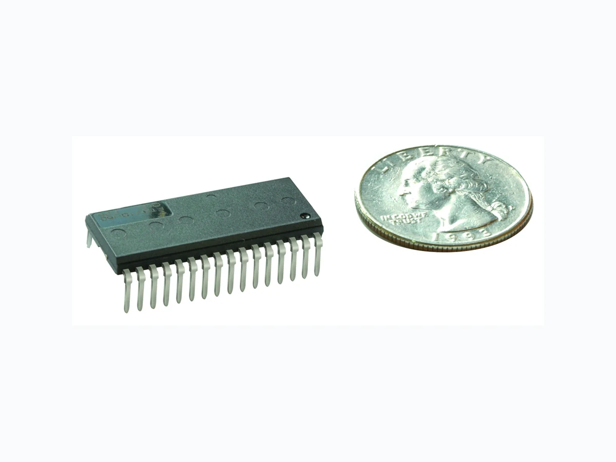
FSB50325 is a tiny smart power module (SPMTM) based on FRFET technology as a compact inverter solution for small power motor drive applications such as fan motors and water suppliers. It is composed of 6 fast-recovery MOSFET (FRFET), and 3 half-bridge HVICs for FRFET gate driving. FSB50325 provides low electromagnetic interference (EMI) characteristics with optimized switching speed. Moreover, since it employs FRFET as a power switch, it has much better ruggedness and larger safe operation area (SOA) than that of an IGBT-based power module or one-chip solution. The package is optimized for the thermal performance and compactness for the use in the built-in motor application and any other application where the
assembly space is concerned. FSB50325 is the most solution for the compact inverter providing the energy efficiency, compactness, and low electromagnetic interference.
Absolute Maximum Ratings
| Symbol | Parameter | Conditions | Rating | Units |
|---|---|---|---|---|
| V PN | DC Link Input Voltage, Drain-source Voltage of each FRFET | 250 | V | |
| I D25 | Each FRFET Drain Current, Continuous | T = 25°C C | 1.5 | A |
| I D80 | Each FRFET Drain Current, Continuous | T = 80°C C | 1.0 | A |
| I DP | Each FRFET Drain Current, Peak | T = 25°C, PW < 100µs C | 3.0 | A |
| P D | Maximum Power Dissipation | T = 80°C, Each FRFET C | 4.5 | W |
| V CC | Control Supply Voltage | Applied between V and COM CC | 20 | V |
| V BS | High-side Bias Voltage | Applied between V and V B S | 20 | V |
| V IN | Input Signal Voltage | Applied between IN and COM | -0.3 ~ VCC+0.3 | V |
| T J | Operating Junction Temperature | -20 ~ 125 | °C | |
| T STG | Storage Temperature | -50 ~ 150 | °C | |
| R θJC | Junction to Case Thermal Resistance | Each FRFET under inverter operating condition (Note 1) | 10.2 | °C/W |
| V ISO | Isolation Voltage | 60Hz, Sinusoidal, 1 minute, Connection pins to heatsink | 1500 | V rms |
©2005 Fairchild Semiconductor Corporation
Page 2
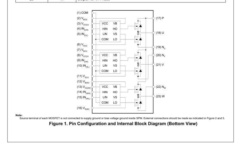
Pin Descriptions
| Pin Number | Pin Name | Pin Description |
|---|---|---|
| 1 | COM | IC Common Supply Ground |
| 2 | V B(U) | Bias Voltage for U Phase High Side FRFET Driving |
| 3 | V CC(U) | Bias Voltage for U Phase IC and Low Side FRFET Driving |
| 4 | IN (UH) | Signal Input for U Phase High-side |
| 5 | IN (UL) | Signal Input for U Phase Low-side |
| 6 | V S(U) | Bias Voltage Ground for U Phase High Side FRFET Driving |
| 7 | V B(V) | Bias Voltage for V Phase High Side FRFET Driving |
| 8 | V CC(V) | Bias Voltage for V Phase IC and Low Side FRFET Driving |
| 9 | IN (VH) | Signal Input for V Phase High-side |
| 10 | IN (VL) | Signal Input for V Phase Low-side |
| 11 | V S(V) | Bias Voltage Ground for V Phase High Side FRFET Driving |
| 12 | V B(W) | Bias Voltage for W Phase High Side FRFET Driving |
| 13 | V CC(W) | Bias Voltage for W Phase IC and Low Side FRFET Driving |
| 14 | IN (WH) | Signal Input for W Phase High-side |
| 15 | IN (WL) | Signal Input for W Phase Low-side |
| 16 | V S(W) | Bias Voltage Ground for W Phase High Side FRFET Driving |
| 17 | P | Positive DC–Link Input |
| 18 | U | Output for U Phase |
| 19 | N U | Negative DC–Link Input for U Phase |
| 20 | N V | Negative DC–Link Input for V Phase |
| 21 | V | Output for V Phase |
| 22 | N W | Negative DC–Link Input for W Phase |
| 23 | W | Output for W Phase |
Page 3
Electrical Characteristics (TJ = 25°C, VCC=VBS=15V Unless Otherwise Specified)
Inverter Part (Each FRFET Unless Otherwise Specified)
| Symbol | Parameter | Conditions | Min | Typ | Max | Units |
|---|---|---|---|---|---|---|
| BV DSS | Drain-Source Breakdown Voltage | V = 0V, I = 250µA (Note 2) IN D | 250 | - | - | V |
| ∆BV DSS/ ∆T J | Breakdown Voltage Tem- perature Coefficient | I = 250µA, Referenced to 25°C D | - | 0.31 | - | V/°C |
| I DSS | Zero Gate Voltage Drain Current | V = 0V, V = 250V IN DS | - | - | 250 | µA |
| R DS(on) | Static Drain-Source On-Resistance | V = V = 15V, V = 5V, I = 1.0A CC BS IN D | - | 1.4 | 1.8 | Ω |
| V SD | Drain-Source Diode Forward Voltage | V = V = 15V, V = 0V, I = -1.0A CC BS IN D | - | - | 1.2 | V |
| t ON | Switching Times | V = 150V, V = V = 15V, I = 1.0A PN CC BS D V = 0V ↔ 5V, R = 0Ω IN EH Inductive load L=3mH High- and low-side FRFET switching (Note 3) | - | 1076 | - | ns |
| t OFF | - | 660 | - | ns | ||
| t rr | - | 108 | - | ns | ||
| E ON | - | 47 | - | µJ | ||
| E OFF | - | 3.1 | - | µJ | ||
| RBSOA | Reverse-bias Safe Oper- ating Area | V = 200V, V = V = 15V, I = I , R = 0Ω PN CC BS D DP EH V =BV , T = 125°C DS DSS J High- and low-side FRFET switching (Note 4) | Full Square | |||
Control Part (Each HVIC Unless Otherwise Specified)
| Symbol | Parameter | Conditions | Min | Typ | Max | Units | |
|---|---|---|---|---|---|---|---|
| I QCC | Quiescent V Current CC | V =15V, V =0V CC IN | Applied between V and COM CC | - | - | 160 | µA |
| I QBS | Quiescent V Current BS | V =15V, V =0V BS IN | Applied between V and V B S | - | - | 100 | µA |
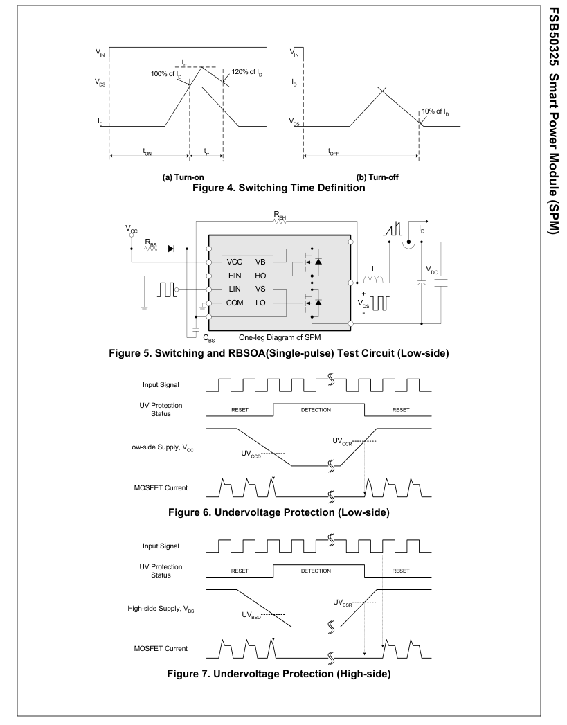
| UV CCD | Low-side Undervoltage Protection (Figure 6) | V Undervoltage Protection Detection Level CC | 7.4 | 8.0 | 9.4 | V | |
| UV CCR | V Undervoltage Protection Reset Level CC | 8.0 | 8.9 | 9.8 | V | ||
| UV BSD | High-side Undervoltage Protection (Figure 7) | V Undervoltage Protection Detection Level BS | 7.4 | 8.0 | 9.4 | V | |
| UV BSR | V Undervoltage Protection Reset Level BS | 8.0 | 8.9 | 9.8 | V | ||
| V IH | ON Threshold Voltage | Logic High Level | Applied between IN and COM | 3.0 | - | - | V |
| V IL | OFF Threshold Voltage | Logic Low Level | - | - | 0.8 | V | |
| I IH | Input Bias Current | V = 5V IN | Applied between IN and COM | - | 10 | 20 | µA |
| I IL | V = 0V IN | - | - | 2 | µA | ||
Note: 1. For the measurement point of case temperature TC, please refer to Figure 3 in page 4. 2. BVDSS is the absolute maximum voltage rating between drain and source terminal of each FRFET inside SPM. VPN should be sufficiently less than this value considering the effect of the stray inductance so that VDS should not exceed BVDSS in any case. 3. tON and tOFF include the propagation delay time of the internal drive IC. Listed values are measured at the laboratory test condition, and they can be different according to the field applcations due to the effect of different printed circuit boards and wirings. Please see Figure 4 for the switching time definition with the switching test circuit of Figure 5.
- The peak current and voltage of each FRFET during the switching operation should be included in the safe operating area (SOA). Please see Figure 5 for the RBSOA test circuit that is same as the switching test circuit.
Page 4
Recommended Operating Conditions
| Symbol | Parameter | Conditions | Value | Units | ||
|---|---|---|---|---|---|---|
| Min. | Typ. | Max. | ||||
| V PN | Supply Voltage Applied betwee | n P and N | - | 150 | 200 | V |
| V CC | Control Supply Voltage Applied betwee | n V and COM CC | 13.5 | 15 | 16.5 | V |
| V BS | High-side Bias Voltage Applied betwee | n V and V B S | 13.5 | 15 | 16.5 | V |
| V IN(ON) | Input ON Threshold Voltage Applied betwee Input OFF Threshold Voltage | n IN and COM | 3.0 | V CC | V | |
| V IN(OFF) | 0 | 0.6 | V | |||
| t dead | Blanking Time for Preventing V =V =13.5 Arm-short CC BS | ~ 16.5V, T ≤ 125°C J | 1.0 | - | - | µs |
| f PWM | PWM Switching Frequency T ≤ 125°C J | - | 15 | - | kHz | |
| T C | Case Temperature T J ≤ 125°C | -20 | 100 | °C | ||
These values depend on PWM control algorithm
R2
15-V Line
| HIN | LIN | Output | Note |
| 0 | 0 | Z | Both FRFET Off |
| 0 | 1 | 0 | Low-side FRFET On |
| 1 | 0 | V DC | High-side FRFET On |
| 1 | 1 | Forbidden | Shoot-through |
| Open | Open | Z | Same as (0, 0) |
VDC P
R1 D1
VCC VB
Inverter
R5
Output
HIN HO
Micom
LIN VS
C3
C5
COM LO
R3 N
One-Leg Diagram of SPM
C2 C1
10µF
\* Example of bootstrap paramters: C1 = C2 = 1µF ceramic capacitor, R1 = 56Ω, R2 = 20Ω
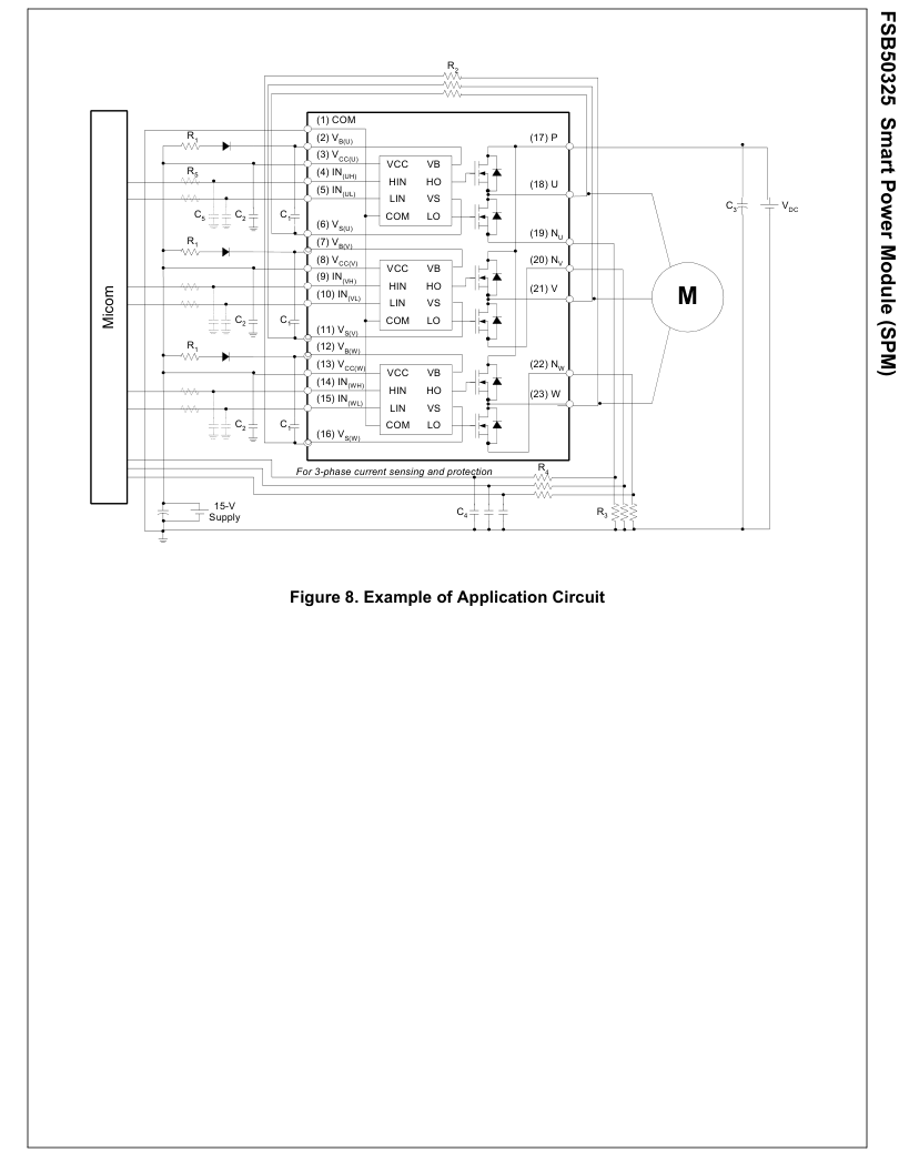
Note: (1) It is recommended the bootstrap diode D1 to have soft and fast recovery characteristics with 600-V rating (2) Parameters for bootsrap circuit elements are dependent on PWM algorithm. For 15 kHz of switching frequency, typical example of parameters is shown above. (3) RC coupling(R5 and C5) at each input (indicated as dotted lines) may be used to prevent improper input signal due to surge noise. Signal input of SPM is compatible with standard CMOS or LSTTL outptus. (4) Bold lines should be short and thick in PCB pattern to have small stray inductance of circuit, which results in the reduction of surge voltage. Bypass capacitors such as C1, C2
and C3 should have good high-frequency characteristics to absorb high-frequency ripple current.
Figure 2. Recommended CPU Interface and Bootstrap Circuit with Parameters
14.50mm
3.80mm
Case Temperature (TC)
MOSFET
Detecting Point
Note: Attach the thermocouple on top of the heatsink-side of SPM (between SPM and heatsink if applied) to get the correct temperature measurement.
Figure 3. Case Temperature Measurement
Page 5
Page 6
Page 7
Page 8
TRADEMARKS
The following are registered and unregistered trademarks Fairchild Semiconductor owns or is authorized to use and is not intended to be an exhaustive list of all such trademarks.
FAST®
ACEx™
POP™
IntelliMAX™
SPM™
Power247™
FASTr™
ISOPLANAR™
Stealth™
ActiveArray™
PowerEdge™
FPS™
LittleFET™
SuperFET™
Bottomless™
MICROCOUPLER™
FRFET™
CoolFET™
GlobalOptoisolator™
MicroFET™
CROSSVOLT™
GTO™
MicroPak™
DOME™
HiSeC™
MICROWIRE™
EcoSPARK™
I2C™
MSX™
E2CMOS™
i-Lo™
MSXPro™
EnSigna™
ImpliedDisconnect™
OCX™
FACT™
OCXPro™
FACT Quiet Series™
OPTOLOGIC®
Across the board. Around the world.™
PowerSaver™
SuperSOT™-3
PowerTrench®
SuperSOT™-6
QFET®
SuperSOT™-8
QS™
SyncFET™ TinyLogic®
QT Optoelectronics™ Quiet Series™
TINYOPTO™
RapidConfigure™
TruTranslation™
RapidConnect™
UHC™ UltraFET®
µSerDes™
OPTOPLANAR™
SILENT SWITCHER®
UniFET™
The Power Franchise®
PACMAN™
SMART START™
VCX™
Programmable Active Droop™
DISCLAIMER
FAIRCHILD SEMICONDUCTOR RESERVES THE RIGHT TO MAKE CHANGES WITHOUT FURTHER NOTICE TO ANY PRODUCTS HEREIN TO IMPROVE RELIABILITY, FUNCTION OR DESIGN. FAIRCHILD DOES NOT ASSUME ANY LIABILITY ARISING OUT OF THE APPLICATION OR USE OF ANY PRODUCT OR CIRCUIT DESCRIBED HEREIN; NEITHER DOES IT CONVEY ANY LICENSE UNDER ITS PATENT RIGHTS, NOR THE RIGHTS OF OTHERS.
LIFE SUPPORT POLICY
FAIRCHILD’S PRODUCTS ARE NOT AUTHORIZED FOR USE AS CRITICAL COMPONENTS IN LIFE SUPPORT DEVICES OR SYSTEMS WITHOUT THE EXPRESS WRITTEN APPROVAL OF FAIRCHILD SEMICONDUCTOR CORPORATION. As used herein:
- Life support devices or systems are devices or systems which, (a) are intended for surgical implant into the body, or (b) support or sustain life, or (c) whose failure to perform when properly used in accordance with instructions for use provided in the labeling, can be reasonably expected to result in significant injury to the user.
PRODUCT STATUS DEFINITIONS
Definition of Terms
- A critical component is any component of a life support device or system whose failure to perform can be reasonably expected to cause the failure of the life support device or system, or to affect its safety or effectiveness.
| Datasheet Identification | Product Status | Definition |
| Advance Information | Formative or In Design | This datasheet contains the design specifications for product development. Specifications may change in any manner without notice. |
| Preliminary | First Production | This datasheet contains preliminary data, and supplementary data will be published at a later date. Fairchild Semiconductor reserves the right to make changes at any time without notice in order to improve design. |
| No Identification Needed | Full Production | This datasheet contains final specifications. Fairchild Semiconductor reserves the right to make changes at any time without notice in order to improve design. |
| Obsolete | Not In Production | This datasheet contains specifications on a product that has been discontinued by Fairchild semiconductor. The datasheet is printed for reference information only. |
Rev. I15