


 Download PDF
FSA1256 FAIRCHILD
Document overview
- PDF pages: 9
Technical content
Page 1
| March 2004 Revised January 2005 FSA1256 • FSA1257 • FSA1258 Low R Low Voltage Dual SPST Analog Switch ON General Description Features The FSA1256, FSA1257, and FSA1258 are high perfor- I Maximum 1.1Ω On Resistance (RON) for 4.5V supply m swa in tcc he sd u Ta hl eS sein g dl ee icP eo sle / fS eain tg ul re uT lh trr ao w w(S P RS OT ) oa n 1a .1lo Ωg I 0.4Ω max RON flatness for 4.5V supply e . v e lo N f I Space saving Pb-Free MicroPak packaging maximum at 4.5V VCC and will operate over the wide VCC range of 1.65V to 5.5V. These devices are fabricated with I Broad VCC operating range: 1.65V to 5.5V sub-micron CMOS technology to achieve fast switching I Fast turn-on and turn-off time speeds and are designed for break-before-make operation. I FSA1258 features break-before-make enable circuitry The select input is TTL level compatible. The FSA1256 fea- I Over-voltage tolerant TTL compatible control input tures two Normally Open (NO) switches. The FSA1257 features two Normally Closed (NC) switches. The FSA1258 has one NO switch and one NC switch. | ||||
|---|---|---|---|---|
| Ordering Code: | ||||
| Order Number | Package Number | Product Code Top Mark | Package Description | Supplied As |
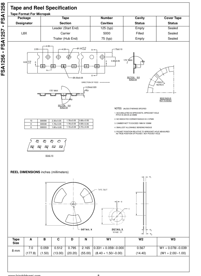
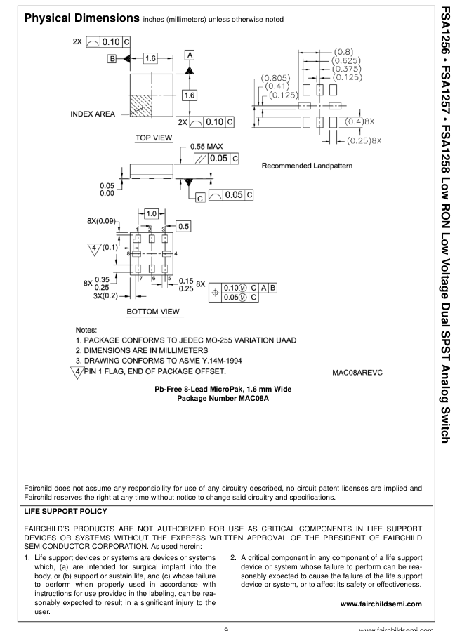
| FSA1256L8X | MAC08A | EB | Pb-Free 8-Lead MicroPak, 1.6 mm Wide | 5K Units on Tape and Reel |
| FSA1257L8X | MAC08A | EC | Pb-Free 8-Lead MicroPak, 1.6 mm Wide | 5K Units on Tape and Reel |
| FSA1258L8X | MAC08A | ED | Pb-Free 8-Lead MicroPak, 1.6 mm Wide | 5K Units on Tape and Reel |
| Pb-Free package per JEDEC J-STD-020B. Analog Symbols FSA1256 FSA1257 (Top Through View) (Top Through View) Truth Tables FSA1256 FSA1257 Control Input(s) Function Control Input(s) Function L Disconnect L A Connected to B H A Connected to B H Disconnect H = HIGH Logic Level L = LOW Logic Level MicroPak is a trademark of Fairchild Semiconductor Corporation. | ||||
| Control Input(s) | Function |
| L | Disconnect |
| H | A Connected to B |
| Control Input(s) | Function |
| L | A Connected to B |
| H | Disconnect |
© 2005 Fairchild Semiconductor Corporation
DS500883
www.fairchildsemi.com
Page 2
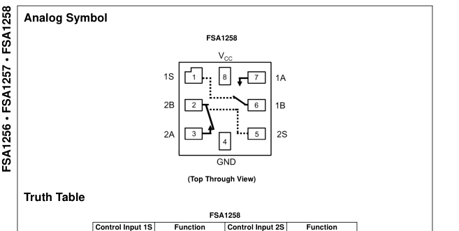
| Control Input 1S | Function | Control Input 2S | Function |
| L | 1A Connected to 1B | L | Disconnect |
| H | Disconnect | H | 2A Connected to 2B |
H = HIGH Logic Level L = LOW Logic Level
Pin Descriptions
| Pin Names | Function |
| A, B | Data Ports |
| S | Control Input |
www.fairchildsemi.com
2
Page 3
| Absolute Maximum Ratings Recommended Operating (Note 1) Conditions Supply Voltage (VCC) −0.5V to +6.0V Switch Voltage (VS) (Note 2) −0.5V to VCC + 0.5V Supply Voltage (VCC) 1.65V to 5.5V Input Voltage (VIN) (Note 2) −0.5V to +6.0V Control Input Voltage (VIN) (Note 3) 0V to VCC Input Diode Current −50 mA Switch Input Voltage (VIN) 0V to VCC Switch Current 200 mA Operating Temperature (TA) −40°C to +85°C Peak Switch Current (Pulsed at Thermal Resistance (θJA) in still air 1 ms duration, <10% Duty Cycle) 400 mA MicroPak 8L package 224°C/W Power Dissipation @ 85°C (modeled) MicroPak 8L package 180 mW Storage Temperature Range (TSTG) −65°C to +150°C Note 1: The “Absolute Maximum Ratings” are those values beyond which the safety of the device cannot be guaranteed. The device should not be Maximum Junction Temperature (TJ) +150°C operated at these limits. The parametric values defined in the Electrical Lead Temperature (TL) Characteristics tables are not guaranteed at the absolute maximum ratings. The “Recommended Operating Conditions” table will define the conditions Soldering, 10 seconds +260°C for actual device operation. ESD Note 2: The input and output negative voltage ratings may be exceeded if the input and output diode current ratings are observed. Human Body Model 5.5kV Note 3: Unused inputs must be held HIGH or LOW. They may not float. DC Electrical Characteristics (All typical values are @ 25°C unless otherwise specified) | ||||||
|---|---|---|---|---|---|---|
| Symbol | Parameter | VCC (V) | TA = +25°C | TA= −40°C to +85°C | Units | Conditions |
| Min Typ Max | Min Max | |||||
| VIH | Input Voltage High | 2.7 to 3.6 | 2.0 | V | ||
| 4.5 to 5.5 | 2.4 | |||||
| VIL | Input Voltage Low | 2.7 to 3.6 | 0.6 | V | ||
| 4.5 to 5.5 | 0.8 | |||||
| IIN | Control Input Leakage | 2.7 to 3.6 | −1.0 1.0 | µA | VIN = 0V to VCC | |
| 4.5 to 5.5 | −1.0 1.0 | |||||
| INO(OFF), INC(OFF) | OFF-Leakage Current | 5.5 | -2.0 2.0 | −20.0 20.0 | nA | A = 1V, 4.5V 1B or 2B = 1V, 4.5V |
| RON | Switch On Resistance (Note 4) | 2.7 | 2.6 4.0 | 4.3 | Ω | IOUT = 100 mA, 1B or 2B = 1.5V |
| 4.5 | 0.95 1.18 | 1.3 | IOUT = 100 mA, 1B or 2B = 3.5V | |||
| ∆RON | On Resistance Matching Between Channels (Note 5) | 4.5 | 0.06 0.12 | 0.15 | Ω | IOUT = 100 mA, 1B or 2B = 3.5V |
| RFLAT(ON) | On Resistance Flatness (Note 6) | 2.7 | 1.4 | Ω | IOUT = 100 mA, 1B or 2B = 0V, 0.75V, 1.5V | |
| 4.5 | 0.2 0.3 | 0.4 | IOUT = 100 mA, 1B or 2B = 0V, 1V, 2V | |||
| ICC | Quiescent Supply Current | 3.6 | 0.1 0.5 | 1.0 | µA | VIN = 0V or VCC, IOUT = 0V |
| 5.5 | 0.1 0.5 | 1.0 | ||||
| Note 4: On Resistance is determined by the voltage drop between A and B pins at the indicated current through the switch. Note 5: ∆RON = RONmax − RONmin measured at identical VCC, temperature, and voltage. Note 6: Flatness is defined as the difference between the maximum and minimum value of On Resistance over the specified range of conditions. | ||||||
3
www.fairchildsemi.com
Page 4
www.fairchildsemi.com
4
Page 5
5
www.fairchildsemi.com
Page 6
www.fairchildsemi.com
6
Page 7
7
www.fairchildsemi.com
Page 8
www.fairchildsemi.com
8
Page 9
9
www.fairchildsemi.com