


 Download PDF
FM50 FAIRCHILD
Document overview
- PDF pages: 8
Technical content
Page 1
www.fairchildsemi.com

Features
- Analog output: 10 mV/°C
- Range: -40 to 125°C range:
- Accuracy: ±1°C at 25°C
- Supply Current, 170 µA max.
- Output Drive, 25 µA
- Self-heating < 0.1°C
- Operating Voltage: +2.4V to +6V
Applications
- Mobile Phones
- Computers
- Battery Management
- Office Equipment
- HVAC
- Power Supply Modules
- Disk Drives
- Automotive
Thermal Response
Description
As a precision CMOS temperature sensor, the FM50 is cost-effective for accurate low-power temperature monitoring applications. Output voltage versus temperature is extremely linear. With no load, the supply current is typically 130µA. For normal operation, the load on VOUT
Ω
should be 100K or less.
In a typical application, a remotely mounted FM50 is monitored by a microcontroller with an analog A/D converter input. Alternatively, the FM50 can drive a comparator with a high impedance input.
Accuracy is typically ± 0.5°C at room temperature; and better than ±2°C from 0 to 75°C.
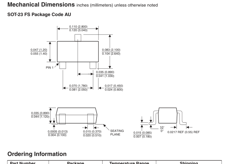
Package is a 3-pin SOT-23
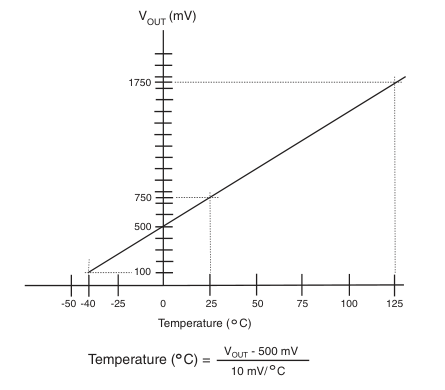
FM50 Output Voltage vs. Temperature
Page 2
Pin Assignments
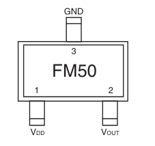
Pin Descriptions
| Pin Name | Pin No. | Type | Function |
|---|---|---|---|
| VOUT | 2 | Analog Output | Temperature Sense. Analog output voltage indicating temperature. VOUT = 500+10T(°C) mV |
| VDD | 1 | Power | Supply Voltage. 2.4 to 6.0V |
| GND | 3 | Power | Ground. |
Page 3
1
Absolute Maximum Ratings
Parameter
Min.
Typ.
Max. Units
Supply Voltage
+7 V
V + 0.5
V
Output Voltage
DD
Output Current
10 µA
2
Operating Temperature Range
-50
+150
°C
Storage Temperature Range
-60
+150
°C
Lead Soldering Temperature
220 °C
2 ESD Human Body Model
2000
V
Machine Model
250
V
Notes: 1. Absolute maximum ratings are limits beyond which operation may cause permanent damage to the device. These are stress ratings only; functional operation at or above these limits is not implied. 2. Operating ratings are conditions for which the device is intended to be functional without specific guaranteed performance limits. For guaranteed specifications and test conditions refer to Electrical Characteristics. 3. Human Body Model: 100pF capacitor discharged through a 1.5kOhm resistor into each pin. Machine Model: 200pF capacitor discharged directly into each pin.
4
Electrical Characteristics
Limits apply for -40°C T +125°C and V = +5.0V unless otherwise noted.
≤ A ≤
DD
Parameter
Symbol
Conditions
Min Typ Max Units
Transfer Characteristic Sensitivity
A
9.7 10 10.3 mV/°C
OUT
Output at 25°C
740 750 760 mV
5 Accuracy
T = +25°C
-1 ±0.5 +1 °C
A T = -40°C (T )
-3.5 ±1 +3.5 °C
A
MIN
TA= +125°C (TMAX)
-3 ±1 +3 °C
Temperature Range
-40
+125 °C
6
Non-Linearity
-0.8
+0.8 °C
Output Output Voltage Range
100
1500 mV
Output Current Source
I Sensing
25
µA
ONSN I Surge
mA
ONSG
Output Current Sink
I
50
µA
OL 100kΩload at 25°C
kΩ
Output resistance
1
10
Load regulation
mV/mA
Power Supply Voltage
V
2.4
6.0 V
DD
Quiescent Current
IS No output load
170 µA
Package Thermal Resistance
260
°C/W
Notes: 4. These specifications are guaranteed only for the test conditions listed. 5. Accuracy (expressed in °C) = Difference between calculated output voltage and measured output voltage. Calculated output voltage = 10mV/°C multiplied by the device’s case temperature at specified conditions of temperature, voltage and power supply, added to 500mV. 6. Non-linearity is defined as the deviation of the output-voltage-versus-temperature curve from the best-fit straight line, over the device’s rated temperature range.
Page 4
Typical Performance Characteristics
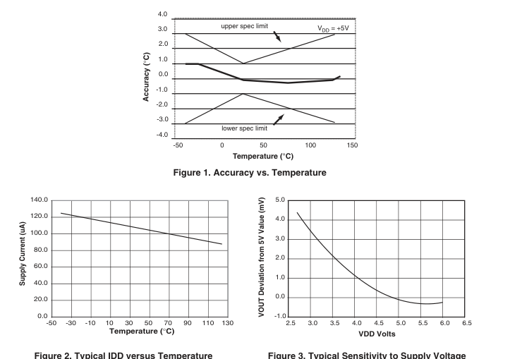
Description
Within the FM50 are a thermal diode, calibration circuits and amplifiers. Since the FM50 is calibrated at 33°C, the nominal output in mV is:
- 33 ( )
VOUT = 830 + 10 T –
where T is the thermal junction temperature expressed in °C.
At 33°C, the tolerances are as follows:
- Offset is ±3mV
- Slope, ±0.3mV/°C
These values accommodate the specified accuracies at -40, 25 and +125°C.
Output structure of the FM50 is an n-channel CMOS transistor driving a p-channel load. Available current is typically 50
Ω
µA to ground. Series resistance is typically 7 k , charging and 2 kΩ, discharging through a capacitor connected from V to ground. OUT
Following application of power to V , V is accurate
DD OUT
following a delay of approximately 80 msec.
Page 5
Applications Information
Although the FM50 is a simple device, care must be taken to ensure that temperature is measured accurately. There are two major sources of errors:
- Voltage errors.
- Thermal Delay Errors.
- Location errors
Voltage Errors
VDD
VOUT
GND(power)
GND(sense)
Figure 4. Recommended Electrical Connections
A Kelvin connection is recommended to avoid errors due to voltage drops in the ground connections. Although the typical 130µA supply current draw of the FM50 will only cause a 130µV error if the series resistance is 1Ω, a 100 mA current supply to adjacent circuits can cause a 10mV drop Ω Ω
across 100m (10m is a typical value for soldered joints or contact resistance), leading to a 1°C error. For this reason, the FM50 should be Kelvin connected as shown in Figure 4.
Thermal Delay Errors For measurement accuracy of the order of tenths of 1°C, adequate settling time must be allowed. For a typical circuit board installation, 15 minutes should be allowed to elapse following reading of temperature within 1 - 2°C of the expected final value. Once V has ceased to slew and
OUT
is stable (with or without about ±0.1°C noise) for about 5 minutes, temperature can be calculated.
Location Errors Position is another source of error. Even within a controlled thermal environment, changing location by a few inches can lead to errors of several tenths of 1°C
Mounting The FM50 can be easily mounted by gluing or cementing it to a surface. In this case, its temperature will be within about 0.2°C of the temperature of the surface it is attached to if the ambient air temperature is almost the same as the surface temperature. If the air temperature is much higher or lower than the surface temperature, the actual temperature of the FM50 die will be at an intermediate temperature between the surface temperature and the air temperature.
To ensure good thermal conductivity, the backside of the FM50 die is directly attached to the GND pin. The lands and traces to the FM50 will, of course, be part of the printed circuit board, which is the object whose temperature is being measured. These printed circuit board lands and traces will not cause the FM50’s temperature to deviate from the desired temperature.
Alternatively, the FM50 can be mounted inside a sealed-end metal tube, and can then be dipped into a bath or screwed into a threaded hole in a tank. As with any IC, the FM50 and accompanying wiring and circuits must be kept insulated and dry to avoid leakage and corrosion. This is especially true if the circuit may operate at cold temperatures where condensation can occur. Printed-circuit coatings and varnishes such as Humiseal and epoxy paint or dips can be used to ensure that moisture cannot corrode the FM50 or its connections.
Page 6
Typical Applications Circuits
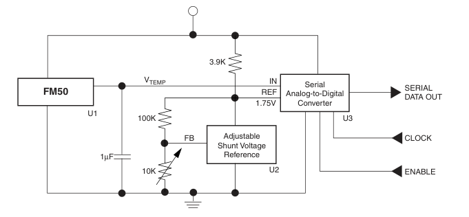
Figure 4. Serial Output Temperature to Digital Converter (Full Scale = +125°C)
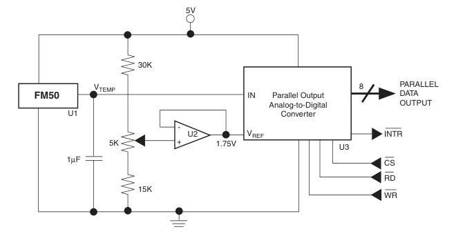
Figure 5. Parallel Output Temperature to Digital Converter (Full Scale = +125°C)
Page 7
Page 8
| Part Number | Package | Temperature Range | Shipping |
|---|---|---|---|
| FM50S3X | 3-Pin SOT-23 | -40°C to +125°C | Tape and Reel, 3000 units/reel |


LIFE SUPPORT POLICY
FAIRCHILD’S PRODUCTS ARE NOT AUTHORIZED FOR USE AS CRITICAL COMPONENTS IN LIFE SUPPORT DEVICES OR SYSTEMS WITHOUT THE EXPRESS WRITTEN APPROVAL OF THE PRESIDENT OF FAIRCHILD SEMICONDUCTOR CORPORATION. As used herein:
- Life support devices or systems are devices or systems which, (a) are intended for surgical implant into the body, or (b) support or sustain life, and (c) whose failure to perform when properly used in accordance with instructions for use provided in the labeling, can be reasonably expected to result in a significant injury of the user.
www.fairchildsemi.com
- A critical component in any component of a life support device or system whose failure to perform can be reasonably expected to cause the failure of the life support device or system, or to affect its safety or effectiveness.
9/12/02 0.0m 003 Stock#DS30000050
2002 Fairchild Semiconductor Corporation