


 Download PDF
Technical datasheet
Document overview
- PDF pages: 18
Technical content
Page 1
Supercapacitors
FM Series
Overview
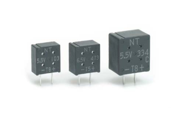
FM Series Supercapacitors, also known as Electric Double- Layer Capacitors (EDLCs), are intended for high energy storage applications.
Benefits
- Rectangular case
- Wide range of temperature from −25°C to +70°C (all types
except FMR) and −40°C to +85°C (FMR type)
- Maintenance free
- 3.5 VDC, 5.5 VDC, and 6.5 VDC
- Highly reliable against liquid leakage
- Lead-free and RoHS Compliant
- Leads can be transverse mounted
Part Number System
Applications
Supercapacitors have characteristics ranging from traditional capacitors and batteries. As a result, supercapacitors can be used like a secondary battery when applied in a DC circuit. These devices are best suited
for use in low voltage DC hold-up applications such as embedded microprocessor systems with flash memory.
| FM | 0H | 223 | Z | F | TP | 16 |
| Series | Maximum Operating Voltage | Capacitance Code (F) | Capacitance Tolerance | Environmental | Tape Type | Height (excluding lead) |
| FM FME FML FMR FMC | 0V = 3.5 VDC 0H = 5.5 VDC 0J = 6.5 VDC | First two digits represent significant figures. Third digit specifies number of zeros. | Z = −20/+80% | F = Lead-free | TP = AMMO L1 = Transverse mounting Blank = Bulk | 16 = 16 mm 18 = 18 mm Blank = Bulk |
One world. One KEMET
Page 2
Dimensions – Millimeters
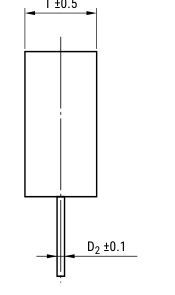
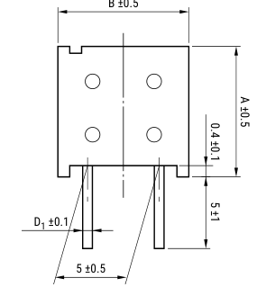
| Part Number | A | B | T | D 1 | D 2 |
|---|---|---|---|---|---|
| FM0H103ZF | 11.5 | 10.5 | 5.0 | 0.5 | 0.4 |
| FM0H223ZF | 11.5 | 10.5 | 5.0 | 0.5 | 0.4 |
| FM0H473ZF | 11.5 | 10.5 | 5.0 | 0.5 | 0.4 |
| FM0H104ZF | 11.5 | 10.5 | 6.5 | 0.5 | 0.4 |
| FM0H224ZF | 11.5 | 10.5 | 6.5 | 0.5 | 0.4 |
| FM0V473ZF | 11.5 | 10.5 | 5.0 | 0.5 | 0.4 |
| FM0V104ZF | 11.5 | 10.5 | 5.0 | 0.5 | 0.4 |
| FM0V224ZF | 11.5 | 10.5 | 6.5 | 0.5 | 0.4 |
| FM0J473ZF | 11.5 | 10.5 | 6.5 | 0.5 | 0.4 |
| FME0H223ZF | 11.5 | 10.5 | 5.0 | 0.5 | 0.4 |
| FME0H473ZF | 11.5 | 10.5 | 5.0 | 0.5 | 0.4 |
| FML0H333ZF | 11.5 | 10.5 | 5.0 | 0.5 | 0.4 |
| FMR0H473ZF | 11.5 | 10.5 | 6.5 | 0.5 | 0.4 |
| FMR0H104ZF | 11.5 | 10.5 | 6.5 | 0.5 | 0.4 |
| FMR0V104ZF | 11.5 | 10.5 | 6.5 | 0.5 | 0.4 |
| FMC0H473ZF | 11.5 | 10.5 | 5.0 | 0.5 | 0.4 |
| FMC0H104ZF | 11.5 | 10.5 | 6.5 | 0.5 | 0.4 |
| FMC0H334ZF | 15.0 | 14.0 | 9.0 | 0.6 | 0.6 |
Lead Terminal Forming
For transverse mounting <L1>
Add “L1” to the end of bulk part number for transverse mounting option
Page 3
Performance Characteristics
Supercapacitors should not be used for applications such as ripple absorption because of their high internal resistance
(several hundred mΩ to a hundred Ω) compared to aluminum electrolytic capacitors. Thus, its main use would be
similar to that of secondary battery such as power back-up in DC circuit. The following list shows the characteristics of
supercapacitors as compared to aluminum electrolytic capacitors for power back-up and secondary batteries.
| Secondary Battery | Capacitor | |||
| NiCd | Lithium Ion | Aluminum Electrolytic | Supercapacitor | |
| Back-up ability | – | – | – | – |
| Eco-hazard | Cd | – | – | – |
| Operating Temperature Range | −20 to +60°C | −20 to +50°C | −55 to +105°C | −40 to +85°C (FR, FT) |
| Charge Time | few hours | few hours | few seconds | few seconds |
| Charge/Discharge Life Time | approximately 500 times | approximately 500 to 1,000 times | limitless (*1) | limitless (*1) |
| Restrictions on Charge/Discharge | yes | yes | none | none |
| Flow Soldering | not applicable | not applicable | applicable | applicable |
| Automatic Mounting | not applicable | not applicable | applicable | applicable (FM and FC series) |
| Safety Risks | leakage, explosion | leakage, combustion, explosion, ignition | heat-up, explosion | gas emission (*2) |
(\*1) Aluminum electrolytic capacitors and supercapacitors have limited lifetime. However, when used under proper conditions, both can operate within a predetermined lifetime. (\*2) There is no harm as it is a mere leak of water vapor which transitioned from water contained in the electrolyte (diluted sulfuric acid). However, application of abnormal voltage surge exceeding maximum operating voltage may result in leakage and explosion.
Typical Applications
| Intended Use (Guideline) | Power Supply (Guideline) | Application | Examples of Equipment | Series |
| Long time back-up | 500 μA and below | CMOS microcomputer, IC for clocks | CMOS microcomputer, static RAM/DTS (digital tuning system) | FM series |
Environmental Compliance
All KEMET supercapacitors are RoHS Compliant.
RoHS Compliant
Page 4
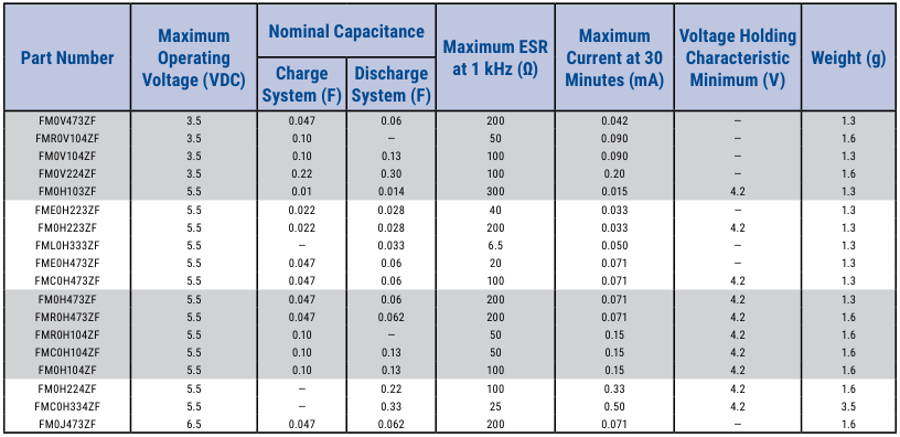
Table 1 – Ratings & Part Number Reference
Page 5
Specifications – All Types Except FMR
| Item | FM 5.5 V Type, 3.5 V Type, 6.5 V Type, FMC Type | FML Type, FME Type | Test Conditions (conforming to JIS C 5160-1) | |||
|---|---|---|---|---|---|---|
| Category Temperature Range | −25°C to +70°C | −25°C to +70°C | ||||
| Maximum Operating Voltage | 5.5 VDC, 3.5 VDC, 6.5 VDC | 5.5 VDC | ||||
| Capacitance | Refer to Table 1 | Refer to Table 1 | Refer to “Measurement Conditions” | |||
| Capacitance Allowance | +80%, −20% | +80%, −20% | Refer to “Measurement Conditions” | |||
| ESR | Refer to Table 1 | Refer to Table 1 | Measured at 1 kHz, 10 mA; See also “Measurement Conditions” | |||
| Current (30 minutes value) | Refer to Table 1 | Refer to Table 1 | Refer to “Measurement Conditions” | |||
| Surge | Capacitance | > 90% of initial ratings | > 90% of initial ratings | Surge voltage: 4.0 V (3.5 V type) 6.3 V (5.5 V type) 7.4 V (6.5 V type) Charge: 30 seconds Discharge: 9 minutes 30 seconds Number of cycles: 1,000 Series resistance: 0.010 F 1500 Ω 0.022 F 560 Ω 0.033 F 510 Ω 0.047 F 300 Ω 0.068 F 240 Ω 0.10 F 150 Ω 0.22 F 56 Ω Discharge 0.33 F 51 Ω resistance: Temperature: 0 Ω 70±2°C | ||
| ESR | ≤ 120% of initial ratings | ≤ 120% of initial ratings | ||||
| Current (30 minutes value) | ≤ 120% of initial ratings | ≤ 120% of initial ratings | ||||
| Appearance | No obvious abnormality | No obvious abnormality | ||||
| Characteristics in Different Temperature | Capacitance | Phase 2 | ≥ 50% of initial value | Phase 2 | ≥ 50% of initial value | Conforms to 4.17 Phase 1: +25±2°C Phase 2: −25±2°C Phase 4: +25±2°C Phase 5: +70±2°C Phase 6: +25±2°C |
| ESR | ≤ 400% of initial value | ≤ 400% or less than initial value | ||||
| Capacitance | Phase 3 | Phase 3 | ||||
| ESR | ||||||
| Capacitance | Phase 5 | ≤ 200% of initial value | Phase 5 | ≤ 200% of initial value | ||
| ESR | Satisfy initial ratings | Satisfy initial ratings | ||||
| Current (30 minutes value) | ≤ 1.5 CV (mA) | ≤ 1.5 CV (mA) | ||||
| Capacitance | Phase 6 | Within ±20% of initial value | Phase 6 | Within ±20% of initial value | ||
| ESR | Satisfy initial ratings | Satisfy initial ratings | ||||
| Current (30 minutes value) | Satisfy initial ratings | Satisfy initial ratings | ||||
| Vibration Resistance | Capacitance | Satisfy initial ratings | Satisfy initial ratings | Conforms to 4.13 Frequency: 10 to 55 Hz Testing Time: 6 hours | ||
| ESR | ||||||
| Current (30 minutes value) | ||||||
| Appearance | No obvious abnormality | No obvious abnormality | ||||
| Solderability | Over 3/4 of the terminal should be covered by the new solder | Over 3/4 of the terminal should be covered by the new solder | Conforms to 4.11 Solder temp: +245±5°C Dipping time: 5±0.5 seconds 1.6 mm from the bottom should be dipped. | |||
Page 6
Specifications – All Types Except FMR cont’d
| Item | FM 5.5 V Type, 3.5 V Type, 6.5 V Type, FMC Type | FML Type, FME Type | Test Conditions (conforming to JIS C 5160-1) | |
|---|---|---|---|---|
| Solder Heat Resistance | Capacitance | Satisfy initial ratings | Satisfy initial ratings | Conforms to 4.10 Solder temp: +260±10°C Dipping time: 10±1 seconds 1.6 mm from the bottom should be dipped. |
| ESR | ||||
| Current (30 minutes value) | ||||
| Appearance | No obvious abnormality | No obvious abnormality | ||
| Temperature Cycle | Capacitance | Satisfy initial ratings | Satisfy initial ratings | Conforms to 4.12 Temperature Condition: −25°C » Room temperature » +70°C » Room temperature Number of cycles: 5 cycles |
| ESR | ||||
| Current (30 minutes value) | ||||
| Appearance | No obvious abnormality | No obvious abnormality | ||
| High Temperature and High Humidity Resistance | Capacitance | Within ±20% of initial value | Within ±20% of initial value | Conforms to 4.14 Temperature: +40±2°C Relative humidity: 90 to 95% RH Testing time: 240±8 hours |
| ESR | ≤ 120% of initial ratings | ≤ 120% of initial ratings | ||
| Current (30 minutes value) | ≤ 120% of initial ratings | ≤ 120% of initial ratings | ||
| Appearance | No obvious abnormality | No obvious abnormality | ||
| High Temperature Load | Capacitance | Within ±30% of initial value | Within ±30% of initial value | Conforms to 4.15 Temperature: +70±2°C Voltage applied: Maximum operating voltage Series protection resistance: 0 Ω Testing time: 1,000 +48 (+48/−0) hours |
| ESR | < 200% of initial ratings | < 200% of initial ratings | ||
| Current (30 minutes value) | < 200% of initial ratings | < 200% of initial ratings | ||
| Appearance | No obvious abnormality | No obvious abnormality | ||
| Self Discharge Characteristics (Voltage Holding Characteristics) | 5.5 V type: Voltage between terminal leads > 4.2 V 3.5 V type: Not specified 6.5 V type: Not specified | Charging condition Voltage applied: 5.0 VDC (Terminal at the case side must be negative) Series resistance: 0 Ω Charging time: 24 hours | ||
| Storage Let stand for 24 hours in condition described below with terminals opened. Ambient temperature: < 25°C Relative humidity: < 70% RH | ||||
Page 7
Specifications – FMR Type
| Item | FMR Type | Test Conditions (conforming to JIS C 5160-1) | ||
|---|---|---|---|---|
| Category Temperature Range | −40°C to +85°C | |||
| Maximum Operating Voltage | 5.5 VDC, 3.5 VDC | |||
| Capacitance | Refer to Table 1 | Refer to “Measurement Conditions” | ||
| Capacitance Allowance | +80%, −20% | Refer to “Measurement Conditions” | ||
| ESR | Refer to Table 1 | Measured at 1 kHz, 10 mA; See also “Measurement Conditions” | ||
| Current (30 minutes value) | Refer to Table 1 | Refer to “Measurement Conditions” | ||
| Surge | Capacitance | More than 90% of initial ratings | Surge voltage: 4.0 V (3.5 V type) 6.3 V (5.5 V type) Charge: 30 seconds Discharge: 9 minutes 30 seconds Number of cycles: 1,000 Series resistance: 0.047 F 300 Ω 0.10 F 150 Ω Discharge resistance: 0 Ω Temperature: 85±2°C | |
| ESR | Not to exceed 120% of initial ratings | |||
| Current (30 minutes value) | Not to exceed 120% of initial ratings | |||
| Appearance | No obvious abnormality | |||
| Characteristics in Different Temperature | Capacitance | Phase 2 | 50% higher than initial value | Conforms to 4.17 Phase 1: +25±2°C Phase 2: −25 ±2°C Phase 3: −40 ±2°C Phase 4: +25 ±2°C Phase 5: +70 ±2°C Phase 6: +25 ±2°C |
| ESR | 400% or less than initial value | |||
| Capacitance | Phase 3 | 30% or higher than initial value | ||
| ESR | 700% or less than initial value | |||
| Capacitance | Phase 5 | 200% or less than initial value | ||
| ESR | Satisfy initial ratings | |||
| Current (30 minutes value) | 1.5 CV (mA) or below | |||
| Capacitance | Phase 6 | Within ±20% of initial value | ||
| ESR | Satisfy initial ratings | |||
| Current (30 minutes value) | Satisfy initial ratings | |||
| Lead Strength (tensile) | No terminal damage | Conforms to 4.9 | ||
| Vibration Resistance | Capacitance | Satisfy initial ratings | Conforms to 4.13 Frequency: 10 to 55 Hz Testing Time: 6 hours | |
| ESR | ||||
| Current (30 minutes value) | ||||
| Appearance | No obvious abnormality | |||
| Solderability | Over 3/4 of the terminal should be covered by the new solder | Conforms to 4.11 Solder temp: +245±5°C Dipping time: 5±0.5 seconds 1.6 mm from the bottom should be dipped. | ||
| Solder Heat Resistance | Capacitance | Satisfy initial ratings | Conforms to 4.10 Solder temp: +260±10°C Dipping time: 10±1 seconds 1.6 mm from the bottom should be dipped. | |
| ESR | ||||
| Current (30 minutes value) | ||||
| Appearance | No obvious abnormality | |||
| Temperature Cycle | Capacitance | Satisfy initial ratings | Conforms to 4.12 Temperature -40°C » Room Condition: temperature » +85°ºC » Room temperature Number of cycles: 5 cycles | |
| ESR | ||||
| Current (30 minutes value) | ||||
| Appearance | No obvious abnormality | |||
Page 8
Specifications – FMR Type cont’d
| Item | FMR Type | Test Conditions (conforming to JIS C 5160-1) | ||
|---|---|---|---|---|
| High Temperature and High Humidity Resistance | Capacitance | Within ±20% of initial value | Conforms to 4.14 Temperature: +40±2°C Relative humidity: 90 to 95% RH Testing time: 240±8 hours | |
| ESR | Not to exceed 120% of initial ratings | |||
| Current (30 minutes value) | Not to exceed 120% of initial ratings | |||
| Appearance | No obvious abnormality | |||
| High Temperature Load | Capacitance | Within ±30% of initial value | Conforms to 4.15 Temperature: +85±2°C Voltage applied: Maximum operating voltage Series protection resistance: 0 Ω Testing time: 1,000 +48 (+48/−0) hours | |
| ESR | Below 200% of initial ratings | |||
| Current (30 minutes value) | Below 200% of initial ratings | |||
| Appearance | No obvious abnormality | |||
| Self Discharge Characteristics (Voltage Holding Characteristics) | 5.5 V type: | Voltage between terminal leads higher than 4.2 V | Charging condition Voltage applied: 5.0 VDC (Terminal at the case side must be negative) Series resistance: 0 Ω Charging time: 24 hours | |
| 3.5 V type: | Not specified | Storage Let stand for 24 hours in condition described below with terminals opened. Ambient Lower than 25ºC temperature: Lower than 70% RH Relative humidity: | ||
Marking
Negative polarity identification
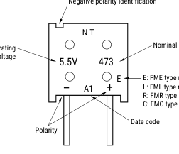
Nominal capacitance
Maximum operating
E: FME type marking L: FML type marking R: FMR type marking C: FMC type marking
Page 9
Packaging Quantities
| Part Number | Bulk Quantity per Box Straight Lead | Bulk Quantity per Box L1 Lead Option | Ammo Pack Quantity |
|---|---|---|---|
| FM0H103ZF | 1,000 pieces | 1,000 pieces | 1,000 pieces |
| FM0H223ZF | 1,000 pieces | 1,000 pieces | 1,000 pieces |
| FM0H473ZF | 1,000 pieces | 1,000 pieces | 1,000 pieces |
| FM0H104ZF | 1,000 pieces | 800 pieces | 1,000 pieces |
| FM0H224ZF | 1,000 pieces | 800 pieces | 1,000 pieces |
| FM0V473ZF | 1,000 pieces | 1,000 pieces | 1,000 pieces |
| FM0V104ZF | 1,000 pieces | 1,000 pieces | 1,000 pieces |
| FM0V224ZF | 1,000 pieces | 1,000 pieces | 1,000 pieces |
| FM0J473ZF | 1,000 pieces | 1,000 pieces | 1,000 pieces |
| FME0H223ZF | 1,000 pieces | 1,000 pieces | 1,000 pieces |
| FME0H473ZF | 1,000 pieces | 1,000 pieces | 1,000 pieces |
| FML0H333ZF | 1,000 pieces | 1,000 pieces | 1,000 pieces |
| FMR0H473ZF | 1,000 pieces | 1,000 pieces | 1,000 pieces |
| FMR0H104ZF | 1,000 pieces | 1,000 pieces | 1,000 pieces |
| FMR0V104ZF | 1,000 pieces | 1,000 pieces | 1,000 pieces |
| FMC0H473ZF | 1,000 pieces | 1,000 pieces | 1,000 pieces |
| FMC0H104ZF | 1,000 pieces | 1,000 pieces | 1,000 pieces |
| FMC0H334ZF | 400 pieces | 300 pieces | 400 pieces |
Page 10
Ammo Pack Taping Format (Except FMC0H334ZFTP)
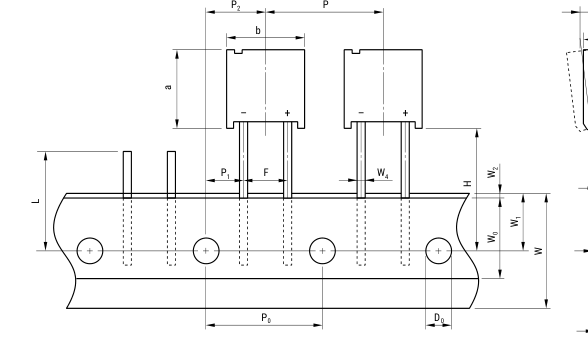
∆h
c
t3
t2
t1
Ammo Pack Taping Specifications (Except FMC0H334ZFTP)
| Item | Symbol | Dimensions (mm) |
|---|---|---|
| Component Height | a | 11.5±0.5 |
| Component Width | b | 10.5±0.5 |
| Component Thickness | c | Refer to “Dimensions” table |
| Lead-Wire Width | W 4 | 0.5±0.1 |
| Lead-Wire Thickness | t 3 | 0.4±0.1 |
| Component Pitch | P | 12.7±1.0 |
| Sprocket Hole Pitch | P 0 | 12.7±0.3 |
| Sprocket Hole Center to Lead Center | P 1 | 3.85±0.7 |
| Sprocket Hole Center to Component Center | P 2 | 6.35±0.7 |
| Lead Spacing | F | 5.0±0.5 |
| Component Alignment (side/side) | ∆h | 2.0 Maximum |
| Carrier Tape Width | W | 18.0+1.0/−0.5 |
| Hold-Down Tape Width | W 0 | 12.5 Minimum |
| Sprocket Hole Position | W 1 | 9.0±0.5 |
| Hold-Down Tape Position | W 2 | 3.0 Maximum |
| Height to Seating Plane (lead length) | H | 16.0±0.5/18.0±0.5 |
| Sprocket Hole Diameter | D 0 | ø 4.0±0.2 |
| Carrier Tape Thickness | t 1 | 0.7±0.2 |
| Total Thickness (Carrier Tape, Hold-Down Tape and Lead) | t 2 | 1.5 Maximum |
| Cut Out Length | L | 11.0 Maximum |
Page 11
Ammo Pack Taping Format (FMC0H334ZFTP)
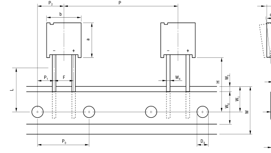
∆h
c
t3
t2
t1
Ammo Pack Taping Specifications (FMC0H334ZFTP)
| Item | Symbol | Dimensions (mm) |
|---|---|---|
| Component Height | a | 15.0±0.5 |
| Component Width | b | 14.0±0.5 |
| Component Thickness | c | 9.0±0.5 |
| Lead-Wire Width | W 4 | 0.6±0.1 |
| Lead-Wire Thickness | t 3 | 0.6±0.1 |
| Component Pitch | P | 25.4±1.0 |
| Sprocket Hole Pitch | P 0 | 12.7±0.3 |
| Sprocket Hole Center to Lead Center | P 1 | 3.85±0.7 |
| Sprocket Hole Center to Component Center | P 2 | 6.35±0.7 |
| Lead Spacing | F | 5.0±0.5 |
| Component Alignment (side/side) | ∆h | 2.0 Maximum |
| Carrier Tape Width | W | 18.0+1.0/−0.5 |
| Hold-Down Tape Width | W 0 | 12.5 Minimum |
| Sprocket Hole Position | W 1 | 9.0±0.5 |
| Hold-Down Tape Position | W 2 | 3.0 Maximum |
| Height to Seating Plane (lead length) | H | 16.0±0.5/18.0±0.5 |
| Sprocket Hole Diameter | D 0 | ø 4.0±0.2 |
| Carrier Tape Thickness | t 1 | 0.67±0.2 |
| Total Thickness (Carrier Tape, Hold-Down Tape and Lead) | t 2 | 1.7 Maximum |
| Cut Out Length | L | 11.0 Maximum |
Page 12
List of Plating & Sleeve Type
By changing the solder plating from leaded solder to lead-free solder and the outer tube material of can-cased conventional supercapacitor from polyvinyl chloride to polyethylene terephthalate (PET), our supercapacitor is now even friendlier to the
environment.
a. Iron + copper base + lead-free solder plating (Sn-1Cu) b. SUS nickel base + copper base + reflow lead-free solder plating (100% Sn, reflow processed)
| Series | Part Number | Plating | Sleeve |
|---|---|---|---|
| FM | All FM Series | a | No tube used |
Recommended Pb-free solder :
Sn / 3.5Ag / 0.75Cu Sn / 3.0Ag / 0.5Cu Sn / 0.7Cu Sn / 2.5Ag / 1.0Bi / 0.5Cu
Page 13
Measurement Conditions
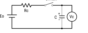
Capacitance (Charge System) Capacitance is calculated from expression (9) by measuring the charge time constant (τ) of the capacitor (C). Prior to
measurement, the capacitor is discharged by shorting both pins of the device for at least 30 minutes. In addition, use the polarity
indicator on the device to determine correct orientation of capacitor for charging.
Eo: 3.0 (V) Product with maximum operating voltage of 3.5 V
τ
Capacitance:
(F) (9)
C =
5.0 (V) Product with maximum operating voltage of 5.5 V
Rc
6.0 (V) Product with maximum operating voltage of 6.5 V
Switch
10.0 (V) Product with maximum operating voltage of 11 V
12.0 (V) Product with maximum operating voltage of 12 V
τ:
Time from start of charging until Vc becomes 0.632 Eo (V)
(seconds) Rc: See table below (Ω).
Charge Resistor Selection Guide
| Cap | FA | FE | FS | FY | FR | FM, FME FMR, FML | FMC | FG FGR | FGH | FT | FC, FCS | HV | ||
| FYD | FYH | FYL | ||||||||||||
| 0.010 F | – | – | – | – | – | 5000 Ω | – | 5000 Ω | – | 5000 Ω | – | – | – | – |
| 0.022 F | 1000 Ω | – | 1000 Ω | 2000 Ω | 2000 Ω | 2000 Ω | 2000 Ω | 2000 Ω | – | 2000 Ω | – | – | Discharge | – |
| 0.033 F | – | – | – | – | – | – | – | Discharge | – | – | – | – | – | – |
| 0.047 F | 1000 Ω | 1000 Ω | 1000 Ω | 2000 Ω | 1000 Ω | 2000 Ω | 1000 Ω | 2000 Ω | 1000 Ω | 2000 Ω | – | – | – | – |
| 0.10 F | 510 Ω | 510 Ω | 510 Ω | 1000 Ω | 510 Ω | – | 1000 Ω | 1000 Ω | 1000 Ω | 1000 Ω | Discharge | 510 Ω | Discharge | – |
| 0.22 F | 200 Ω | 200 Ω | 200 Ω | 510 Ω | 510 Ω | – | 510 Ω | 0H: Discharge 0V: 1000 Ω | – | 1000 Ω | Discharge | 200 Ω | Discharge | – |
| 0.33 F | – | – | – | – | – | – | – | – | Discharge | – | – | – | – | – |
| 0.47 F | 100 Ω | 100 Ω | 100 Ω | 200 Ω | 200 Ω | – | 200 Ω | – | – | 1000 Ω | Discharge | 100 Ω | Discharge | – |
| 1.0 F | 51 Ω | 51 Ω | 100 Ω | 100 Ω | 100 Ω | – | 100 Ω | – | – | 510 Ω | Discharge | 100 Ω | Discharge | Discharge |
| 1.4 F | – | – | – | 200 Ω | – | – | – | – | – | – | – | – | – | – |
| 1.5 F | – | 51 Ω | – | – | – | – | – | – | – | 510 Ω | – | – | – | – |
| 2.2 F | – | – | – | 100 Ω | – | – | – | – | – | 200 Ω | – | 51 Ω | – | – |
| 2.7 F | – | – | – | – | – | – | – | – | – | – | – | – | – | Discharge |
| 3.3 F | – | – | – | – | – | – | – | – | – | – | – | 51 Ω | – | – |
| 4.7 F | – | – | – | – | – | – | – | – | – | 100 Ω | – | – | – | Discharge |
| 5.0 F | – | – | 100 Ω | – | – | – | – | – | – | – | – | – | – | – |
| 5.6 F | – | – | – | – | – | – | – | – | – | – | – | 20 Ω | – | – |
| 10.0 F | – | – | – | – | – | – | – | – | – | – | – | – | – | Discharge |
| 22.0 F | – | – | – | – | – | – | – | – | – | – | – | – | – | Discharge |
| 50.0 F | – | – | – | – | – | – | – | – | – | – | – | – | – | Discharge |
| 100.0 F | – | – | – | – | – | – | – | – | – | – | – | – | – | Discharge |
| 200.0 F | – | – | – | – | – | – | – | – | – | – | – | – | – | Discharge |
\*Capacitance values according to the constant current discharge method. \*HV Series capacitance is measured by discharge system
Page 14
51 Ω
3.3F – – – – – – – – – – –
–
100 Ω
4.7F – – – – – – – – –
– – –
100 Ω
5.0F – –
– – – – – – – – – – 20 Ω
5.6F – – – – – – – – – – –
–
\*Capacitance values according to the constant current discharge method. \*HV series capacitance is measured by discharge system.
Table 3 Capacitance measurement
Measurement Conditions cont’d
Capacitance (Discharge System)
Capacitance (Discharge System)
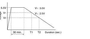
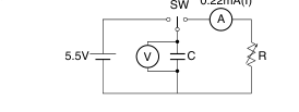
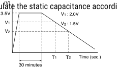
In the diagram below, charging is performed for a duration of 30 minutes, once the voltage of the condensor terminal
Capacitance (Discharge System:3.5V)
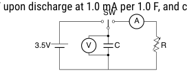
As shown in the diagram below, charging is performed for a duration of 30 minutes once the voltage of the capacitor
reaches 5.5 V. In the diagram below, charging is performed for a duration of 30 minutes, once the voltage of the capacitor terminal reaches 3.5V.
terminal reaches 5.5 V. Then, use a constant current load device and measure the time for the terminal voltage to drop
Then, use a constant current load device and measure the time for the terminal voltage to drop from 3.0 to 2.5 V upon Then, use a constant current load device and measure the time for the terminal voltage to drop from 1.8 to 1.5V upon
from 3.0 to 2.5 V upon discharge at 0.22 mA per 0.22 F, for example, and calculate the static capacitance according to the discharge at 0.22 mA for 0.22 F, for example, and calculate the static capacitance according to the equation shown below. discharge at 1 mA per 1F, and calculate the static capacitance according to the equation shown below.
equation shown below.
Note: The current value is 1 mA discharged per 1F.
(V)
Note: The current value is 1 mA discharged per 1 F.
0.22mA(I)
I×(T2-T1) I×(T2-T1)
C= (F) Capactance:C= (F) V1-V2 V1-V2
30 minutes
Capacitance (Discharge System:3.5V)
Capacitance (Discharge System:3.5V)
Capacitance (Discharge System:3.5V)
Capacitance (Discharge System:3.5V)
Capacitance (Discharge System:HVseries)
36 Super Capacitors Vol.13
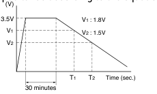
Capacitance (Discharge System – 3.5 V)
In the diagram below, charging is performed for a duration of 30 minutes, once the voltage of the capacitor terminal reaches In the diagram below, charging is performed for a duration of 30 minutes, once the voltage of the capacitor terminal reaches 3.5V. In the diagram below, charging is performed for a duration of 30 minutes, once the voltage of the capacitor terminal reaches In the diagram below, charging is performed for a duration of 30 minutes, once the voltage of the capacitor terminal reaches 3.5V.
As shown in the diagram below, charging is performed for a duration of 30 minutes once the voltage of the capacitor
In the diagram below, charging is performed for a duration of 30 minutes, once the voltage of the capacitor terminal reaches Then, use a constant current load device and measure the time for the terminal voltage to drop from 1.8 to 1.5V Then, use a constant current load device and measure the time for the terminal voltage to drop from 1.8 to 1.5V upon Then, use a constant current load device and measure the time for the terminal voltage to drop from 1.8 to 1.5V Then, use a constant current load device and measure the time for the terminal voltage to drop from 1.8 to 1.5V upon
terminal reaches 3.5 V. Then, use a constant current load device and measure the time for the terminal voltage to drop from
Max. operating voltage. discharge at 1 mA per 1F, and calculate the static capacitance according to the equation shown below. discharge at 1 mA per 1F, and calculate the static capacitance according to the equation shown below. discharge at 1 mA per 1F, and calculate the static capacitance according to the equation shown below. discharge at 1 mA per 1F, and calculate the static capacitance according to the equation shown below. Then, use a constant current load device and measure the time for the terminal voltage to drop from 2.0 to 1.5V upon discharge
1.8 to 1.5 V upon discharge at 1.0 mA per 1.0 F, for example, and calculate the static capacitance according to the equation
(V) (V)
at 1 mA per 1F, and calculate the static capacitance according to the equation shown below.
(V)
shown below.
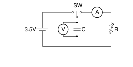
I×(T2-T1) I×(T2-T1) I×(T2-T1) I×(T2-T1) C= (F) C= (F) C= (F) C= (F)
V1-V2 V1-V2 V1-V2 V1-V2 I×(T2-T1) C= (F) V1-V2
Capacitance (Discharge System:HVseries)
T1 T2 Time (sec.)
Capacitance (Discharge System:HVseries)
Capacitance (Discharge System:HVseries)
Capacitance (Discharge System:HVseries)
30 minutes
In the diagram below, charging is performed for a duration of 30 minutes, once the voltage of the capacitor terminal re In the diagram below, charging is performed for a duration of 30 minutes, once the voltage of the capacitor terminal reaches In the diagram below, charging is performed for a duration of 30 minutes, once the voltage of the capacitor terminal re In the diagram below, charging is performed for a duration of 30 minutes, once the voltage of the capacitor terminal reaches
Equivalent series resistance (ESR)
Max. operating voltage. Max. operating voltage. Max. operating voltage.
Capacitance (Discharge System – HV Series)
Max. operating voltage. ESR shall be calculated from the equation below. Then, use a constant current load device and measure the time for the terminal voltage to drop from 2.0 to 1.5V upon disc Then, use a constant current load device and measure the time for the terminal voltage to drop from 2.0 to 1.5V upon discharge Then, use a constant current load device and measure the time for the terminal voltage to drop from 2.0 to 1.5V upon disc
As shown in the diagram below, charging is performed for a duration of 30 minutes once the voltage of the capacitor
Then, use a constant current load device and measure the time for the terminal voltage to drop from 2.0 to 1.5V upon discharge at 1 mA per 1F, and calculate the static capacitance according to the equation shown below. at 1 mA per 1F, and calculate the static capacitance according to the equation shown below. at 1 mA per 1F, and calculate the static capacitance according to the equation shown below. at 1 mA per 1F, and calculate the static capacitance according to the equation shown below.
terminal reaches maximum operating voltage. Then, use a constant current load device and measure the time for the
10mA
terminal voltage to drop from 2.0 to 1.5 V upon discharge at 1.0 mA per 1.0 F, and calculate the static capacitance according
VC
ESR= (Ω) 0.01
to the equation shown below.
I×(T2-T1) I×(T2-T1) I×(T2-T1) I×(T2-T1) C= (F) C= (F) C= (F) C= (F)
V1-V2 V1-V2 V1-V2 V1-V2
Current (at 30 minutes after charging)
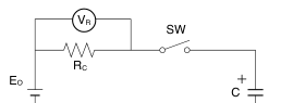
Current shall be calculated from the equation below. Prior to measurement, both lead terminals must be short-circuited for a minimum of 30 minutes.
30 minutes 30 minutes
Equivalent series resistance (ESR)
Equivalent series resistance (ESR)
The lead terminal connected to the metal can case is connected to the negative side of the power supply.
Equivalent series resistance (ESR)
Equivalent series resistance (ESR)
ESR shall be calculated from the equation below. ESR shall be calculated from the equation below. ESR shall be calculated from the equation below. ESR shall be calculated from the equation below. Eo: 2.5Vdc (HVseries 50F)
VR
2.7Vdc (HVseries except 50F)
SW
10mA 10mA 10mA
VC VC
10mA
3.0Vdc (3.5V type)
VC ESR= (Ω) ESR= (Ω) VC ESR= (Ω) ESR= (Ω)
f:1kHz
C
VC
f:1kHz
C
VC
0.01
f:1kHz
C
VC RC
0.01 5.0Vdc (5.5V type)
f:1kHz
C
VC
0.01
+
0.01
EO
Rc: 1000Ω (0.010F, 0.022F, 0.047F)
C -
100Ω (0.10F, 0.22F, 0.47F) 10Ω (1.0F, 1.5F, 2.2F, 4.7F)
Current (at 30 minutes after charging)
Current (at 30 minutes after charging)
Current (at 30 minutes after charging)
Current (at 30 minutes after charging)
2.2Ω (HVseries) Current shall be calculated from the equation below. Current shall be calculated from the equation below. Current shall be calculated from the equation below. VR
Current shall be calculated from the equation below. Current= (A) Prior to measurement, both lead terminals must be short-circuited for a minimum of 30 minutes. Prior to measurement, both lead terminals must be short-circuited for a minimum of 30 minutes. Prior to measurement, both lead terminals must be short-circuited for a minimum of 30 minutes. Prior to measurement, both lead terminals must be short-circuited for a minimum of 30 minutes.
RC The lead terminal connected to the metal can case is connected to the negative side of the power supply. The lead terminal connected to the metal can case is connected to the negative side of the power supply. The lead terminal connected to the metal can case is connected to the negative side of the power supply. The lead terminal connected to the metal can case is connected to the negative side of the power supply.
Self-discharge characteristic (0H: 5.5V products)
Eo: 2.5Vdc (HVseries 50F) Eo: 2.5Vdc (HVseries 50F) Eo: 2.5Vdc (HVseries 50F) Eo: 2.5Vdc (HVseries 50F) The self-discharge characteristic is measured by charging a voltage of 5 0 Vdc (charge protection resistance: 0Ω) according
VR VR
2 7Vdc (HVse ies e cept 50F) 2 7Vd (HV i
t 50F)
V
Page 15
at 1 mA per 1F, and calculate the static capacitance according to the equation shown below.
(V)
T1 T2

ESR= (Ω)
f:1kHz
C
VC
0.01
30 minutes
Equivalent series resistance (ESR)
Equivalent Series Resistance (ESR)
Equivalent series resistance (ESR)
ESR shall be calculated from the equation below.
ESR shall be calculated from the equation below.
ESR shall be calculated from the equation below.
Current (at 30 minutes after charging)
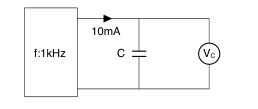
VC ESR= (Ω) VC 0.01 Prior to measurement, both lead terminals must be short-circuited for a minimum of 30 minute
ESR= (Ω) 0.01 The lead terminal connected to the metal can case is connected to the negative side of the po
Current (at 30 minutes after charging)
Current (at 30 minutes after charging)
VR
2.7Vdc (HVseries except 50F)
Current (at 30 minutes after charging)
SW
Current shall be calculated from the equation below.
Current shall be calculated from the equation below. Prior to measurement, both lead terminals must be short-circuited for
3.0Vdc (3.5V type)
Prior to measurement, both lead terminals must be short-circuited for a minimum of 30 minutes. Current shall be calculated from the equation below.
a minimum of 30 minutes. The lead terminal connected to the metal can case is connected to the negative side of the power
RC
5.0Vdc (5.5V type)
The lead terminal connected to the metal can case is connected to the negative side of the power supply. Prior to measurement, both lead terminals must be short-circuited for a minimum of 30 minutes.
+
EO
Rc: 1000Ω (0.010F, 0.022F, 0.047F)
supply.
C
The lead terminal connected to the metal can case is connected to the negative side of the power supply.
-
100Ω (0.10F, 0.22F, 0.47F)
Eo: 2.5Vdc (HVseries 50F)
10Ω (1.0F, 1.5F, 2.2F, 4.7F)
Eo: 2.5 VDC (HV Series 50 F)
Eo: 2.5Vdc (HVseries 50F) 2.7Vdc (HVseries except 50F)
2.2Ω (HVseries)
2.7 VDC (HV Series except 50 F)
3.0Vdc (3.5V type) 2.7Vdc (HVseries except 50F)
3.0 VDC (3.5 V type)
VR
Current= (A) 5.0Vdc (5.5V type) 3.0Vdc (3.5V type)
5.0 VDC (5.5 V type)
Rc: 1000Ω (0.010F, 0.022F, 0.047F)
RC
Rc: 1000 Ω (0.010 F, 0.022 F, 0.047 F)
5.0Vdc (5.5V type)
+ -
EO
100 Ω (0.10 F, 0.22 F, 0.47 F) 100Ω (0.10F, 0.22F, 0.47F)
Rc: 1000Ω (0.010F, 0.022F, 0.047F)
C
Self-discharge characteristic (0H: 5.5V products)
-
10 Ω (1.0 F, 1.5 F, 2.2 F, 4.7 F)
10Ω (1.0F, 1.5F, 2.2F, 4.7F) 100Ω (0.10F, 0.22F, 0.47F)
2.2 Ω (HV Series)
2.2Ω (HVseries) 10Ω (1.0F, 1.5F, 2.2F, 4.7F)
The self-discharge characteristic is measured by charging a voltage of 5.0 Vdc (charge protec
2.2Ω (HVseries)
to the capacitor polarity for 24 hours, then releasing between the pins for 24 hours and measu VR
Current= (A)
Self-Discharge Characteristic (0H – 5.5 V Products)
The test should be carried out in an environment with an ambient temperature of 25℃ or belo VR RC
Current= (A)
The self-discharge characteristic is measured by charging a voltage of 5.0 VDC (charge protection resistance: 0 Ω)
RH or below. RC
according to the capacitor polarity for 24 hours, then releasing between the pins for 24 hours and measuring the pin-to-
Self-discharge characteristic (0H: 5.5V products)
pin voltage. The test should be carried out in an environment with an ambient temperature of 25° C or below and relative
Su
Self-discharge characteristic (0H: 5.5V products)
The self-discharge characteristic is measured by charging a voltage of 5.0 Vdc (charge protection resistance
humidity of 70% RH or below.
The self-discharge characteristic is measured by charging a voltage of 5.0 Vdc (charge protection resistance: 0Ω) to the capacitor polarity for 24 hours, then releasing between the pins for 24 hours and measuring the pin-to-
the soldering is checked.
The test should be carried out in an environment with an ambient temperature of 25℃ or below and relative to the capacitor polarity for 24 hours, then releasing between the pins for 24 hours and measuring the pin-to-pin vo The test should be carried out in an environment with an ambient temperature of 25℃ or below and relative humid RH or below.
4. Dismantling
RH or below.
There is a small amount of electrolyte stored within the capacitor. Do not attempt to dismantle as direct skin contact with
Super Capacito
the electrolyte will cause burning. This product should be treated as industrial waste and not is not to be disposed of by fire.
Super Capacitors V
Page 16
Notes on Using Supercapacitors or Electric Double-Layer Capacitors (EDLCs)
- Circuitry Design 1.1 Useful life The FC Series Supercapacitor (EDLC) uses an electrolyte in a sealed container. Water in the electrolyte can evaporate while in use over long periods of time at high temperatures, thus reducing electrostatic capacity which in turn will create greater internal resistance. The characteristics of the supercapacitor can vary greatly depending on the environment in which it is used. Basic breakdown mode is an open mode due to increased internal resistance.
1.2 Fail rate in the field Based on field data, the fail rate is calculated at approximately 0.006 Fit. We estimate that unreported failures are ten times this amount. Therefore, we assume that the fail rate is below 0.06 Fit.
1.3 Exceeding maximum usable voltage Performance may be compromised and in some cases leakage or damage may occur if applied voltage exceeds maximum working voltage.
1.4 Use of capacitor as a smoothing capacitor (ripple absorption) As supercapacitors contain a high level of internal resistance, they are not recommended for use as smoothing capacitors in electrical circuits. Performance may be compromised and, in some cases, leakage or damage may occur if a supercapacitor is used in ripple absorption.
1.5 Series connections As applied voltage balance to each supercapacitor is lost when used in series connection, excess voltage may be applied to some supercapacitors, which will not only negatively affect its performance but may also cause leakage and/or damage. Allow ample margin for maximum voltage or attach a circuit for applying equal voltage to each supercapacitor (partial pressure resistor/voltage divider) when using supercapacitors in series connection. Also, arrange supercapacitors so that the temperature between each capacitor will not vary.
1.6 Case Polarity The supercapacitor is manufactured so that the terminal on the outer case is negative (-). Align the (-) symbol during use. Even though discharging has been carried out prior to shipping, any residual electrical charge may negatively affect other parts.
1.7 Use next to heat emitters Useful life of the supercapacitor will be significantly affected if used near heat emitting items (coils, power transistors and posistors, etc.) where the supercapacitor itself may become heated.
1.8 Usage environment This device cannot be used in any acidic, alkaline or similar type of environment.
Page 17
Notes on Using Supercapacitors or Electric Double-Layer Capacitors (EDLCs) cont’d
- Mounting 2.1 Mounting onto a reflow furnace Except for the FC series, it is not possible to mount this capacitor onto an IR / VPS reflow furnace. Do not immerse the capacitor into a soldering dip tank.
2.2 Flow soldering conditions See Recommended Reflow Curves in Section – Precautions for Use
2.3 Installation using a soldering iron Care must be taken to prevent the soldering iron from touching other parts when soldering. Keep the tip of the soldering iron under 400ºC and soldering time to within 3 seconds. Always make sure that the temperature of the tip is controlled. Internal capacitor resistance is likely to increase if the terminals are overheated.
2.4 Lead terminal processing Do not attempt to bend or polish the capacitor terminals with sand paper, etc. Soldering may not be possible if the metallic plating is removed from the top of the terminals.
2.5 Cleaning, Coating, and Potting Except for the FM series, cleaning, coating and potting must not be carried out. Consult KEMET if this type of procedure is necessary. Terminals should be dried at less than the maximum operating temperature after cleaning.
- Storage 3.1 Temperature and humidity Make sure that the supercapacitor is stored according to the following conditions: Temperature: 5 – 35ºC (Standard 25ºC), Humidity: 20 – 70% (Standard: 50%). Do not allow the build up of condensation through sudden temperature change.
3.2 Environment conditions Make sure there are no corrosive gasses such as sulfur dioxide, as penetration of the lead terminals is possible. Always store this item in an area with low dust and dirt levels. Make sure that the packaging will not be deformed through heavy loading, movement and/or knocks. Keep out of direct sunlight and away from radiation, static electricity and magnetic fields.
3.3 Maximum storage period This item may be stored up to one year from the date of delivery if stored at the conditions stated above.
Page 18
KEMET Electronic Corporation Sales Offi ces
For a complete list of our global sales offi ces, please visit www.kemet.com/sales.
Disclaimer
This product has been made available through a Private Label Agreement and a Development and Cross-Licensing Agreement between KEMET and NEC TOKIN to expand market and product offerings for both companies and their respective customers. For more information, please visit http://www.kemet.com/nectokin. All product specifi cations, statements, information and data (collectively, the “Information”) in this datasheet are subject to change. The customer is responsible for checking and verifying the extent to which the Information contained in this publication is applicable to an order at the time the order is placed. All Information given herein is believed to be accurate and reliable, but it is presented without guarantee, warranty, or responsibility of any kind, expressed or implied.
Statements of suitability for certain applications are based on KEMET Electronics Corporation’s (“KEMET”) knowledge of typical operating conditions for such applications, but are not intended to constitute – and KEMET specifi cally disclaims – any warranty concerning suitability for a specifi c customer application or use. The Information is intended for use only by customers who have the requisite experience and capability to determine the correct products for their application. Any technical advice inferred from this Information or otherwise provided by KEMET with reference to the use of KEMET’s products is given gratis, and KEMET assumes no obligation or liability for the advice given or results obtained.
Although KEMET designs and manufactures its products to the most stringent quality and safety standards, given the current state of the art, isolated component failures may still occur. Accordingly, customer applications which require a high degree of reliability or safety should employ suitable designs or other safeguards (such as installation of protective circuitry or redundancies) in order to ensure that the failure of an electrical component does not result in a risk of personal injury or property damage. Although all product–related warnings, cautions and notes must be observed, the customer should not assume that all safety measures are indicted or that other
measures may not be required.
KEMET is a registered trademark of KEMET Electronics Corporation.