

 Download PDF
DATASHEET SEARCH SITE
Document overview
- PDF pages: 20
Technical content
Page 1
Features
- Complete AC-DC PCB-mounted solution
- Active Power Factor Correction (PFC)
- Rectification
- Filtering
- Transient protection
- Low profile package, 9.55mm height above board
- Power density: 121 W/in3, 330 W in 7.2 in2 footprint
- Consistent high efficiency over world-wide AC mains (85 – 264 Vac)
- Secondary-side energy storage
- SELV 48 V Output – Efficient power distribution to POL converters
- 3,000 Vac /4,242 Vdc isolation
- PFC (THD) exceeds EN61000-3-2 requirements
- Conducted emissions EN55022, Class B (with a few external components)
- Surge immunity EN61000-4-5
- ZVS high frequency (MHz) switching
- Low profile, high-density filtering
- 100 °C baseplate operation
Nomenclature
® US C
C NRTL US
Complete AC-DC PCB-mounted solution
Typical Applications
- LED - Lighting, display, signage
- Telecom (WiMAX, Power Amplifiers, Optical Switches)
- Automatic Test Equipment (ATE)
- High Efficiency Server Power
- Office Equipment (Printers, Copiers, Projectors)
- Industrial Equipment (Process Controllers, Material Handling, Factory Automation)
Product Overview
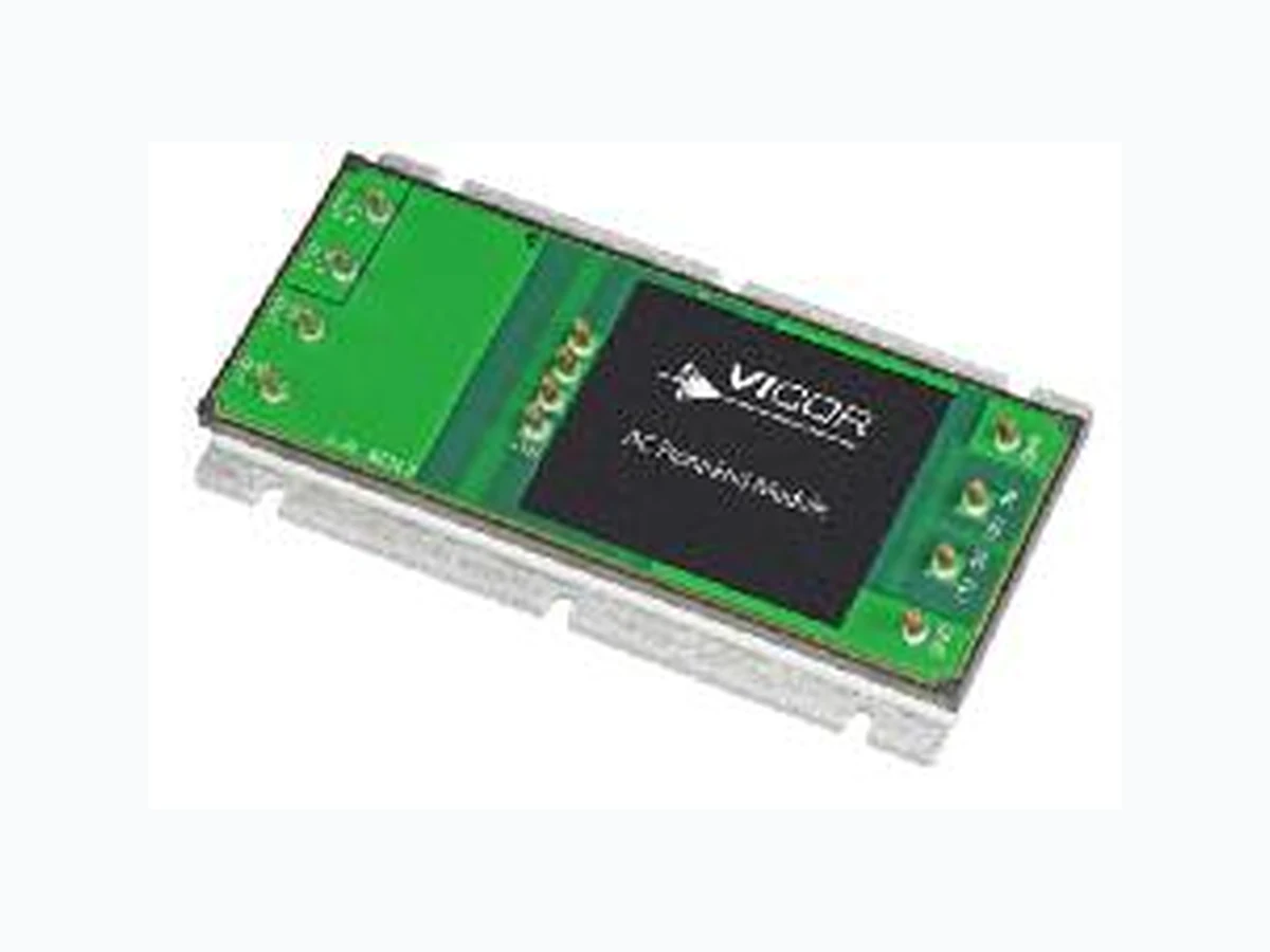
The VI BRICK® AC Front End is an AC-to-DC converter, operating from a universal AC input to generate an isolated and regulated 48 Vdc output with power factor correction. The module incorporates rectification, transient and surge suppression and AC to DC conversion to provide a complete AC to DC solution in a thin profile package. With its ZVS high frequency Adaptive CellTM topology, the VI BRICK AC Front End module consistently delivers high efficiency across worldwide AC mains. Downstream DC-DC converters support secondaryside energy storage and efficient power distribution, providing superior power system performance and connectivity from the wall plug to the point-of-load.
Major Specifications

| Function | Input Voltage Designator | Package Size | Output Voltage Vout (V) (x10) | Temperature Grade | Output Power Pout (W) (–:10) | Baseplate | Pin Style | Revision | |||||||||
| F | E | 1 | 7 | 5 | D | 4 | 8 | 0 | C | 0 | 3 | 3 | F | P | – | 0 | 0 |
| Universal (85 – 264 Vac) Grade Operating Storage F = Slotted Flange C = -20 to 100 °C -40 to 125 °C T = -40 to 100 °C -40 to 125 °C P = Through hole M = -55 to 100 °C -65 to 125 °C | |||||||||||||||||
Page 1 of 20
Page 2
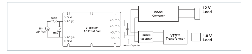
Typical Application: Universal AC to 12 V and 1 V, total 300 W
Absolute Maximum Ratings
The ABSOLUTE MAXIMUM Ratings below are stress ratings only. Operation at or beyond these maximum ratings can cause permanent damage to device. Electrical specifications do not apply when operating beyond rated operating conditions. Positive pin current represents current flowing out of the pin.
| Parameter Input voltage AC (L) to AC (N) Input voltage AC (L) to AC (N) Input voltage slew rate RSV1 to –IN EN to –IN RSV3 to –IN Output voltage (+Out to -Out) Output current Temperature Operating junction Operating temperature Storage temperature Dielectric Withstand Dielectric Withstand Input – Output Dielectric Withstand Input – Base Dielectric Withstand Output – Base | Comments | Min | Max | Unit V AC Vpk V/µs V DC V DC V DC V DC A °C °C °C °C °C °C °C V RMS V RMS V RMS |
| Continuous | 275 | |||
| 1 ms | 0 | 600 | ||
| 25 | ||||
| Do not connect to this pin | -0.3 | 5.3 | ||
| 5 V tolerant 3.3 V logic | -0.3 | 5.3 | ||
| Do not connect to this pin | -0.3 | 5.3 | ||
| -0.5 | 57.0 | |||
| 0.0 | 10.2 | |||
| Worst case semiconductor | 0 | 125 | ||
| C-Grade; baseplate | -20 | 100 | ||
| T-Grade; baseplate | -40 | 100 | ||
| M-Grade; baseplate | -55 | 100 | ||
| C-Grade | -40 | 125 | ||
| T-Grade | -40 | 125 | ||
| M-Grade | -65 | 125 | ||
| 3000 | ||||
| 1500 | ||||
| 1500 |
Page 2 of 20
Page 3
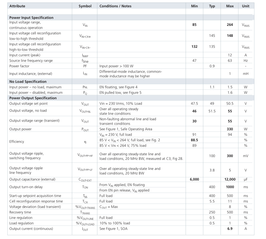
Electrical Characteristics
Specifications apply over all line and load conditions, 50 Hz and 60 Hz line frequencies, TC = 25 °C, unless otherwise noted. Boldface specifications apply over the temperature range of the specified Product Grade. COUT is 6800uF +/- 20% unless otherwise specified.
Page 3 of 20
Page 4
Electrical Characteristics (cont.)
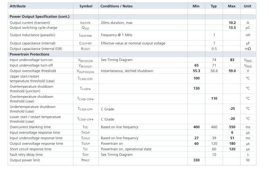
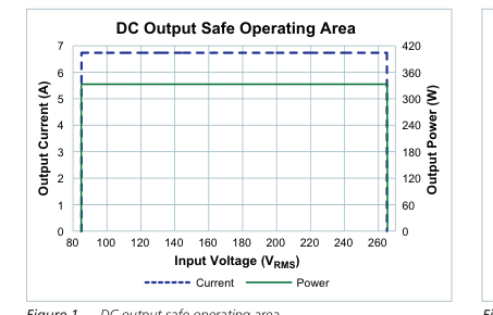
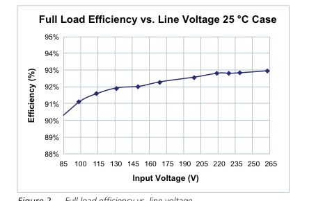
Figure 1 — DC output safe operating area
Figure 2 — Full load efficiency vs. line voltage
Page 4 of 20
Page 5
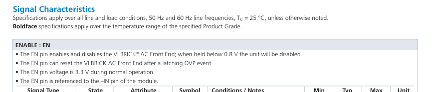
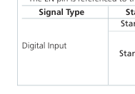
| State | Attribute | Symbol | Conditions / Notes | Min | Typ | Max |
|---|---|---|---|---|---|---|
| Startup | EN enable threshold | V EN_EN | 2.00 | |||
| Standby | EN disable time | T EN_DIS | From any point in line cycle | 9 | 16 | |
| EN disable threshold | V EN_DIS | 0.80 | ||||
| EN resistance to disable | R EN_EXT | Max allowable resistance to -IN required to disable the module | 14 |
V ms V kΩ
RESERVED : RSV1, RSV3
No connections should be made to these pins

Page 5 of 20
Page 6
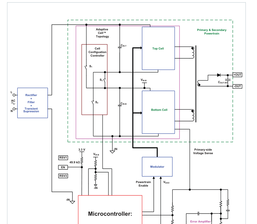
Functional Block Diagram




Page 6 of 20
Page 7
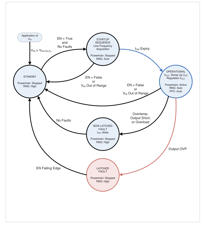
High Level Functional State Diagram
Conditions that cause state transitions are shown along arrows. Sub-sequence activities listed inside the state bubbles.
Page 7 of 20
Page 8
Timing Diagrams
Module Inputs are shown in blue; Module Outputs are shown in brown.
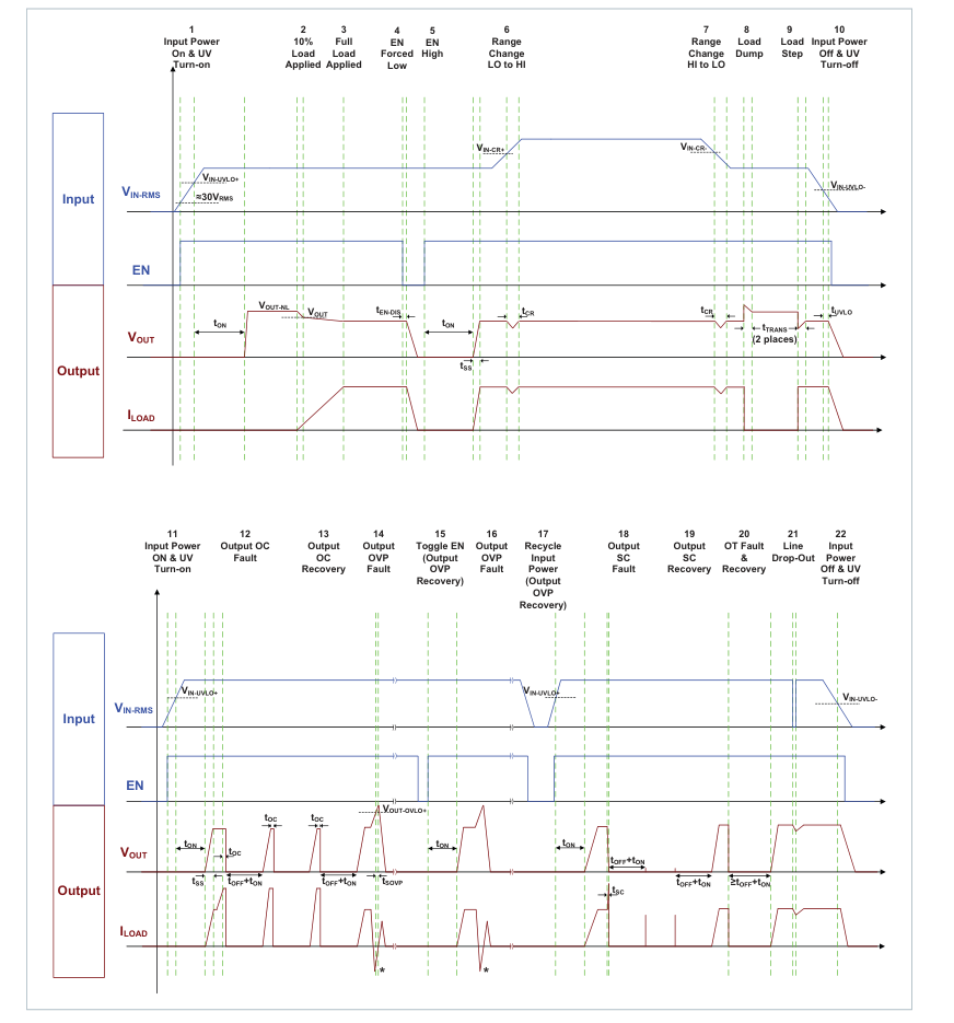
Figure 3 — Timing diagram - \* Negative current is externally forced and shown for the purpose of OVP protection scenario.
Page 8 of 20
Page 9
Application Characteristics
The following figures present typical performance at TC = 25 ºC, unless otherwise noted. See associated figures for general trend data.
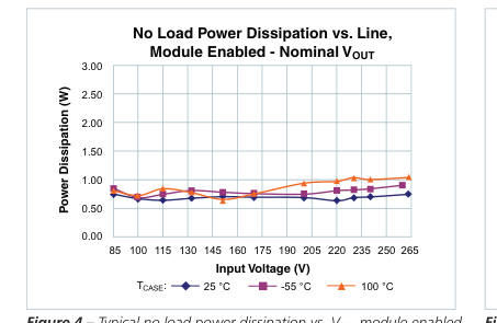
Figure 4 – Typical no load power dissipation vs. VIN, module enabled.
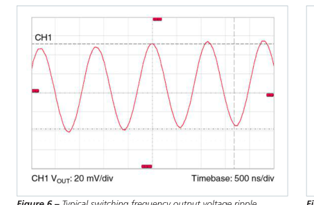
Figure 6 – Typical switching frequency output voltage ripple waveform, TCASE = 30 ºC, VIN = 230 V, IOUT = 6.9 A, no external ceramic capacitance.
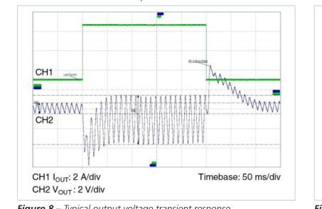
Figure 8 – Typical output voltage transient response, TCASE = 30 ºC, VIN = 230 V, IOUT = 6.9 A, COUT = 6,800 µF.
Page 9 of 20
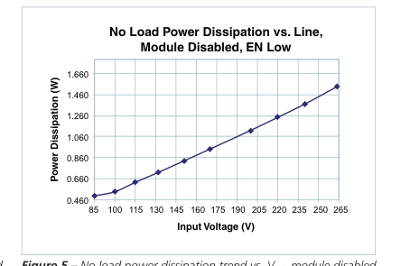
Figure 5 – No load power dissipation trend vs. VIN, module disabled.
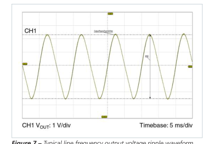
Figure 7 – Typical line frequency output voltage ripple waveform, TCASE = 30 ºC, VIN = 230 V, IOUT = 6.9 A, COUT = 6,800 µF. Measured at C3, Fig. 28.
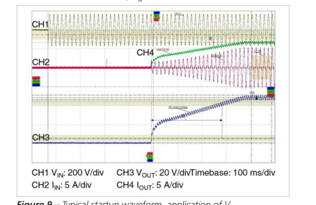
Figure 9 – Typical startup waveform, application of VIN, RLOAD = 7.1 Ω, COUT = 6,800 µF.
Page 10
Application Characteristics (cont.)
The following figures present typical performance at TC = 25 ºC, unless otherwise noted. See associated figures for general trend data.
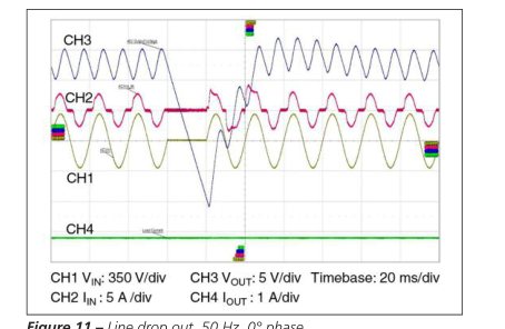
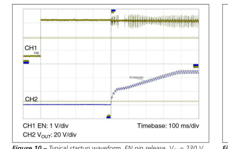
Figure 11 – Line drop out, 50 Hz, 0° phase,
Figure 10 – Typical startup waveform, EN pin release, VIN = 230 V, RLOAD = 7.1 Ω, COUT = 6,800 µF.
PLOAD = 330 W, COUT = 6,800 µF.
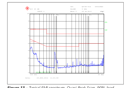
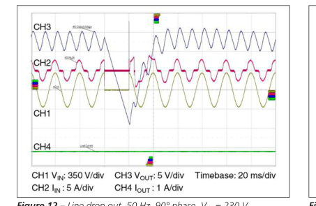
Figure 13 – Typical EMI spectrum, Quasi-Peak Scan, 90% load,
Figure 12 – Line drop out, 50 Hz, 90° phase, VIN = 230 V,
Output: 90% Load (297W)
230 VIN, COUT = 6,800 µF. Test circuit - Figure 28.
PLOAD = 330 W, COUT = 6,800 µF.
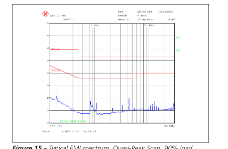
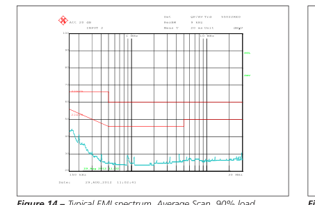
Figure 15 – Typical EMI spectrum, Quasi-Peak Scan, 90% load,
Figure 14 – Typical EMI spectrum, Average Scan, 90% load,
115 VIN, COUT = 6,800 µF. Test circuit - Figure 28.
230 VIN, COUT = 6,800 µF. Test circuit - Figure 28.
Page 10 of 20
Page 11
C
Application Characteristics (cont.)
O
The following figures present typical performance at TC = 25 ºC, unless otherwise noted. See associated figures for general trend data.
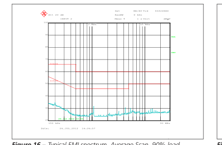
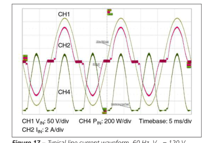
Figure 17 – Typical line current waveform, 60 Hz, VIN = 120 V,
Figure 16 – Typical EMI spectrum, Average Scan, 90% load,
PLOAD = 330 W. COUT = 6,800 µF.
115 VIN, COUT = 6,800 µF. Test circuit - Figure 28.
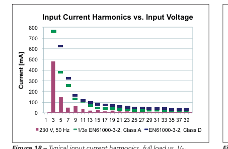
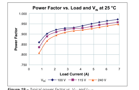
Figure 18 – Typical input current harmonics, full load vs. VIN.
Figure 19 – Typical power factor vs. VIN and IOUT.
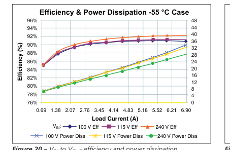
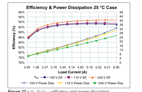
Figure 20 – VIN to VOUT efficiency and power dissipation
Figure 21 – VIN to VOUT efficiency and power dissipation
vs. VIN and IOUT, TCASE = -55 ºC.
vs. VIN and IOUT, TCASE = 25 ºC.
Page 11 of 20
Page 12
Application Characteristics (cont.)
The following figures present typical performance at TC = 25 ºC, unless otherwise noted. See associated figures for general trend data.
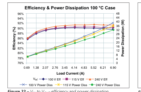
Figure 22 – VIN to VOUT efficiency and power dissipation
vs. VIN and IOUT, TCASE = 100 ºC.
Page 12 of 20
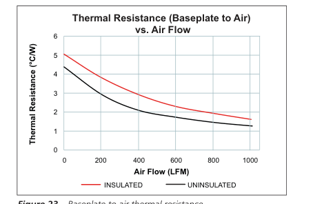
Figure 23 – Baseplate to air thermal resistance
Insulated – no thermal dissipation through pins to pcb; Uninsulated – thermal dissipation to typical pcb.
Page 13
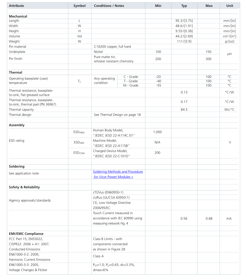
General Characteristics
Specifications apply over all line and load conditions, 50 Hz and 60 Hz line frequencies, TC = 25 °C, unless otherwise noted. Boldface specifications apply over the temperature range of the specified Product Grade.
Page 13 of 20
Page 14
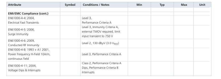
General Characteristics (cont.)
Specifications apply over all line and load conditions, 50 Hz and 60 Hz line frequencies, TC = 25 °C, unless otherwise noted. Boldface specifications apply over the temperature range of the specified Product Grade.
Product Outline Drawing and Recommended PCB Footprint
Module Outline
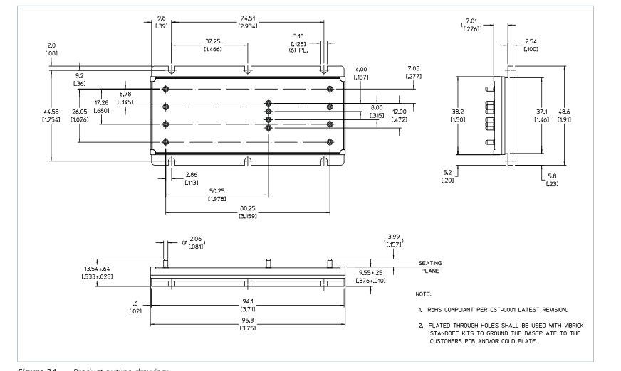
Figure 24 — Product outline drawing;
Product outline drawings are available in .pdf and .dxf formats. 3D mechanical models are available in .pdf and .step formats. See http://www.vicorpower.com/cms/home/technical_resources/Mechanical_Drawings/Modules for more details.
Page 14 of 20
Page 15
Product Outline Drawing and Recommended PCB Footprint (cont.)
Mounting Specifications
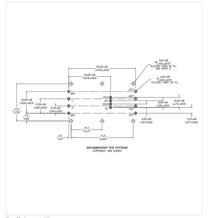
Figure 25— Recommended PCB pattern;
Product outline drawings are available in .pdf and .dxf formats. 3D mechanical models are available in .pdf and .step formats. See http://www.vicorpower.com/cms/home/technical_resources/Mechanical_Drawings/Modules for more details.
Page 15 of 20
Page 16
Product Details and Design Guidelines
Building Blocks and System Designs
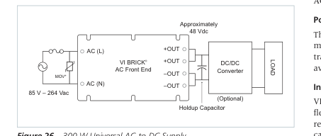
Figure 26 – 300 W Universal AC-to-DC Supply
The VI BRICK® AC Front End is a high efficiency AC-to-DC converter, operating from a universal AC input to generate an isolated SELV 48 VDC output bus with power factor correction. It is the key component of an AC-to-DC power supply system such as the one shown in Figure 26 above. The input to the VI BRICK AC Front End is a sinusoidal AC source with a power factor maintained by the module with harmonics conforming to IEC 61000-3-2. Internal filtering enables compliance with the standards relevant to the application (Surge, EMI, etc.). See EMI/EMC Compliance standards on page 13.
The module uses secondary-side energy storage (at the SELV 48 V bus) and optional PRM™ regulators to maintain output hold up through line dropouts and brownouts. Downstream regulators also provide tighter voltage regulation, if required. The FE175D480C033FP-00 is designed for standalone operation; however, it may be part of a system that is paralleled by downstream DC-DC converters. Contact Vicor Sales or refer to our website, www.vicorpower.com, regarding new models that can be paralleled
directly for higher power applications.
Traditional PFC Topology
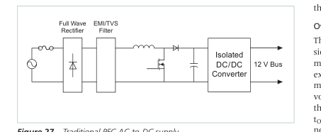
Figure 27 – Traditional PFC AC-to-DC supply
To cope with input voltages across worldwide AC mains (85 – 264 Vac), traditional AC-DC power supplies (Figure 27) use two power conversion stages: 1) a PFC boost stage to step up from a rectified input as low as 85 Vac to ~380 Vdc; and 2) a DC-DC down converter from 380 Vdc to a 12 V bus. The efficiency of the boost stage and of traditional power supplies is significantly compromised operating from worldwide AC lines as low as 85 Vac.
Adaptive Cell™ Topology With its single stage Adaptive Cell™ topology, the VI BRICK AC Front
Page 16 of 20
End enables consistently high efficiency conversion from worldwide AC mains to a 48 V bus and efficient secondary-side power distribution.
Power Factor Correction The module provides power factor correction over worldwide AC mains. For most static loads, PFC approaches unity, see Figure 19. Load transients that approach the line frequency should be filtered or avoided as these may reduce PFC.
Input Fuse Selection VI BRICK products are not internally fused in order to provide flexibility in configuring power systems. Input line fusing is recommended at system level, in order to provide thermal protection in case of catastrophic failure. The fuse shall be selected by closely matching system requirements with the following characteristics:
– Recommended fuse: 5 A, 216 Series Littelfuse – Current rating (usually greater than the VI BRICK AC Front End maximum current)
– Maximum voltage rating (usually greater than the maximum possible input voltage)
– Ambient temperature – Breaking capacity per application requirements – Nominal melting I2t
Fault Handling
Input Undervoltage (UV) Fault Protection The VI BRICK AC Front End’s input voltage (proportional to VIn-B as shown on page 6) is monitored by the micro-controller to detect an input under voltage condition. When the input voltage is less than the VIn-uVLo-, a fault is detected, the fault latch and reset logic disables the modulator, the modulator stops powertrain switching, and the output voltage of the unit falls. Aer a time tuVLo, the unit shuts down. Faults lasting less than tuVLo may not be detected. Such a fault does not go through an auto-restart cycle. once the input voltage rises above VInuVLo+, the unit recovers from the input uV fault, the powertrain
resumes normal switching aer a time ton and the output voltage of the unit reaches the set-point voltage within a time tSS.
Overcurrent (OC) Fault Protection The unit’s output current, determined by VEAo, VIn_B and the primaryside sensed output voltage, (as shown on page 6) is monitored by the microcontroller to detect an output oC condition. If the output current exceeds its current limit, a fault is detected, the reset logic disables the modulator, the modulator stops powertrain switching, and the output voltage of the module falls aer a time toC. As long as the fault persists, the module goes through an auto-restart cycle with off time equal to toFF + ton and on time equal to toC. Faults shorter than a time toC may not be detected. once the fault is cleared, the module follows its normal
start up sequence aer a time toFF.
Short Circuit (SC) Fault Protection The microcontroller determines a short circuit on the output of the unit by measuring its primary sensed output voltage and EAo (as shown on page 6). Most commonly, a drop in the primary-sensed output voltage triggers a short circuit event. The module responds to a short circuit event within a time tSC. The module then goes through an auto restart cycle, with an off time equal to toFF + ton and an on time equal to tSC, for as long as the short circuit fault condition persists. once the fault is cleared, the unit follows its normal start up sequence aer a time toFF. Faults shorter than a time tSC may not be detected.
Page 17
Product Details and Design Guidelines (cont.)
Temperature Fault Protection The microcontroller monitors the temperature within the VI BRICK AC Front End. If this temperature exceeds Tj-oTP+, an overtemperature fault is detected, the reset logic block disables the modulator, the modulator stops the powertrain switching and the output voltage of the VI BRICK AC Front End falls. once the case temperature falls below TCASE-oTP-, aer a time greater than or equal to toFF, the converter recovers and undergoes a normal restart. For the C- grade version of the converter, this temperature is 75 °C. Faults shorter than a time toTP may not be detected. If the temperature falls below TCASE-uTP-, an undertemperature fault is detected, the reset logic
disables the modulator, the modulator stops powertrain switching and the output voltage of the unit falls. once the case temperature rises above TCASE-uTP, aer a time greater than or equal to toFF, the unit recovers and undergoes a normal restart.
Output Overvoltage Protection (OVP) The microcontroller monitors the primary sensed output voltage (as shown on page 6) to detect output oVP. If the primary sensed output voltage exceeds VouT-oVLo+, a fault is latched, the logic disables the modulator, the modulator stops powertrain switching, and the output voltage of the module falls aer a time tSoVP. Faults shorter than a time tSoVP may not be detected. This type of fault is a latched fault and requires that 1) the En pin be toggled or 2) the input power be recycled to recover from the fault.
Hold-up Capacitance The VI BRICK AC Front End uses secondary-side energy storage (at the SELV 48 V bus) and optional PRM™ regulators to maintain output hold up through line dropouts and brownouts. The module’s output bulk capacitance can be sized to achieve the required hold up functionality.
Hold-up time depends upon the output power drawn from the VI BRICK AC Front End based AC-to-DC front end and the input voltage range of downstream DC-to-DC converters. The following formula can be used to calculate hold-up capacitance for a system comprised of VI BRICK AC Front End and a PRM™ regulator:
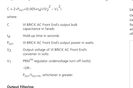
The VI BRICK AC Front End module requires an output bulk capacitor in the range of 6,000 µF to 12,000 µF for proper operation of the PFC front-end.
Page 17 of 20
The output voltage has the following two components of voltage ripple: 1) Line frequency voltage ripple: 2\*fLInE Hz component 2) Switching frequency voltage ripple: 1 MHz module switching frequency component
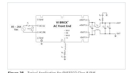
Figure 28 – Typical Application for EN55022 Class B EMI
Where, in the schematic: C1
2.2nF (Murata GA355DR7GF222KW01L)
C2
4.7nF (Murata GA355DR7GF472KW01L)
C3
3.3µF (TDK C4532X7R1H335MT)
C4
6800uF 63V (Panasonic UVR1J682MRD)
C5
100uF 63V (Nichicon UVY1J101MPD)
F1
5A, 216 Series Littlefuse
L1
15µH (TDK MLF2012C150KT)
L2
600µH (Vicor 37052-601)
MOV
300V, 10KA, 20mm dia (Littlefuse TMOV20RP300E) 6.8Ω
R1
2.2Ω
R2
Line Frequency Filtering output line frequency ripple depends upon output bulk capacitance. output bulk capacitor values should be calculated based on line frequency voltage ripple. High-grade electrolytic capacitors with adequate ripple current ratings, low ESR and a minimum voltage rating of 63 V are recommended.
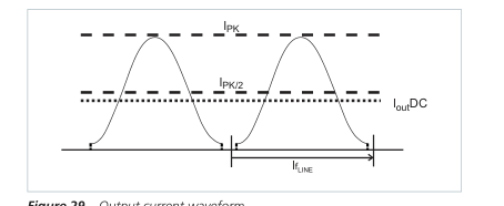
Figure 29 – Output current waveform
Page 18
Product Details and Design Guidelines (cont.)
Based on the output current waveform, as seen in Figure 29, the following formula can be used to determine peak-to-peak line frequency output voltage ripple:
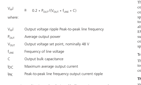
In certain applications, the choice of bulk capacitance may be determined by hold-up requirements and low frequency output voltage filtering requirements. Such applications may use the greater capacitance value determined from these requirements. The ripple current rating for the bulk capacitors can be determined from the following equation:
=~ Iripple
0.8 \* POUT / VOUT
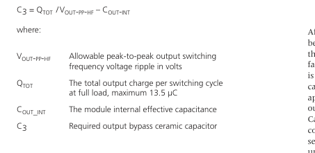
Switching Frequency Filtering Some applications require the output filtering shown in figure 28 to meet radiated emissions limits. In such a situation, the output switching ripple shown in figure 6 should be expected at the output of the filter. In cases where other means are used to control radiated emissions, and more ripple can be tolerated, the output filter can be simplified by removal of the common mode inductor, and C5, which is used to reduce the Q of the LC resonant tank. output switching frequency voltage ripple is the function of the output bypass ceramic capacitor. output bypass ceramic capacitor values should be calculated based on switching frequency voltage ripple.
normally bypass capacitors with low ESR are used with a sufficient voltage rating. output bypass ceramic capacitor value for allowable peak-to-peak switching frequency voltage ripple can be determined by:
Page 18 of 20
EMI Filtering and Transient Voltage Suppression
EMI Filtering The VI BRICK AC Front End with PFC is designed such that it will comply with En55022 Class B for Conducted Emissions with the filter connected across -In and GnD as shown in Figure 28. The emissions spectrum is shown in Figures 13-16. If one of the outputs is connected to earth ground, a small (single turn) output common mode choke is also required. EMI performance is subject to a wide variety of external influences such as PCB construction, circuit layout etc. As such, external components in addition to those listed herein may be required in specific instances to gain full compliance to the standards specified.
Transient Voltage Suppression The VI Brick AC Front End contains line transient suppression circuitry to meet specifications for surge (i.e. En61000-4-5) and fast transient conditions (i.e. En61000-4-4 fast transient/“burst”).
Thermal Design Thermal management of internally dissipated heat should maximize heat removed from the baseplate surface, since the baseplate represents the lowest aggregate thermal impedance to internal components. The baseplate temperature should be maintained below 100 °C. Cooling of the system PCB should be provided to keep the leads below 100 °C, and to control maximum PCB temperatures in the area of the module.
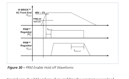
Powering a Constant Power Load When the output voltage of the VI BRICK AC Front End module is applied to the input of the PRM™ regulator, the regulator turns on and acts as a constant-power load. When the module’s output voltage reaches the input undervoltage turn on of the regulator, the regulator will attempt to start. However, the current demand of the PRM regulator at the undervoltage turn-on point and the hold-up capacitor charging current may force the VI BRICK AC Front End into current limit. In this case, the unit may shut down and restart repeatedly. In order to prevent this multiple restart scenario, it is necessary to delay enabling a constant-power load when powered up by the upstream AC
to 48 V front end until aer the output set point of the VI BRICK AC Front End is reached.
This can be achieved by 1) keeping the downstream constant-power load off during power up sequence and 2) turning the downstream constant-power load on aer the output voltage of the module reaches 48 V steady state.
Aer the initial startup, the output of the VI BRICK AC Front End can be allowed to fall to 30 V during a line dropout at full load. In this case, the circuit should not disable the PRM™ regulator if the input voltage falls aer it is turned on; therefore, some form of hysteresis or latching is needed on the enable signal for the constant power load. The output capacitance of the VI BRICK AC Front End should also be sized appropriately for a constant power load to prevent collapse of the output voltage of the module during line dropout (see Hold up Capacitance on page 17). A constant-power load can be turned off aer completion of the required hold up time during the power-down
sequence or can be allowed to turn off when it reaches its own undervoltage shutdown point.
Page 19
Product Details and Design Guidelines (cont.)
The timing diagram in Figure 30 shows the output voltage of the VI BRICK AC Front End module and the PRM PC pin voltage and output voltage of the PRM regulator for the power up and power down sequence. It is recommended to keep the time delay approximately 10 to 20 ms.
Special care should be taken when enabling the constant-power load near the auto-ranger threshold, especially with an inductive source upstream of the VI BRICK AC Front End. A load current spike may cause a large input voltage transient, resulting in a range change which could temporarily reduce the available power (see Adaptive Cell™ Topology below).
Adaptive Cell™ Topology The Adaptive Cell™ topology utilizes magnetically coupled “top” and “bottom” primary cells that are adaptively configured in series or parallel by a configuration controller comprised of an array of switches. A microcontroller monitors operating conditions and defines the configuration of the top and bottom cells through a range control signal.
A comparator inside the microcontroller monitors the line voltage and compares it to an internal voltage reference. If the input voltage of the VI BRICK AC Front End crosses above the positive going cell reconfiguration threshold voltage, the output of the comparator transitions, causing switches S1 and S2 to open and switch S3 to close (see Functional Block Diagram on page 6). With the top cell and bottom cell configured in series, the unit operates in “high” range and input capacitances CIn-T and CIn-B are in series.
If the peak of input voltage of the unit falls below the negative-going range threshold voltage for two line cycles, the cell configuration controller opens switch S3 and closes switches S1 and S2. With the top cell and bottom cells configured in parallel, the unit operates in “low” range and input capacitances CIn-T and CIn-B are in parallel.
Power processing is held off while transitioning between ranges and the output voltage of the unit may temporarily droop. External output hold up capacitance should be sized to support power delivery to the load during cell reconfiguration. The minimum specified external output capacitance of 6,000 µF is sufficient to provide adequate ridethrough during cell reconfiguration for typical applications.
Page 19 of 20
Page 20
Vicor’s comprehensive line of power solutions includes high density AC-DC and DC-DC modules and accessory components, fully configurable AC-DC and DC-DC power supplies, and complete custom power systems.
Information furnished by Vicor is believed to be accurate and reliable. However, no responsibility is assumed by Vicor for its use. Vicor makes no representations or warranties with respect to the accuracy or completeness of the contents of this publication. Vicor reserves the right to make changes to any products, specifications, and product descriptions at any time without notice. Information published by Vicor has been checked and is believed to be accurate at the time it was printed; however, Vicor assumes no responsibility for inaccuracies. Testing and other quality controls are used to the extent Vicor deems necessary to support Vicor’s product warranty. Except where mandated by government requirements, testing of all
parameters of each product is not necessarily performed. Specifications are subject to change without notice.
Vicor’s Standard Terms and Conditions
All sales are subject to Vicor’s Standard Terms and Conditions of Sale, which are available on Vicor’s webpage or upon request.
Product Warranty
In Vicor’s standard terms and conditions of sale, Vicor warrants that its products are free from non-conformity to its Standard Specifications (the “Express Limited Warranty”). This warranty is extended only to the original Buyer for the period expiring two (2) years after the date of shipment and is not transferable. UNLESS OTHERWISE EXPRESSLY STATED IN A WRITTEN SALES AGREEMENT SIGNED BY A DULY AUTHORIZED VICOR SIGNATORY, VICOR DISCLAIMS ALL REPRESENTATIONS, LIABILITIES, AND WARRANTIES OF ANY KIND (WHETHER ARISING BY IMPLICATION OR BY OPERATION OF LAW) WITH RESPECT TO THE PRODUCTS, INCLUDING, WITHOUT LIMITATION, ANY WARRANTIES OR REPRESENTATIONS AS TO MERCHANTABILITY, FITNESS FOR
PARTICULAR PURPOSE, INFRINGEMENT OF ANY PATENT, COPYRIGHT, OR OTHER INTELLECTUAL PROPERTY RIGHT, OR ANY OTHER MATTER.
This warranty does not extend to products subjected to misuse, accident, or improper application, maintenance, or storage. Vicor shall not be liable for collateral or consequential damage. Vicor disclaims any and all liability arising out of the application or use of any product or circuit and assumes no liability for applications assistance or buyer product design. Buyers are responsible for their products and applications using Vicor products and components. Prior to using or distributing any products that include Vicor components, buyers should provide adequate design, testing and operating safeguards. Vicor will repair or replace defective products in accordance with its own best judgment. For service under this warranty, the buyer must contact
Vicor to obtain a Return Material Authorization (RMA) number and shipping instructions. Products returned without prior authorization will be returned to the buyer. The buyer will pay all charges incurred in returning the product to the factory. Vicor will pay all reshipment charges if the product was defective within the terms of this warranty.
Life Support Policy
VICOR’S PRODUCTS ARE NOT AUTHORIZED FOR USE AS CRITICAL COMPONENTS IN LIFE SUPPORT DEVICES OR SYSTEMS WITHOUT THE EXPRESS PRIOR WRITTEN APPROVAL OF THE CHIEF EXECUTIVE OFFICER AND GENERAL COUNSEL OF VICOR CORPORATION. As used herein, life support devices or systems are devices which (a) are intended for surgical implant into the body, or (b) support or sustain life and whose failure to perform when properly used in accordance with instructions for use provided in the labeling can be reasonably expected to result in a significant injury to the user. A critical component is any component in a life support device or system whose failure to perform can be reasonably expected to cause the
failure of the life support device or system or to affect its safety or effectiveness. Per Vicor Terms and Conditions of Sale, the user of Vicor products and components in life support applications assumes all risks of such use and indemnifies Vicor against all liability and damages.
Intellectual Property Notice
Vicor and its subsidiaries own Intellectual Property (including issued U.S. and Foreign Patents and pending patent applications) relating to the products described in this data sheet. No license, whether express, implied, or arising by estoppel or otherwise, to any intellectual property rights is granted by this document. Interested parties should contact Vicor's Intellectual Property Department.
The products described on this data sheet are protected by the following U.S. Patents Numbers: 5,945,130; 6,403,009; 6,710,257; 6,911,848; 6,930,893; 6,934,166; 6,940,013; 6,969,909; 7,038,917; 7,166,898; 7,187,263; 7,361,844; D496,906; D505,114; D506,438; D509,472; and for use under 6,975,098 and 6,984,965.
Vicor Corporation 25 Frontage Road Andover, MA, USA 01810 Tel: 800-735-6200 Fax: 978-475-6715
Customer Service: custserv@vicorpower.com Technical Support: apps@vicorpower.com
Page 20 of 20