
CT110 ALLEGRO
Document overview
- Manufacturer or author: Provided By www.digicamel.com(free datasheet download site)
- PDF pages: 20
Technical content
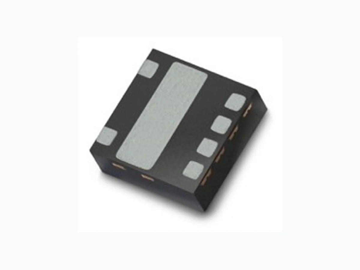
The CT110 is a high-linearity and high-resolution contact current sensor with isolation that is designed with its patented state-of- the-art XtremeSense™ TMR technology for high performance. The device measures the current flowing through the DFN package via its integrated current-carrying conductor (CCC) and converts it to an analog ratiometric output voltage that represents the current. The CT110 achieves superior performance with a typical total output error of less than ±0.5% and is capable of sensing current as low as 5 mA, providing unmatched resolution. The device supports a wide operating voltage range of 2.7 to 5.5 V which allows it to be used in a variety of applications. The CT110 is an ideal solution to replace a shunt resistor plus isolation amplifier. At the same time, the CT110 simplifies design, PCB layout, and saves PCB area. The device is capable of supporting up to 15.0 A of AC and DC current. The CT110 has a sampling frequency of 200 kHz but only has minimal current consumption of 1.0 mA to bias it since the measured current does not go through the device. Additionally, the CT110 integrates a FLAG output that is active low and will indicate when the field is above 90% and below 10% the full field range. The CT110 is available in a low-profile and small form factor 3.00 mm × 3.00 mm × 0.95 mm, 6-lead DFN package. CT110-DS, Rev. 3 MCO-0001515
- Current range: ±5.0 A, ±10.0 A, ±15.0 A
- Resolution: 5 mA
- Total output error: <±0.5% (Typical)
- 2 kV isolation per IEC 62368-1
- Sampling frequency: 200 kHz
- Supply current: ~1.2 mA
- FLAG pin to detect 90% and 10% of full current range □ Active low digital output (push-pull)
- Supply voltage: 2.7 to 5.5 V
- Operating temperature ranges: □ Industrial: –40°C to 85°C □ Extended Industrial: –40°C to 125°C
- Package: 6-lead DFN, 3.00 mm × 3.00 mm × 0.95 mm XtremeSense™ High-Linearity, High-Resolution TMR Current Sensor with FLAG Output in Miniature Form Factor PACKAGE: Not to scale CT110 FEATURES AND BENEFITS DESCRIPTION November 2, 2023
- Shunt resistor plus isolation amplifier replacement
- Smart plugs/IoT devices
- LED lighting products
- Power tools
- Appliances
- Drones
- Battery charger systems
- PCs and servers
APPLICATIONS
Figure 1: CT110 with Analog and FLAG Outputs in DFN-6 Package Block Diagram Isolation Barrier Current Carrying Conductor (CCC) Analog Front-End State Machine Analog XtremeSense TMR Digital (Push-pull) GND FLAG ANA VDD 6-lead DFN
XtremeSense™ High-Linearity, High-Resolution TMR Current Sensor with FLAG Output in Miniature Form FactorCT110 Allegro MicroSystems
955 Perimeter Road
Manchester, NH 03103-3353 U.S.A. www.allegromicro.com SELECTION GUIDE Part Number Current Range (IPMAX) (A) Sensitivity (mV/A) VDD = 5 V Sensitivity (mV/A) VDD = 3.3 V Total Error (%FS) Operating Temperature Range (°C) CT110FDC-ID6 ±5.0 412.5 272.25 ±3.0 –40 to 85 CT110FDC-HD6 –40 to 125 CT110FDV-ID6 ±5.0 –40 to 85 CT110FDV-HD6 –40 to 125 CT110PDC-ID6 ±10.0 200 132 ±3.0 –40 to 85 CT110PDC-HD6 –40 to 125 CT110PDV-ID6 ±5.0 –40 to 85 CT110PDV-HD6 –40 to 125 CT110RDC-ID6 ±15.0 132.5 87.45 ±3.0 –40 to 85 CT110RDC-HD6 –40 to 125 CT110RDV-ID6 ±5.0 –40 to 85 CT110RDV-HD6 –40 to 125 EVALUATION BOARD ORDERING INFORMATION Part Number Current Range (A) Total Error (%FS) Operating Temperature Range (°C) EVB111-5.0A ±5.0 ±3.0 –40 to 125EVB111-10A ±10.0 EVB111-15A ±15.0
XtremeSense™ High-Linearity, High-Resolution TMR Current Sensor with FLAG Output in Miniature Form FactorCT110 Allegro MicroSystems Manchester, NH 03103-3353 U.S.A. www.allegromicro.com Terminal List Table Number Name Function 1 ANA Analog output voltage that represents the measured current.
2 VDD Supply Voltage
3 GND Ground
4 FLAG Outputs an active LOW flag signal to indicate when the current is above 90% or below 10% of the full current range. It is a push-pull output.
5 N/C No Connect
6 N/C No Connect
PINOUT DIAGRAMS AND TERMINAL LIST Figure 4: 6-Lead DFN Package, Top View (Through Package) Figure 5: 6-Lead DFN Package, Bottom-up View 1 4 Exposed Pad / CCC 6 5 Exposed Pad / CCC CT110 DIRECTION OF CURRENT FLOW DIAGRAMS Figure 2: CT110, Direction of Bipolar Current Flow Figure 3: CT110, Recommended Direction for Unipolar Current Flow
XtremeSense™ High-Linearity, High-Resolution TMR Current Sensor with FLAG Output in Miniature Form FactorCT110 Allegro MicroSystems Manchester, NH 03103-3353 U.S.A. www.allegromicro.com ABSOLUTE MAXIMUM RATINGS [1] Characteristic Symbol Notes Rating Unit Supply Voltage Strength VDD –0.3 to 6.0 V Push-Pull Output (Active LOW) VFLAG#_PP –0.3 to VDD + 0.3 [2] V Input/Output Pins Maximum Voltage VI/O –0.3 to VDD + 0.3 [2] V Electrostatic Discharge Protection Level ESD Human Body Model (HBM) per JESD22-A114 ±2.0 (min) kV Junction Temperature TJ –40 to 150 °C Storage Temperature TSTG –65 to 150 °C Lead Soldering Temperature TL 10 seconds 260 °C [1] Stresses exceeding the absolute maximum ratings may damage the CT110 and may not function or be operable above the recommended operating conditions and stressing the parts to these levels is not recommended. In addition, extended exposure to stresses above the recommended operating conditions may affect device reliability. The absolute maximum ratings are stress ratings only. [2] The lower of VDD + 0.3 V or 6.0 V. THERMAL CHARACTERISTICS Characteristic Symbol Test Conditions Value Unit Junction-to-Ambient Thermal Resistance RθJA Junction-to-ambient thermal resistance is a function of application and board layout and is determined in ac- cordance to JEDEC standard JESD51 for a four (4) layer 2s2p FR-4 printed circuit board (PCB) with 2 oz. of copper (Cu). Special attention must be paid not to exceed junction temperature TJ(MAX) at a given ambient temperature TA. 162 (typ.) 187 (max) °C/W RECOMMENDED OPERATING CONDITIONS [1] Characteristic Symbol Notes Min. Typ. Max. Unit Supply Voltage Range VDD 2.7 5.0 5.5 V Output Voltage Range VOUT 0 – VDD V Output Current IOUT – – ±10.0 µA Operating Ambient Temperature TA Industrial –40 25 85 °C Extended Industrial –40 25 125 °C [1] The Recommended Operating Conditions table defines the conditions for actual operation of the CT110. Recommended operating conditions are specified to ensure optimal performance to the specifications. Allegro does not recommend exceeding them or designing to absolute maximum ratings. ISOLATION RATING Characteristic Symbol Notes Rating Unit Dielectric Strength Test (Rated Isolation) Voltage VISO Tested for 60 seconds per IEC 60950-1:2005 +Am1:2009 + Am2:2013 and UL1577 20 (typ.) kVRMS
XtremeSense™ High-Linearity, High-Resolution TMR Current Sensor with FLAG Output in Miniature Form FactorCT110 Allegro MicroSystems Manchester, NH 03103-3353 U.S.A. www.allegromicro.com ELECTRICAL CHARACTERISTICS: Valid for VDD = 2.7 to 5.5 V, CBYP = 1.0 µF and TA = –40°C to 125°C, typical values are VDD = 5.0 V and TA = 25°C, unless otherwise specified Characteristics Symbol Test Conditions Min. Typ. Max. Unit Average Supply Current IDD(AVG) t ≥ 10 seconds – 1.2 2.5 mA Sampling Frequency fS 150 200 250 kHz Idle Mode Time tIDLE fS = 200 kHz 4.0 5.0 6.7 µs Resistance of CCC in DFN Package [1] RCCC_DFN – 0.9 – mΩ ANALOG OUTPUT (ANA) Maximum Drive Capability IDRV(MAX) ΔVOUT ≤ 150 mV, VDD ≥ 3.3 V –10 – 10 µA Analog Output Voltage Range VANA 0.05 × VDD – 0.95 × VDD V Voltage Output Quiescent VOQ 48.5 50.0 51.5 % VDD Rise Time [1] tRISE ICCC = ICCC(MAX), tVANA_90% – tVANA_10% – 15.5 – µs Propagation Delay [1] tDELAY ICCC = ICCC(MAX), tICCC – tVANA @ 20% of output value – 4.6 – µs Response Time [1] tRESP ICCC = ICCC(MAX), tICCC – tVANA @ 90% of output value – 20.0 – µs Input Referred Noise Density [1] eND fBW = 10 Hz – 250 – µARMS / √Hz Output Capacitive Load CL – – 10 pF FLAG PUSH-PULL OUTPUT ( FLAG) FLAG Voltage Low VFLAG#_OL AC and DC current – 0.9 × VDD – V AC current – 0.1 × VDD – V FLAG Voltage High VFLAG#_OH AC and DC current – 0.86 × VDD – V AC current – 0.14 × VDD – V FLAG Current IFLAG# – ±2 – mA TIMINGS Power-On Time [1] tON VDD ≥ 2.7 V – 50 75 µs Active Mode Time tACTIVE – 2.5 – µs PROTECTION Undervoltage Lockout VUVLO Rising VDD – 2.3 2.5 V Falling VDD 2.0 2.2 – V UVLO Hysteresis VUV_HYS – 100 – mV [1] Guaranteed by design and characterization; not tested in production.
XtremeSense™ High-Linearity, High-Resolution TMR Current Sensor with FLAG Output in Miniature Form FactorCT110 Allegro MicroSystems Manchester, NH 03103-3353 U.S.A. www.allegromicro.com TYPICAL TIMING AND ELECTRICAL CHARACTERISTICS VDD = 5.0 V, TA = 25°C, and CBYP = 1.0 µF (unless otherwise specified) Figure 6: Power-On Time for CT110 Figure 7: Rise Time for CT110 Figure 8: Propagation Delay Time for CT110 Figure 9: Response Time for CT110 Figure 10: CT110 Average Supply Current vs. Temperature vs. Supply Voltage
XtremeSense™ High-Linearity, High-Resolution TMR Current Sensor with FLAG Output in Miniature Form FactorCT110 Allegro MicroSystems Manchester, NH 03103-3353 U.S.A. www.allegromicro.com CT110FDx (±5.0 A) ELECTRICAL CHARACTERISTICS: Valid for VDD = 2.7 to 5.5 V, CBYP = 1.0 µF and TA = –40°C to 125°C, typical values are VDD = 5.0 V and TA = 25°C, unless otherwise specified Characteristics Symbol Test Conditions Min. Typ. Max. Unit ANALOG OUTPUT Gain G VDD = 5.0 V, TA = 25°C 392.5 412.5 432.5 mV/A VDD = 3.3 V, TA = 25°C 259.0 272.25 285.45 mV/A Current Sensing Range [1] ICCC –5 – +5 ADC RESOLUTION Resolution RES ICCC = ±5 A – 5 – mA TOTAL OUTPUT ERROR PERFORMANCE Total Output Error for CT110FDC ETOT_FDC Total Output Error for CT110FDV ETOT_FDV TOTAL OUTPUT ERROR COMPONENTS Non-Linearity Error eLIN ICCC = 5 A – ±0.15 – % FS Temperature Coefficient of Sensitivity for CT110FDC [1] TCSFDC TA = 0°C to 125°C – –70 – ppm/°C TA = –40°C to 125°C – –150 –250 ppm/°C Temperature Coefficient of Sensitivity for CT110FDV [1] TCSFDV TA = 0°C to 125°C – –100 – ppm/°C TA = –40°C to 125°C – –200 -400 ppm/°C Temperature Coefficient of Offset Voltage [1] TCO TA = –40°C to 125°C, VDD = 5.0 V – 100 – ppm/°C NOISE Input Referred Noise [1] eN fBW = 1 Hz to 30 kHz, VDD = 5.0 V – 10 – mARMS [1] Guaranteed by design and characterization; not tested in production.
XtremeSense™ High-Linearity, High-Resolution TMR Current Sensor with FLAG Output in Miniature Form FactorCT110 Allegro MicroSystems Manchester, NH 03103-3353 U.S.A. www.allegromicro.com TYPICAL ELECTRICAL CHARACTERISTICS FOR CT110FDx VDD = 5.0 V, TA = 25°C, and CBYP = 1.0 µF (unless otherwise specified) Figure 11: CT110FDx Output Voltage vs. Current vs. Temperature Figure 12: CT110FDx Maximum Current Derating Curve
XtremeSense™ High-Linearity, High-Resolution TMR Current Sensor with FLAG Output in Miniature Form FactorCT110 Allegro MicroSystems Manchester, NH 03103-3353 U.S.A. www.allegromicro.com CT110PDx (±10.0 A) ELECTRICAL CHARACTERISTICS: Valid for VDD = 2.7 to 5.5 V, CBYP = 1.0 µF and TA = –40°C to 125°C, typical values are VDD = 5.0 V and TA = 25°C, unless otherwise specified Characteristics Symbol Test Conditions Min. Typ. Max. Unit ANALOG OUTPUT Gain G VDD = 5.0 V, TA = 25°C 190 200 210 mV/A VDD = 3.3 V, TA = 25°C 125.4 132 138.6 mV/A Current Sensing Range [1] ICCC –10 – +10 ADC RESOLUTION Resolution RES ICCC = ±10 A – 5.0 – mA TOTAL OUTPUT ERROR PERFORMANCE Total Output Error for CT110PDC ETOT_PDC Total Output Error for CT110PDV ETOT_PDV TOTAL OUTPUT ERROR COMPONENTS Non-Linearity Error eLIN ICCC = 10 A – ±0.15 – % FS Temperature Coefficient of Sensitivity for CT110FDC [1] TCSFDC TA = 0°C to 125°C – –70 – ppm/°C TA = –40°C to 125°C – –150 –250 ppm/°C Temperature Coefficient of Sensitivity for CT110FDV [1] TCSFDV TA = 0°C to 125°C – –100 – ppm/°C TA = –40°C to 125°C – –200 -400 ppm/°C Temperature Coefficient of Offset Voltage [1] TCO TA = –40°C to 125°C, VDD = 5.0 V – 100 – ppm/°C NOISE Input Referred Noise [1] eN fBW = 1 Hz to 30 kHz, VDD = 5.0 V – 8 – mARMS [1] Guaranteed by design and characterization; not tested in production.
XtremeSense™ High-Linearity, High-Resolution TMR Current Sensor with FLAG Output in Miniature Form FactorCT110 Allegro MicroSystems Manchester, NH 03103-3353 U.S.A. www.allegromicro.com TYPICAL ELECTRICAL CHARACTERISTICS FOR CT110PDx VDD = 5.0 V, TA = 25°C, and CBYP = 1.0 µF (unless otherwise specified) Figure 13: CT110PDx Output Voltage vs. Current vs. Temperature Figure 14: CT110PDx Maximum Current Derating Curve
XtremeSense™ High-Linearity, High-Resolution TMR Current Sensor with FLAG Output in Miniature Form FactorCT110 Allegro MicroSystems Manchester, NH 03103-3353 U.S.A. www.allegromicro.com CT110RDx (±15.0 A) ELECTRICAL CHARACTERISTICS: Valid for VDD = 2.7 to 5.5 V, CBYP = 1.0 µF and TA = –40°C to 125°C, typical values are VDD = 5.0 V and TA = 25°C, unless otherwise specified Characteristics Symbol Test Conditions Min. Typ. Max. Unit ANALOG OUTPUT Gain G VDD = 5.0 V, TA = 25°C 122.5 132.5 142.5 mV/A VDD = 3.3 V, TA = 25°C 80.85 87.45 94.0 mV/A Current Sensing Range [1] ICCC –10 – +10 ADC RESOLUTION Resolution RES ICCC = ±15 APK – 5 – mA TOTAL OUTPUT ERROR PERFORMANCE Total Output Error for CT110RDC ETOT_RMC Total Output Error for CT110RDV ETOT_RMV TOTAL OUTPUT ERROR COMPONENTS Temperature Coefficient of Sensitivity for CT110FDC [1] TCSFDC TA = 0°C to 125°C – –70 – ppm/°C TA = –40°C to 125°C – –150 –250 ppm/°C Temperature Coefficient of Sensitivity for CT110FDV [1] TCSFDV TA = 0°C to 125°C – –100 – ppm/°C TA = –40°C to 125°C – –200 -400 ppm/°C Temperature Coefficient of Offset Voltage [1] TCO TA = –40°C to 125°C, VDD = 5.0 V – 100 – ppm/°C NOISE Input Referred Noise [1] eN fBW = 1 Hz to 30 kHz, VDD = 5.0 V – 8 – mARMS [1] Guaranteed by design and characterization; not tested in production.
XtremeSense™ High-Linearity, High-Resolution TMR Current Sensor with FLAG Output in Miniature Form FactorCT110 Allegro MicroSystems Manchester, NH 03103-3353 U.S.A. www.allegromicro.com TYPICAL ELECTRICAL CHARACTERISTICS FOR CT110RDx VDD = 5.0 V, TA = 25°C, and CBYP = 1.0 µF (unless otherwise specified) Figure 15: CT110RDx Output Voltage vs. Current vs. Temperature Figure 16: CT110RDx Maximum Current Derating Curve
XtremeSense™ High-Linearity, High-Resolution TMR Current Sensor with FLAG Output in Miniature Form FactorCT110 Allegro MicroSystems Manchester, NH 03103-3353 U.S.A. www.allegromicro.com FUNCTIONAL DESCRIPTION Overview The CT110 is a high resolution and low noise contact current sensor with isolation and a FLAG output that operates from 2.7 to 5.5 V assembled in a custom DFN package. The chip mea- sures the magnetic field of the current through the package and converts it to an analog signal that is equivalent to the current flowing through the printed circuit board (PCB) trace. The FLAG output indicates whether there is an overcurrent condition seen by CT110 during operation and will alert the host system. Analog Output Measurement The CT110 provides a continuous (sample and hold) linear analog output voltage which represents the measured magnetic field of the current. The output voltage range of ANA is 5.0% of VDD to 95.0% of VDD which represents the current from the typical low-end values (–5.0 A to –15.0 APK) to the maximum current values (+5.0 A to +15.0 APK) respectively. The output sample frequency is 200 kHz. A resistor-capacitor (R-C) filter may be implemented on the ANA pin to further lower the noise. Figure 17 illustrates the output voltage range of the ANA pin as a function of the measured current for ±5.0 A. Current Detection Flag The Current Detection circuitry detects when the current mea- sured through the current carrying conductor is above 90% or below 10% of the full current range. As a result, it translates to greater than 90% of VDD and 10% of VDD on the ANA pin. This will generate a flag signal via the FLAG pin to the host system microcontroller as an active LOW signal. Once VANA falls below 86% or rises above 14% of VDD, then the FLAG signal will go HIGH. Rise Time (tRISE) The CT110 rise time, tRISE, is the time interval of when it reaches 10% and 90% of the full-scale output voltage. The tRISE of the CT110 is 15.5 µs. Propagation Delay (tDELAY) The propagation delay, tDELAY, is the time measured between ICCC reaching 20% of its final value and the CT110 attaining 20% of its full-scale output voltage. Its propagation delay is 4.6 µs. Figure 17: Linear Output Voltage Range vs. Measured Current for G = –88.2 mV/V/A and current range of ±5.0 A. Figure 18: CT110 Propagation Delay and Rise Time Curve VANA ICCC 5% VDD 95% VDD -5.0 A +5.0 A 50% VDD 0 A t VANA 90% ICCC tRISE 10% 20% tDELAY
XtremeSense™ High-Linearity, High-Resolution TMR Current Sensor with FLAG Output in Miniature Form FactorCT110 Allegro MicroSystems Manchester, NH 03103-3353 U.S.A. www.allegromicro.com Response Time (tRESP) The response time, tRESP, is the difference in time from when ICCC reaches 90% of its final value and VANA attains 90% of its final value. The CT110 response time is typically 20.0 µs. Power-On Time (tON) The Power-On Time (tON) of 50 µs is the amount of time required by the CT110 to start up, power-on, and acquire the first sample. The chip is fully powered up and operational from the moment the supply voltage passes the rising UVLO point (2.3 V). This time includes ramp-up time and settling time (within 10% of steady-state voltage when current is flowing through the package) after the power supply has reached the minimum VDD. Undervoltage Lockout (UVLO) The Undervoltage Lockout protection circuitry of the CT110 is activated when the supply voltage (VDD) falls below 2.1 V . The CT110 remains in a low quiescent state and the ANA output is not valid until VDD rises above the UVLO threshold (2.3 V). High Resolution and Low Noise For DC current, the resolution is 5 mA while the input referred noise is 8 mARMS (up to 10 mARMS); however, there is no contradiction in the CT110 capability to sense this level of cur- rent because the 5 mA was measured with a digital multimeter (DMM) with limited bandwidth, whereas the noise is over a wider bandwidth (up to 30 kHz). Figure 19: Linear Output Voltage Range vs. Measured Current for G = –88.2 mV/V/A and current range of ±5.0 A. Figure 20: CT110 Propagation Delay and Rise Time Curve t VANA 90% ICCC tRESP Start-up Phase Steady-state Operation VDD ANA IDD 50 µs T < 1 ms* 100 nA (AVG) 1.6 mA (MAX) VUVLO Timing, voltage and current levels are not to scale. *The maximum average supply current of 1.6 mA is time averaged over a 1 ms period.
XtremeSense™ High-Linearity, High-Resolution TMR Current Sensor with FLAG Output in Miniature Form FactorCT110 Allegro MicroSystems Manchester, NH 03103-3353 U.S.A. www.allegromicro.com Introduction All current sensors, no matter how expensive they are, or what materials they use, or even if they were factory-calibrated, are susceptible to deviations from their Ideal Transfer Line. To extract the absolute best performance from any current sens- ing system, calibration is required. Ideal Transfer Line Ideally, the sensor output follows a straight line, has a fixed slope, and crosses a fix offset point. This allows the user to apply a straightforward linear equation to extract the physical value being measured. In the case of a current sensor: = − where a is the slope and b is the offset of the ideal curve. In a perfect sensor, both a and b coefficients can be simply looked up on the datasheet. Figure 21: Ideal Transfer Line Any deviations from this Ideal Line are considered sensor errors—more specifically, Accuracy Errors as they related in the case of Allegro sensors to Gain and Offset errors. Offset Error Based on the Ideal Transfer Line, when no current is applied, the voltage output of the sensor should be equal to 50% of VDD. Figure 22: Exaggerated Offset Error Gain Error The Ideal Transfer Line shows a line that reaches 95% of VDD at the maximum operating current and 5% of VDD at the minimum. Figure 23: Exaggerated Gain Error Calibration Different methods can be applied for offset and/or gain correc- tion. The complexity of these methods lead to different calibration results. The higher the complexity the better the error correction. CALIBRATION GUIDE
XtremeSense™ High-Linearity, High-Resolution TMR Current Sensor with FLAG Output in Miniature Form FactorCT110 Allegro MicroSystems Manchester, NH 03103-3353 U.S.A. www.allegromicro.com Simple Offset Correction Offset calibration is achieved simply by storing the voltage out- put of the sensor at zero flowing current. Figure 24: Simple Offset Calibration This stored value VOFFSET becomes the coefficient b in the linear transfer function: = − Simple Gain Correction Basic Gain calibration can be achieved by applying a known current value (A1) and measuring the sensor output voltage value (V1). Figure 25: Simple Gain Calibration The following equation is used to calculate the slope coefficient a: = 1 − Recommended Offset and Gain Correction For bidirectional current applications, the steps below are recom- mended for users trying to perform the best error correction of gain and offset. 1. Apply a known current value (A1) and measure voltage output (V1) 2. Apply a second current value (A2) and measure the voltage output (V2) 3. Calculate the slope using the following equation It is recommended that the applied currents A1 and A2 are the absolute maximum and minimum operating current the sensor will see during its normal operations. Also, A1 = –A2 for bidirectional current sensing. = 1 − 2 1 − 2 = 1 + 2 Figure 26: Gain Calibration Both calculated coefficients a and b are then used to calculate the current: = −
XtremeSense™ High-Linearity, High-Resolution TMR Current Sensor with FLAG Output in Miniature Form FactorCT110 Allegro MicroSystems Manchester, NH 03103-3353 U.S.A. www.allegromicro.com APPLICATIONS INFORMATION The CT110 is able to replace a shunt resistor plus isolation amplifier circuit to measure the current in various applications. It has an embedded exposed pad that can support up to +10 ADC or ±15.0 APK of current flow through the package. Figure 27 illustrates the CT110 where the PCB trace is connected to the current-carrying conductor (CCC) to allow the current flow through it. The current that flows through the exposed pad generates a magnetic field and is sensed by the XtremeSense TMR sensor in the CT110 and con- verts it into a ratiometric linear analog output voltage that is representative of the measured current. The C110 has at least 2 kV of iso- lation to protect low voltage circuits from high voltage circuits. The CT110 only needs a 1.0 µF bypass capacitor. A resistor-capacitor filter on the ANA pin is recommended to minimize the output noise as shown in Figure 27. Refer to Table 2 for recommended cutoff frequencies. Figure 27: CT110 with Analog and FLAG Outputs Application Block Diagram VDD Isolation Barrier CCC Analog Front-End State Machine Analog XtremeSense TMR Digital (Push-pull) FLAG4 1.0 µF 2.7 V to 5.5 V Measured Current GND ANA 1 2 Resistor 100 pF 50 kΩ Table 1: Recommended External Components for CT110 Component Description Vendor and Part Number Parameter Min. Typ. Max. Unit CBYP 1.0 µF, X5R or Better Murata RM155C81A105KA12 C – 1.0 – µF RFILTER 50 kΩ, ±5% Various R – 47 – kΩ CFILTER 10 pF, X5R or Better Various C – 10 – pF Table 2: Recommended Cut-off Frequencies for CT110 and its Resistor-Capacitor Values Cut-off Frequency (kHz) Resistor Value (kΩ) Capacitor Value (pF) 1 105 1,500 10 105 150 30 50 100
XtremeSense™ High-Linearity, High-Resolution TMR Current Sensor with FLAG Output in Miniature Form FactorCT110 Allegro MicroSystems Manchester, NH 03103-3353 U.S.A. www.allegromicro.com PACKAGE OUTLINE DRAWING Figure 28: DFN-6 Package Drawing and Dimensions NOTES: 1. Dimension e represents the basic terminal pitch. It specifies the geometric position of the terminal axis. 2. Dimension b applies to the metalized terminal pads. 3. Dimension A includes package warpage. 4. Exposed metalized pads are Cu (Copper) pads with OSP surface. 5. All dimensions are in millimeters (mm). Table 3: CT110 DFN-6 Package Dimensions Symbol Dimensions in Millimeters (mm) Min. Typ. Max. A 0.880 0.950 1.020 A1 0.225 0.250 0.255 A2 0.650 0.700 0.750 b 0.375 0.400 0.425 D 3.00 BSC E 3.00 BSC L 0.375 0.400 0.425 X 0.775 0.800 0.825 W 0.275 0.300 0.325 Z 0.025 0.050 0.075 e1 0.65 BSC e2 1.50 BSC aaa 0.050 bbb 0.050 eee 0.050
XtremeSense™ High-Linearity, High-Resolution TMR Current Sensor with FLAG Output in Miniature Form FactorCT110 Allegro MicroSystems Manchester, NH 03103-3353 U.S.A. www.allegromicro.com
PACKAGE INFORMATION
Table 4: CT110 Package Information Part Number Package Type # of Leads Package Quantity Lead Finish MSL Rating [2] Operating Temperature [3] Device Marking [4] CT110FDC-ID6 DFN 6 3000 Sn 3 –40°C to 85°C 10FDC YYWWS CT110FDC-HD6 DFN 6 3000 Sn 3 –40°C to 125°C 10FDC YYWWS CT110FDV-ID6 DFN 6 3000 Sn 3 –40°C to 85°C 10FDV YYWWS CT110FDV-HD6 DFN 6 3000 Sn 3 –40°C to 125°C 10FDV YYWWS CT110PDC-ID6 DFN 6 3000 Sn 3 –40°C to 85°C 10PDC YYWWS CT110PDC-HD6 DFN 6 3000 Sn 3 –40°C to 125°C 10PDC YYWWS CT110PDV-ID6 DFN 6 3000 Sn 3 –40°C to 85°C 10PDV YYWWS CT110PDV-HD6 DFN 6 3000 Sn 3 –40°C to 125°C 10PDV YYWWS CT110RDC-ID6 DFN 6 3000 Sn 3 –40°C to 85°C 10RDC YYWWS CT110RDC-HD6 DFN 6 3000 Sn 3 –40°C to 125°C 10RDC YYWWS CT110RDV-ID6 DFN 6 3000 Sn 3 –40°C to 85°C 10RDV YYWWS CT110RDV-HD6 DFN 6 3000 Sn 3 –40°C to 125°C 10RDV YYWWS [1] RoHS is defined as semiconductor products that are compliant to the current EU RoHS requirements. It also will meet the requirement that RoHS substances do not exceed 0.1% by weight in homogeneous materials. Green is defined as the content of chlorine (Cl), bromine (Br), and antimony trioxide based flame retardants satisfy JS709B low halogen requirements of ≤ 1,000 ppm. [2] MSL Rating = Moisture Sensitivity Level Rating as defined by JEDEC standard classifications. [3] Package will withstand ambient temperature range of –40°C to +150°C and storage temperature range of –65°C to 160°C. [4] Device Marking for DFN is defined as 10xDy where x = current rating of CT110 and y = total output error; and YYWWZ = date code information where YY = year, WW = work week and Z = sequential number.
XtremeSense™ High-Linearity, High-Resolution TMR Current Sensor with FLAG Output in Miniature Form FactorCT110 Allegro MicroSystems Manchester, NH 03103-3353 U.S.A. www.allegromicro.com For the latest version of this document, visit our website: www.allegromicro.com
Revision History
3 November 2, 2023 Document rebranded and minor editorial updates
Copyright 2023, Allegro MicroSystems. Allegro MicroSystems reserves the right to make, from time to time, such departures from the detail specifications as may be required to permit improvements in the performance, reliability, or manufacturability of its products. Before placing an order, the user is cautioned to verify that the information being relied upon is current. Allegro’s products are not to be used in any devices or systems, including but not limited to life support devices or systems, in which a failure of Allegro’s product can reasonably be expected to cause bodily harm. The information included herein is believed to be accurate and reliable. However, Allegro MicroSystems assumes no responsibility for its use; nor for any infringement of patents or other rights of third parties which may result from its use. Copies of this document are considered uncontrolled documents.