
MC33730EK NXP
Document overview
- Manufacturer or author: Provided By www.digicamel.com(free datasheet download site)
- PDF pages: 28
Technical content
Features
- Provides all regulated voltages for Freescale 32-bit microcontroller family
- Adjustable frequency switching buck regulator with slew-rate control
- Power sequencing provided
- Programmable voltages V DDL, VDD3 - 3% accuracy
- Programmable standby regulator V KAM - 15% accuracy, operating down to 4.5 V at the KA_VBAT pin
- V DD3 can be programmed as an optional second standby regulator with 15% accuracy
- Provides two 5.0 V protected supplies for sensors
- Provides reverse battery protection FET gate drive
- Provides necessary MCU monitoring and fail-safe support
Figure 1. 33730 Simplified Application Diagram
ORDERING INFORMATION
(Add R2 Suffix for Tape and Reel) Temperature Range (TA) Package MCZ33730EK - 40 °C to 125 °C 32-SOICW-EP MC33730EK * * Recommended device for all new designs VBAT KA_VBAT VIGN VREF1,2 GND HRT BOOT SW VDDH VCOMP VDD3_B VDD3 VDDL VKAM RSTs +5.0 V INV VDDL_B 5.0 V KA_1.0 V 1.5 V MCU (32 Bit) 3.3 V 33730 PFD REGON IGN_ON CP 5.0V
2 Freescale Semiconductor
Table 1. Device Variations
Figure 2. 33730 Simplified Internal Block Diagram
26.5 V,-1V,TLIM
4 Freescale Semiconductor
Figure 3. 33730 Pin Connections Table 2. 33730 Pin Definitions A functional description of each pin can be found in the Functional Pin Description section beginning on page 12.
1 HRT Analog
Hardware Reset Timer This pin is the hardware reset timer programmed with an external resistor. 3 RSTH Open Drain VDDH Reset This pin is an open drain reset output, monitoring the VDDH regulator. 4 RSTL Open Drain VDDL Reset This pin is an open drain reset output, monitoring the VDDL regulator. 5 RST3 Open Drain VDD3 Reset This pin is an open drain reset output, monitoring the VDD3 regulator. from the VDDH through the protection FET. 7 VDDL Analog Input VDDL Regulator This pin is the VDDL regulator output feedback pin.
8 VDDH Analog/
also a power input for the protected outputs VREF1,2.
9 VDDL_B Analog
VDDL linear regulator base drive. from the VDDH through the protection FET. 11 REGON Logic Input Regulator Hold On Regulator Hold On input pin (5.0 V logic level input). 12 IGN_ON Open Drain VIGN Status This open drain output signals the status of the VIGN pin.
13 VCOMP Analog
14 INV Analog Input Inverting Input Inverting input of the switching regulator error amplifier. to ground at this pin determines the oscillator frequency. Note: The exposed pad is electrically and thermally connected to the IC ground.
16 P1(1) Logic Input Programming Pin 1 Programming pin 1 for the VDD3, VDDL, and VKAM reference voltages. 17 P2(1) Logic Input Programming Pin 2 Programming pin 2 for the VDD3, VDDL, VKAM reference voltages.
18 PFD Analog
Protection FET Drive Reverse battery protection FET gate drive. 19 BOOT Analog Input Bootstrap This pin is connected to the bootstrap capacitor. 20 SR Analog Input Slew-rate Slew-rate Control of the switching regulator. 25 KA_VBAT Power Input Keep Alive Supply This pin is the keep alive supply input.
26 CP Analog
Charge Pump External capacitor reservoir of the internal charge pump. 27 VKAM Power Output Keep Alive Memory Keep-Alive Memory (standby) supply output. 28 VDD3 Analog Input VDD3 Linear Regulator This is a VDD3 regulator output feedback pin. This pin is also the output of the VDD3 standby regulator.
29 VDD3_B Analog
30 GND Ground Ground This pin is a ground. 32 P3(1) Logic Input Programming Pin 3 Programming pin 3 for the VDD3, VDDL, and VKAM reference voltages.
- Programming pins must never be left fl oating, they must be tied to ground or protected battery voltage depending on the output voltage
Table 2. 33730 Pin Definitions(continued) A functional description of each pin can be found in the Functional Pin Description section beginning on page 12.
Analog Integrated Circuit Device Data
6 Freescale Semiconductor
ELECTRICAL CHARACTERISTICS
Table 3. Maximum Ratings permanent damage to the device.
- ESD testing is performed in accordance with the Human Body M odel (HBM) (AEC-Q100-2), the Machine Model (MM) (AEC-Q100-003),
RZAP = 0 Ω), and the Charge Device Model (CDM), Robotic (AEC-Q100-011).
- Pin soldering temperature limit is for 10 seconds maximum dura tion. Not designed for immersion soldering. Exceeding these limits may
cause malfunction or permanent damage to the device.
- Freescale’s Package Reflow capability meets Pb-free requirements for JEDEC standard J-STD-020C. For Peak Package Reflow
and enter the core ID to view all orderable parts. (i.e. MC33xxxD enter 33xxx), and review parametrics.
- Thermal resistance measured in accordance with EIA/JESD51-2.
- Theoretical thermal resistance from the die junction to the exposed pad.
Analog Integrated Circuit Device Data Freescale Semiconductor 7 33730 RECOMMENDED OPERATING CONDITIONS RECOMMENDED OPERATING CONDITIONS Table 4. Recommended Operating Conditions All voltages are with respect to ground unless otherwise noted.
- Tracks battery voltage from 6.0 down to 4.5 V.
Analog Integrated Circuit Device Data
8 Freescale Semiconductor
STATIC ELECTRICAL CHARACTERISTICS STATIC ELECTRICAL CHARACTERISTICS Table 5. Static Electrical Characteristic
Analog Integrated Circuit Device Data Freescale Semiconductor 9 33730 STATIC ELECTRICAL CHARACTERISTICS VDD3 STANDBY LINEAR REGULATOR VDD3 Standby Output Voltage (Includes Line and Load Regulation) IVDD3_SBY = 0 to -15 mA, See Table 2 for VDD3_SBY Output Setting VDD3_SBY -15 — 15 VDD3 Dropout Voltage (KA_VBAT - VDD3) Standby Mode (VDD3 set at 3.3 V via P1, P2, P3) IVDD3 = -10 mA VDD3_DO — — 1.4 V VDD3 Standby Current Limit, VDD3 = 0 V KA_VBAT = 14 V, VBAT = 14 V KA_VBAT = 5.0 V, VBAT = 5.0 V IVDD3SBY_LIM -20 -20 -50 -50 mA Thermal Shutdown Junction Temperature(8) TSH TSL 150 190 Thermal Shutdown Hysteresis(8) TSHYS 5.0 — 20 °C VDDL LINEAR REGULATOR VDDL Output Voltage (Includes Line and Load Regulation) IVDDL = 0 to -500 mA, See Table 1 for VDDL Output Setting VDDL -3.0 — 3.0 VDDL_B Dropout Voltage (VDDH - VDDL) (VDDL set at 3.3 V via P1, P2, P3) IVDDL = -800 mA VDDL_DO — — 280 mV VDDL_B Current Limit, VDDL = 0 V KA_VBAT = 14 V, VBAT = 14 V KA_VBAT = 5.0 V, VBAT = 5.0 V IVDDL_LIM -18 -18 -50 -50 mA VKAM STANDBY LINEAR REGULATOR VKAM Output Voltage (Includes Line and Load Regulation) IVKAM = 0 to -15 mA, See Table 1 for VKAM Output Setting VKAM -15 — 15 VKAM Dropout Voltage (KA_VBAT - VKAM) IVKAM = -10 mA, VKAM set to 5.0 V (P1 = L, P2 = H, P3 = L) VKAM_DO — — 1.4 V VKAM STANDBY LINEAR REGULATOR (CONTINUED) VKAM Current Limit, VKAM = 0 V KA_VBAT = 14 V, VBAT = 14 V KA_VBAT = 5.0 V, VBAT = 5.0 V IVKAM_LIM -20 -20 -50 -50 mA Thermal Shutdown Junction Temperature(8) TSH TSL 150 190 Thermal Shutdown Hysteresis(8) TSHYS 5.0 — 20 °C Notes 8. Guaranteed By Design. Table 5. Static Electrical Characteristic(continued)
Analog Integrated Circuit Device Data
10 Freescale Semiconductor
STATIC ELECTRICAL CHARACTERISTICS SENSOR SUPPLIES VREF1, VREF2 VREF On-resistance, IVREF = -100 mA RDS(ON) — — 500 mΩ VREF Current Limit, VREF = -1.0 V(9) IREF_LIM -150 -280 -450 mA VREF Reverse Current Limit, VREF = 26.5 V(9) IREF_REVLIM — — 40 mA VREF Leakage Current, VREF Shut Down, VREF = -1.0 V(9) IREF_REVLIM -2.0 — — mA Thermal Shutdown Junction Temperature(10) TSH TSL 150 190 Thermal Shutdown Hysteresis(10) TSHYS 5.0 — 20 °C SUPERVISORY AND CONTROL CIRCUITS VIGN Input Voltage Threshold VBAT = 14.0 V, KA_VBAT = 14 V VIGN_IH VIGN_IL 4.0 2.0 4.3 2.15 4.6 2.4 V VIGN Hysteresis VIGN-HYS 1.7 — — V VIGN Pull-down Current @ 5.0 V VBAT = 14.0 V, KA_VBAT = 14 V IPD 10 30 60 µA REGON Input Voltage Threshold VBAT = 14.0V, Battery Voltage = 14V VIH VIL 1.7 -0.3 1.0 V REGON Input Voltage Threshold Hysteresis VIHYS 0.1 0.3 0.4 V REGON Pull-down Current @ 3.0 V IPD 5.0 — 30 µA Programming Pin Input Voltage Threshold VBAT = KA_VBAT = 14 V VIH VIL 2.5 -0.3 VBAT 1.0 V Programming P1, P2, P3 Leakage Current @ 14.0 V IPD — 1.0 5.0 µA VDDH Reset Upper Threshold Voltage (ΔVDDH/VDDH) 4.0 8.0 13.0 % VDDH Reset Lower Threshold Voltage (ΔVDDH/VDDH) -3.0 -8.0 -13.0 % VDDL Reset Lower Threshold Voltage (ΔVDDL /VDDL) -3.0 -8.0 -13.0 % VDD3 Reset Lower Threshold Voltage (ΔVDD3 /VDD3) -3.0 -8.0 -13.0 % VDD3_SBY Reset Lower Threshold Voltage (ΔVDD3_SBY /VDD3_SBY) -3.0 -12.5 -30 VKAM Reset Lower Threshold Voltage (ΔVKAM /VkAM) -3.0 -12.5 -30 % RSTH, RSTL, RST3, RSTKAM Low-level Output Voltage IOL = 5.0 mA — — 0.4 V IGN_ON Low-level Output Voltage IOL = 5.0 mA — — 0.4 V Notes 9. The short circuit transient events on the VREF outputs must be limited to the voltage levels specified in the Maximum Ratings and slew rates of less than 2.0 V/µs, otherwise damage to the part may occur. Refer to the paragraph Sensor Supplies (VREF1, VREF2) on page 18 and typical application circuit diagrams on Figure 8,and Figure 9 for recommended VREF output termination. 10. Guaranteed by design.
Analog Integrated Circuit Device Data Freescale Semiconductor 11 33730 DYNAMIC ELECTRICAL CHARACTERISTICS DYNAMIC ELECTRICAL CHARACTERISTICS Table 6. Dynamic Electrical Characteristics circuit, unless otherwise noted.
Analog Integrated Circuit Device Data
12 Freescale Semiconductor
The 33730 multi-output power supply integrated circuit addresses the system power supply needs for applications using the Freescale 32-bit microcontroller family architecture. FUNCTIONAL PIN DESCRIPTION HARDWARE RESET TIMER (HRT) This pin is the hardware reset timer input, which provides delays for the Reset outputs. This delay is programmed by an external resistor to GND. VKAM RESET (RSTKAM) This pin is an open drain reset output monitoring the VKAM supply to the microprocessor. This output is actively pulled low when the VKAM output voltage falls below its reset threshold level. VDDH RESET (RSTH) This pin is an open drain reset output monitoring the VDDH regulator. This output is actively pulled low when the VDDH output voltage falls below its reset lower threshold level or when the VDDH output voltage exceeds its reset upper threshold level VDDL RESET (RSTL) This pin is an open drain reset output monitoring the VDDL regulator. This output is actively pulled low when the VDDL output voltage falls below its reset threshold level. VDD3 RESET (RST3) This pin is an open drain reset output monitoring the VDD3 regulator. This output is actively pulled low when the VDD3 output voltage falls below its reset threshold level. VREF OUTPUT 2 (VREF2) This pin is output of the protected supply VREF2. This output supplies sensors outside of the electronic control module and therefore it is protected against a battery short and short to -1.0 V. This pin is supplied from the VDDH through the internal protection FET. VDDL REGULATOR (VDDL) This pin is the VDDL regulator output feedback pin. The emitter of VDDL regulator external NPN pass transistor is connected to this pin. VDDH REGULATOR (VDDH) This pin is the 5.0 V output feedback pin of the buck regulator. This pin is also a power input for the protected outputs VREF1 and VREF2. VDDL REGULATOR BASE DRIVE (VDDL_B) VDDL linear regulator base drive. This output supplies current into the base of the regulator external pass NPN transistor. VREF OUTPUT 1 (VREF1) This pin is output of the protected supply VREF1. This output supplies sensors outside of the electronic control module and therefore it is protected against short battery and short to -1.0 V. This pin is supplied from the VDDH through the internal protection FET. REGULATOR HOLD ON (REGON) Regulator Hold On input control pin. The 33730 can be enabled or kept in the Normal operational mode by holding this pin high. This is a 5.0 V logic input. VIGN STATUS (IGN_ON) This open drain output signals the status of the VIGN pin. This logic output is actively pulled low when the VIGN control input is pulled high. COMPENSATION (VCOMP) This pin provides switching pre-regulator compensation network. It is the output of the switching regulator error amplifier. INVERTING INPUT (INV) This pin is the inverting input of the switching regulator error amplifier. FREQUENCY ADJUSTMENT (FREQ) This is the frequency adjustment input of the switching regulator. The operating frequency of the switching regulator can be programmed by an external resistor from this pin to ground. PROGRAMMING PIN 1 (P1) Programming Pin 1 for the VDD3, VDDL, and VKAM reference voltage. The output voltage of the VDD3, VDDL and VKAM regulators can be programmed by the P1, P2, and P3 pins (see Table 7).
Analog Integrated Circuit Device Data Freescale Semiconductor 13 33730 FUNCTIONAL DESCRIPTION FUNCTIONAL PIN DESCRIPTION PROGRAMMING PIN 2 (P2) Programming Pin 2 for the VDD3, VDDL, and VKAM reference voltage. The output voltage of the VDD3, VDDL and VKAM regulators can be programmed by the P1, P2, and P3 pins (see Table 7). PROGRAMMING PIN 3 (P3) Programming Pin 3 for the VDD3, VDDL, and VKAM reference voltages. The output voltage of the VDD3, VDDL and VKAM regulators can be programmed by the P1, P2, and P3 pins (see Table 7). PROTECTION FET DRIVE (PFD) Reverse battery protection FET gate drive. This pin is an output drive for the gate of the external Reverse Battery Protection N-channel FET. BOOTSTRAP (BOOT) This pin is connected to the bootstrap capacitor. It provides the supply power for the switching regulator high- side drive. SLEW-RATE (SR) Slew-rate Control of the switching regulator. The slew-rate of the switching regulator can be adjusted by connecting this pin to switch node (SW pin, slow slew-rate selection), BOOT pin (fast slew-rate selection), or it can be left open (medium slew-rate selection). SWITCH NODE (SW) This pin is the source of the switching regulator internal power switch (N-channel MOSFET source). BATTERY VOLTAGE SUPPLY (VBAT) Voltage supply to the IC (external reverse battery protection is recommended). KEEP ALIVE SUPPLY (KA_VBAT) This pin is the keep alive supply input. This input is reverse battery protected. This input supplies power to the internal supply and bias circuits that have to do with this VKAM and other always-on supplies. CHARGE PUMP (CP) External reservoir capacitor of the internal charge pump. This charge pump provides the voltage needed to sufficiently enhance the gates of the internal n-channel mosfets (VREF1, VREF2, and VDDH) during the low battery condition. KEEP ALIVE MEMORY (VKAM) Keep Alive Memory (standby) supply output. This output supplies power for the module Keep-Alive memory. This output is always on, if the voltage at the KA_VBAT pin is above 4.5 V. VDD3 LINEAR REGULATOR (VDD3) This is a VDD3 regulator output feedback pin.The emitter of VDD3 regulator external NPN pass transitory is connected to this pin. This pin can programmed to be the output of the VDD3 Standby regulator (see Table 7). VDD3 LINEAR REGULATOR BASE DRIVE (VDD3_B) This pin can be used also as an additional standby regulator without the external pass transistor.This output supplies current into the base of the regulator external pass NPN transistor. GROUND (GND) This pin is the ground pin of the integrated circuit. VOLTAGE IGNITION (VIGN) This pin is the turn-on control input that is controlled through an ignition switch. This pin is reverse battery protected.
Analog Integrated Circuit Device Data
14 Freescale Semiconductor
FUNCTIONAL INTERNAL BLOCK DESCRIPTION FUNCTIONAL INTERNAL BLOCK DESCRIPTION
5.0 VOLT BUCK REGULATOR
This is the main regulator that supplies 5.0 Volts to the following protected and regulated outputs, VREF1, VREF2, VDD3, and VDDL. OSCILLATOR This is the frequency source for the switching (buck) 5 Volt regulator. The frequency of oscillation is selected by an external resistor to ground. BAND GAP REFERENCE This is the main voltage reference, which is used as the standard for all the current and voltage sources in the MC33730. PROTECTION FET DRIVER The protection FET is used to prevent reverse battery connections from damaging the MC33730. The gate drive for the Protection FET is provided by this driver circuit. SLEEP/WAKE CIRCUITRY This circuitry is responsible for the two main modes of operation for the MC33730, Sleep mode and Wake mode. In the Sleep mode, only the keep alive outputs are active, and the rest of the circuitry is in a low power drawing sleep state. In the Wake mode, the MC33730 is fully functional and normal current is being consumed. IGNITION DRIVER This block of circuitry controls all the voltage outputs, except for the keep alive voltage output(s). It also provides an output signal to indicate that the ignition switch has been activated. VREF1 This output is one of two protected 5.0 volt outputs that can be used to supply external sensors or other analog circuits requiring a regulated, short-circuit protected 5.0 volt supply. VREF2 This output is one of two protected 5.0 volt outputs that can be used to supply external sensors or other analog circuits requiring a regulated, short-circuit protected 5.0 volt supply. VDD3 REGULATOR This is one of three, voltage programmable, regulated supplies. This supply is controlled by the ignition switch. VDDL REGULATOR This is one of three, voltage programmable, regulated supplies. This supply is controlled by the ignition switch. VKAM This is one of three, voltage programmable, regulated supplies. This supply is NOT controlled by the ignition switch. VOLTAGE PROGRAMMING P1, P2, and P3 are three logic level inputs that control the voltage that is available on the VDD3, VDDL and VKAM outputs. Table 7 indicates the 8 different combinations of P1, P2, and P3 and the resultant voltage values. Band Gap Reference Sleep/Wake Circuitry Voltage Programmming Input Protection FET Driver Ignition Input Oscillator
5 Volt Buck Switching
5 Volt Protected Outputs
(VREF1, VREF2) Linear Regulator Outputs (VDDL, VDD3, VKAM) Ignition Driver Reset Circuitry Input Functions Internal Functions Output Functions MC33730 - Functional Block Diagram
Analog Integrated Circuit Device Data Freescale Semiconductor 15 33730 FUNCTIONAL DESCRIPTION FUNCTIONAL INTERNAL BLOCK DESCRIPTION RESET CIRCUITRY There are four open drain reset lines that indicate the status of the four voltage outputs; VDDH, VDDL, VDD3, and VKAM. They are labeled: RSTH, RSTL, RST3, and RSTKAM. REGON INPUT This input is OR’d with VIGN. However, it is a 5.0 volt logic input, as opposed to VIGN, which is a VBAT level input. This input is controlled by an MCU I/O pin, to hold power up when the ignition switch is turned off, so housekeeping functions can be performed before power is shut off, by lowering the REGON line. IF REGON is not needed, it should be tied to GND.
16 Freescale Semiconductor
VDD3_SBY, see Table 7) and for the internal supply circuits. voltage (e.g. protected VREF1,2 outputs). supply (battery) voltage reaches VSTUP at the KA_VBAT pin. operational down to VUVLO_f at the KA_VBAT pin. the VKAM is used as a standby output, and it is unloaded. the KA_VBAT, VBAT and VIGN (or REGON) inputs. when control signals the VIGN or REGON inputs go low. optimize its operation over a wide range of input voltages. pin to ground (see Figure 4). Figure 4. Switching Regulator Frequency vs. RFreq Value the severe load dump conditions up to max VBAT. duty cycle during the low battery conditions.
18 Freescale Semiconductor
or protected battery voltage. 500 μs delay after the power is applied to the IC. VKAM_DO) and VKAM-DO at the KA_VBAT pin. DD3 and VDDL will follow VDDH. battery and short to ground conditions. value C > 10 μF, may be also used. capabilities at very low battery voltages. battery protection is required. when VIGN is high (active) or when the REGON pin is high. Table 7. Programming VDD3, VDDL, VKAM Output
Figure 6. Battery Voltage Ramp Up Table 8. HR Timer Delay Programming
20 Freescale Semiconductor
Figure 7. Battery Voltage Ramp Down current Sleep mode and Normal mode of operation. this defined state when those pins are left open. Alive regulator VKAM stays always operational (see Table 7). consumes very low quiescent current (IQ). RSTH) are in the high-impedance state.
Figure 8. 33730 Typical Application Circuit Table 9. Programming Output Voltage (BOLD denotes selected combinations)
- The V DDH total current includes the sum of all output currents of the IC.
- Higher resistance (60 k) and high er capacitance (4.7nF) in the compensation network will reduce the VDDH overshoot.
Compensation network values should be optimized for specific circuit applications.
22 Freescale Semiconductor
Figure 9. 33730 Typical Application, VDD3 Standby Output @ 15 mA Table 10. Programming Output Voltage (BOLD denotes selected combinations)'
- The V DDH total current includes the sum of all output currents of the IC.
- Higher resistance (60 k) and higher capacitance (4. 7nF) in the compensation network will reduce the VDDH overshoot.
Compensation network values should be optimized for specific circuit applications.
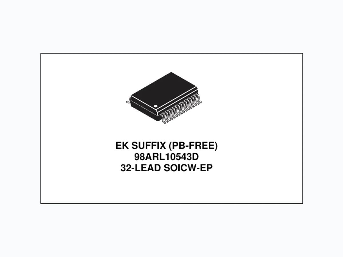
Analog Integrated Circuit Device Data Freescale Semiconductor 23 33730 PACKAGING PACKAGE DIMENSIONS PACKAGING PACKAGE DIMENSIONS For the most current package revision, visit www.freescale.com and perform a keyword search using the 98ARL10543D listed below. Dimensions shown are provided for reference ONLY. EK SUFFIX (PB-FREE) 32-PIN SOICW - EP 98ARL10543D REVISION C
Analog Integrated Circuit Device Data
24 Freescale Semiconductor
PACKAGE DIMENSIONS (CONTINUED) PACKAGE DIMENSIONS (Continued) EK SUFFIX (PB-FREE) 32-PIN SOICW - EP 98ARL10543D REVISION C
Analog Integrated Circuit Device Data Freescale Semiconductor 25 33730 PACKAGING PACKAGE DIMENSIONS (CONTINUED) PACKAGE DIMENSIONS (Continued) EK SUFFIX (PB-FREE) 32-PIN SOICW - EP 98ARL10543D REVISION C
26 Freescale Semiconductor
Table 11. Reference Documents
Analog Integrated Circuit Device Data Freescale Semiconductor 27 33730
REVISION HISTORY
REVISION DATE DESCRIPTION OF CHANGES 5.0 2/2009 • Initial Release 6.0 2/2010 • Updated resistors on the INV pin (page 2, 20, 21)
- Clarified REGON pin operation (page 3, 9, 11, 14)
- Added sensor supply max. slew rate (page 5,17)
- Clarified POR delay section with updated typical values (page 10,18)
- Modified the SW rise and fall time to V/ns (page 10)
- Provided a switching frequency equation (page 15)
- Updated the recommended compensation network values (page 20,21)
- Made format layout corrections 7.0 4/2010 • Corrected typographical error on Capacitor ( μF to nF) in Figures 8 and 9. 8.0 8/2010 • Added Note to page 4 (Pin Definitions) for Pins P1, P2 and P3.
- Revised paragraph in section; Programming Linear Regulator Output Voltage on page 18 9.0 8/2012 • Added part number MC33730EK to the Ordering Information table
- Added Device Variations on page 2
- Added REFERENCE SECTION on page 26
- Updated Freescale form and style
Document Number: MC33730 Rev. 9.0 Information in this document is provided solely to enable system and software implementers to use Freescale products. There are no express or implied copyright licenses granted hereunder to design or fabricate any integrated circuits based on the information in this document. Freescale reserves the right to make changes without further notice to any products herein. Freescale makes no warranty, representation, or guarantee regarding the suitability of its products for any particular purpose, nor does Freescale assume any liability arising out of the application or use of any product or circuit, and specifically disclaims any and all liability, including without limitation consequential or incidental damages. “Typical” parameters that may be provided in Freescale data sheets and/or specifications can and do vary in different applications, and actual performance may vary over time. All operating parameters, including “typicals,” must be validated for each customer application by customer’s technical experts. Freescale does not convey any license under its patent rights nor the rights of others. Freescale sells products pursuant to standard terms and conditions of sale, which can be found at the following address: store.esellerate.net/store/ Policy.aspx?Selector=RT&s=STR0326182960&pc. How to Reach Us: Home Page: freescale.com Web Support: freescale.com/support Freescale, the Freescale logo, AltiVec, C-5, CodeTest, CodeWarrior, ColdFire, C-Ware, Energy Efficient Solutions logo, Kinetis, mobileGT, PowerQUICC, Processor Expert, QorIQ, Qorivva, StarCore, Symphony, and V ortiQa are trademarks of Freescale Semiconductor, Inc., Reg. U.S. Pat. & Tm. Off. Airfast, BeeKit, BeeStack, ColdFire+, CoreNet, Flexis, MagniV , MXC, Platform in a Package, QorIQ Qonverge, QUICC Engine, Ready Play, SafeAssure, SMARTMOS, TurboLink, Vybrid, and Xtrinsic are trademarks of Freescale Semiconductor, Inc. All other product or service names are the property of their respective owners. © 2012 Freescale Semiconductor, Inc.