
DSTINIS400_08 MAXIM
Document overview
- Manufacturer or author: Provided By digicamel.com
- PDF pages: 12
Technical content
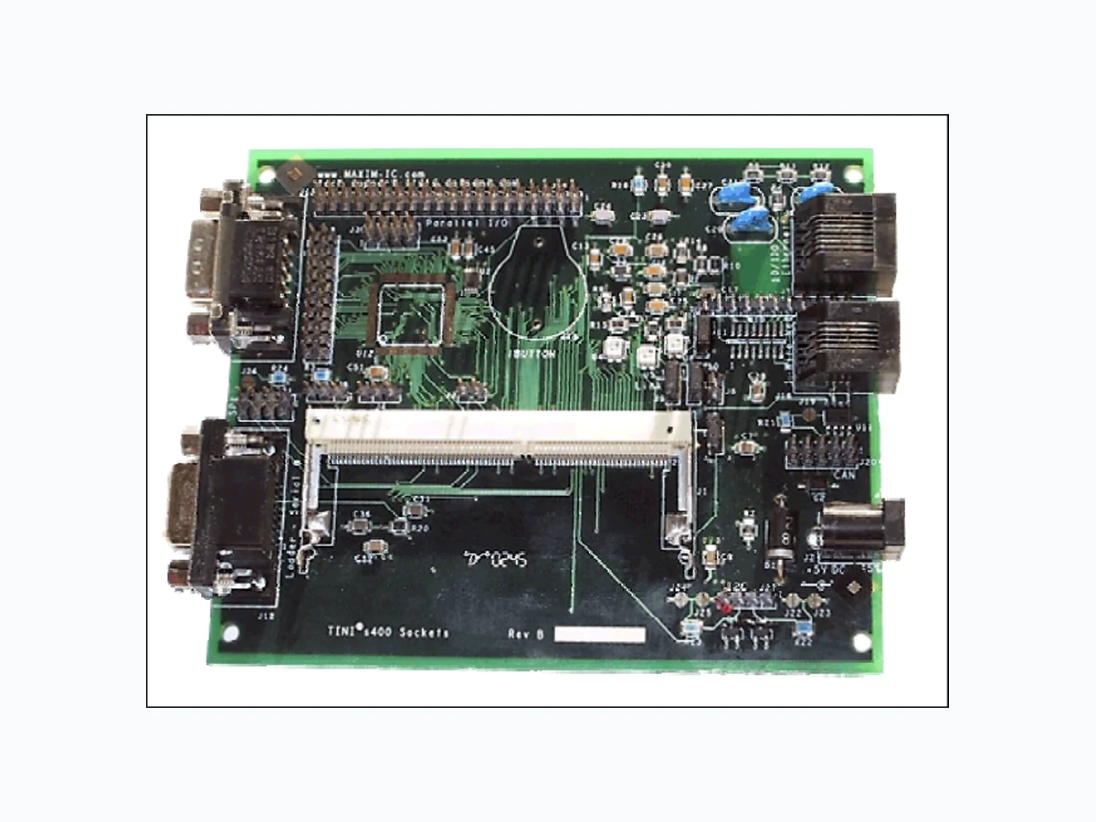
1 of 12 REV: 061608 GENERAL DESCRIPTION The TINI ® sockets boards are motherboards designed to host the corresponding TINI evaluation module. The combination of the two boards allows full evaluation of the features of the target microprocessor. To eval uate the DS80C400, you only need to order the DS80C400-KIT. To evaluate the DS80C410 or DS80C411, you must order both the DSTINIm410# and the DSTINIs400# and use them together. The DSTINIm410# is used to evaluate both the DS80C410 and DS80C411. Although various boards suppo rt different evaluation modules, the most popular is the DSTINIs400#. It includes a 144-pin SODIMM connector and provides 1-Wire ®, CAN 2.0B, serial, and a 10/100 Ethernet PHY for connecting the DSTINIm400# or DSTINIm410# to the physical world. The DSTINIm400# and DSTINIm410# are designed as modules to be plugged into the 144-pin SODIMM connector on the DSTINIs400#. All are fully assembled and, when used together in the correct combinations, they form a complete evaluation system for the network microcontroller. The DSTINIm400# and DSTINIm410# modules include the DS80C400 and DS80C410 network microcontrollers, a real-tim e clock, 1MB flash, 1MB static RAM, and support for an external Ethernet PHY for connecting to a wide variety of networks. Detailed information about the initial setup process and use of the TINI platform is contained in Application Note 612: Getting Started with the TINIm400 (DS80C400) Verification Module.
ORDERING INFORMATION
VOLTAGE* USED WITH MODULE DIMENSIONS DSTINIs400 Replaced with DSTINIs400# DSTINIs400# 5V DC regulated DSTINIm400 12cm x 10cm DSTINIs-005 5V DC regulated DSTINI1-1MG, DSTINI1-512 16cm x 10cm DSTINIs-006 9V to 18V DC DSTINI1-1MG, DSTINI1-512 16cm x 10cm Note: The DSTINIm400 is an evaluation board and is only tested to prototype standards. It is not tested for use in a production product. *The user must supply an external power supply. # Denotes a RoHS-compliant device that may include lead that is exempt under the RoHS requirements.
FEATURES
Hosts the TINI Runtime Environment in Validated Hardware Design (in Conjunction with the DSTINIm400) 10/100 Base-T Ethernet Port Two Serial Ports Dual 1-Wire Network Ports CAN 2.0B Port 5.0V Single-Supply Operation (DSTINIm400) Fully Assembled and Tested Design COMPONENT LIST DESIGNATION QTY DESCRIPTION C1 1 47pF capacitor (1206) C2, C4, C5, C6 4 47μF tantalum capacitors (3528-21) C3, C7, C9, C13, C15, C26, C28, C30, C38 9 100nF capacitors (1206) C12, C14, C17, C19, C25, C27, C29, C33, C37 9 10nF capacitors (1206) C8 1 220nF, 16V capacitor (1206) C10, C31, C32, C34, C35, C36 6 1.0μF capacitors (1206) C11 1 4.7μF capacitor (1206) DSTINIs400/DSTINIs-00x Sockets Evaluation Board www.maxim-ic.com TINI and 1-Wire are registered trademarks of Maxim Integrated Products, Inc.
DSTINIs400/DSTINIs-00x Sockets Evaluation Board 2 of 11 COMPONENT LIST (continued) DESIGNATION QTY DESCRIPTION C16, C18 2 270pF capacitor (1206) C20, C21, C22 3 1nF, 2kV radial capacitors (ceramic disk) C23, C24 2 27pF capacitors (1206) C40 1 0.10μF ±10%, 50V capacitor (1206) D1 1 1N5908 D0-201 D2 1 BAT54 SOT23 D3, D4 2 BAT54S SOT23 J1 1 SODIMM144 Molex 54698-7000 J2 1 2.5mm center, 5.5mm outside barrel connector J3–J6, J20, J21, J27 7 Dual-row connectors, 0.025 square pins J7 1 RJ-45 modular jack J9, J10, J11 3 3 x 1-pin headers, 0.1 centers J12 1 DB9 serial female J13 1 DB9 serial male J14 1 Pad jumper J16 1 RJ11 modular jack L1 1 22μH inductor Q1 1 BSS84 SIPMOS FET SOT23 R1 1 205kΩ ±1% resistor (1206) R2 1 121kΩ ±1% resistor (1206) R3 1 10kΩ ±5% resistor (1206) R4–R7, R8, R10, R11, R12 8 49.9Ω ±1% resistors (1206) R13, R9 2 47Ω resistor (1206) R14 1 22.1kΩ ±1% resistor (1206) R15, R17, R18 3 220Ω resistors (1206) DESIGNATION QTY DESCRIPTION R16 1 10kΩ resistor (1206) R19 1 Pad jumper R20 1 47kΩ resistor (1206) R21 1 124Ω ±1% resistor (1206) R22, R23 2 1kΩ resistor (1206) R24 1 10kΩ resistor (1206) T1 1 BelFuse S558-5999-T7 transformer U1 1 MAX1692 PWM step-down regulator U3 1 Intel LXT972ALC Ethernet PHY U4, U5, U6 3 Dialight 597-7741 LED U7 1 MAX560CAI transceiver U8 1 DS2480B serial 1-Wire line driver U9 1 DS9502 ESD protection diode U11 1 65HVD230D CAN transceiver Y1 1 25.000MHz, HC49US Z1, Z2, Z3 3 Ferrite bead, Fair-Rite 2512067007Y3 UNPOPULATED COMPONENTS J15 1 DS9094F i Button® Clip J18, J28, J29, J30 1 Not used U2 1 MAX1792EUA18 linear regulator U10 1 DS2408 1-Wire 8-channel addressable switch U12 1 Not used JUMPERS (DSTINIs400) Network Boot Jumper (J3) JUMPER CONFIGURATION 1-2 DS80C400 attempts to boot through Ethernet using DHCP and TFTP DTR Reset Jumper (J14) JUMPER CONFIGURATION 1-2 DTR reset communicates with the DS80C400 loader application. Quiet Boot Jumper (J5) JUMPER CONFIGURATION 1-2 DS80C400 boots without sending loader information to serial port. iButton is a registered trademark of Maxim Integrated Products, Inc.
DSTINIs400/DSTINIs-00x Sockets Evaluation Board 3 of 11 DSTINIs400 Ethernet Configuration Jumpers (J9, J10, J11) AUTO- NEGOTIATION SPEED (Mbps) DUPLEX J9 J10 J11 Half 2-3 (L) 1-2 (H) 2-3 (L) Disabled Half 1-2 (H) 2-3 (L) 2-3 (L) 100 Only Full/Half 1-2 (H) 2-3 (L) 1-2 (H) Half Only 1-2 (H) 1-2 (H) 2-3 (L) Enabled 10/100 Full or Half 1-2 (H) 1-2 (H) 1-2 (H) PIN HEADERS CONNNECTOR DESCRIPTION J18 Recreated I/O Port. Latched from 1-Wire bus. Requires installation of DS2408. See schematic. J20 CAN Bus. See schematic for pinout. J21 SPI™ Bus. See schematic for pinout. Alternately provides connection to P5.4–P5.7 J27 I2C Bus. See schematic for pinout. Alternately provides connection to P1.0 and P1.1. J28, J29, J30 Unused. No user-accessible pins available. QUICK START Recommended Equipment The sockets board requires an external power supply and cables as needed to ac cess the desired features of the board. The 5V DC power supply is mandatory, but the other cables are required only if that feature is to be used. The specific example shown here is for a DSTINIm400#/DSTINIs400# system. Hardware: 5V DC Power Supply Input Voltage: per customer requirements Output Voltage: 5V DC ±10% Output Current: >150mA Polarization: Positive Center Example: Digi-Key (www.digikey.com) part number T309-P6P-ND (110V input), 5V DC power Ethernet Cable: Note: There are two types of Ethernet cable. For connection to a router or hub, use a standard "straight-through" Ethernet cable. For direct connection to an Ethernet port on the back of a PC, use a "crossover" Ethernet cable. A crossover cable is specially made for two-computer networking. These cables can be purchased from almost any computer or electronics store. Example (straight-through): Radio Shack (www.radioshack.com) Cat 5E (3ft) Network Cable, part number 278- 1763 Example (crossover): Radio Shack Cat 5E (3m) Crossover Cable, part number 278-2011 RS-232C Serial Cable (DB9 Male to DB9 Female): This cable is straight-through, not a null-modem (crossover). These cables can be purchased from any computer or electronics store.
DSTINIs400/DSTINIs-00x Sockets Evaluation Board 4 of 12 Important Note Regarding U12 Component U12 is not placed on the product as supplied by Maxim, nor is it available for sale from Maxim. Inclusion of this component and related circuitry in the schematic is intended to demonstrate one method to add I/O expansion capability to the DSTINIs400, but the implementation details are left to the user; any modification of the product is not guaranteed or supported by Maxim. For more information on the possible uses of component U12, refer to Application Note 3664: Expanding TINI’s I/O Capability and Application Note 3412: TINIs400 External Serial Port Reference Design. MORE INFORMATION TINI platform details can be found at www.maxim-ic.com/TINI. The TINI Specification and Developer’s Guide (Addison-Welsey, 2001) is an invaluable resource when developing with the TI NI platform. Download a free copy from our website at www.maxim-ic.com/TINIguide. ADDITIONAL RESOURCES For detailed information about the initial setup and use of the TINI platform, refer to Application Note 612: Getting Started with the TINIm400 (DS80C400) Verification Module at www.maxim-ic.com/AN612. DS80C400 Network Microcontroller Data Sheet: www.maxim-ic.com/DS80C400 DS80C410 Networked Microcontroller Data Sheet: www.maxim-ic.com/DS80C410 DS80C400 Evaluation Kit (DS80C400-KIT): www.maxim-ic.com/DS80C400-KIT DSTINIm400 Networked Microcontroller Evaluation Board: www.maxim-ic.com/DSTINIm400 DSTINIm410 Networked Microcontroller Evaluation Board: www.maxim-ic.com/DSTINIm410 Microcontroller Website: www.maxim-ic.com/microcontrollers SPI is a trademark of Motorola, Inc.
DSTINIs400/DSTINIs-00x Sockets Evaluation Board 5 of 12 Maxim/Dallas Semiconductor cannot assume responsibility for use of any circuitry other than circuitry entirely embodied in a Maxim/Dallas Semiconductor product. No circuit patent licenses are implied. Maxim/Dallas Semiconductor reserves the right to change the circuitry and specifications without notice at any time. Maxim Integrated Products, 120 San Gabriel Drive, Sunnyvale, CA 94086 408-737-7600 © 2008 Maxim Integrated Products The Maxim logo is a registered trademark of Maxim Integrated Products, Inc. The Dallas logo is a registered trademark of Dallas Semiconductor Corporation.
REVISION HISTORY
Updated the Component List. 1, 2
100906 Replaced the Auto Negotiation Jumper (J9), 10/100Mb Ethernet Jumper
(J10), and Full-Duplex Jumper (J11) sections with the DSTINIs400 Ethernet Configuration Jumpers (J9, J10, J11) section. Added “#” to the end of DSTINIs400 references 1, 3
121406 Updated Ordering Information table and added note that the DSTINIm400 is
only tested to prototype standards. 1 070507 Changed the DTR Reset Jumper (J4) to DTR Reset Jumper (J14) section. 2
061608 In the Component List, changed the description for C2, C4, C5, C6; added
“(ceramic disk)” to C20, C21, C22 description. 1, 2
TxD[3:0] TxClk RxDV RxClk RxEr RxD[3:0] COL CRS MDC MDIO D[7:0] Local1W nWr nRd ALE nPSEn A16 A17 A18 A19 A20 A21 nPCE[3:0] nCE[7:3] A2 A1 A3 A0 P67 P66 P50 P51 P52 P53 P30 P31 P32 P33 P10 P11 P12 P13 P14 P15 P16 P17 Title Size Document Number Rev Date: Sheet o f TINIs400 C TINIm400 Socket Board: TINI Module Connector B 1 7Wednesday, May 21, 2003 Copyright (C) 2003 Dallas Semiconductor / Maxim J1 DIMM144 GND1 1 GND2 2 VCC3 3 VCC4 4 A13 5 nRstIn 6 A16 7 nRam2En 8 A15 9 A8 10 A14 11 A9 12 A17 13 A11 14 A20 15 nPSEN 16 A19 17 A10 18 D6 19 D7 20 D5 21 D3 22 D4 23 nFlashEn 24 D2 25 A0 26 D1 27 A4 28 D0 29 P1.4 30 A3 31 P1.5 32 A2 33 nRam1En 34 A1 35 P1.3 36 A12 37 P1.2 38 P1.6 39 P1.1 40 P1.7 41 P1.0 42 nRstOut 43 nEA 44 CRS 45 TxEn 46 COL 47 RxEr 48 RxDV 49 MDC 50 MDIO 51 GND52 52 GND53 53 TxD.3 54 TxD.2 55 TxD.1 56 TxD.0 57 GND58 58 GND59 59 TxClk 60 RxClk 61 GND62 62 GND63 63 RxD.0 64 RxD.1 65 RxD.2 66 RxD.3 67 GND68 68 GND69 69 NC70 70 P3.0 71 ALE 72 P3.1 73 P5.3 74 P3.2 75 nPCE1 76 NC77 77 nPCE3 78 P3.3 79 nPCE0 80 NC81 81 nPCE2 82 nWr 83 NC84 84 nRd 85 NC86 86 P5.2 87 NC88 88 NC89 89 NC90 90 NC91 91 NC92 92 NC93 93 NC94 94 P5.1 95 P5.0 96 A18 97 nCE3 98 nCE2 99 nCE1 100 nCE0 101 P6.7 102 P6.6 103 A21 104 nCE7 105 nCE6 106 nCE5 107 nCE4 108 A5 109 NC109 110 A6 111 NC112 112 A7 113 NC114 114 NC115 115 Local1W 116 NC117 117 vPullup 118 NC119 119 NC120 120 NC121 121 NC122 122 NC123 123 NC124 124 NC125 125 NC126 126 NC127 127 NC128 128 NC129 129 NC130 130 NC131 131 NC132 132 NC133 133 NC134 134 NC135 135 NC136 136 NC137 137 NC138 138 NC139 139 NC140 140 VCC141 141 VCC142 142 GND143143 GND144144
Date: Sheet o f TINIs400 C TINIm400 Socket Board: Power and Internals A 2 7Thursday, May 22, 2003 Copyright (C) 2003 Dallas Semiconductor / Maxim
5 VDC +-5% INPUT
+ C4 47uF 3Pin 1N5908 0.1 uF BSS84 0.22 uF + C6 47uF 10 K 22 uH Bead 205K 1% MAX1692 IN 1 LIM 6 SHDN 8 REF 4 BP 2 LX 9 FB 5SYNC/PWM 7 GND 3 PGND 10 121K 1% 0.1 uF 47 pF 3Pin 0.1 uF + C2 47uF + C5 47uF C11 4.7uF 2Pin 87-72010-004 MAX1792EUA18 IN2 2 RST 3 SHDN 4 OUT1 8 OUT2 7 SET 6 GND 5 IN1 1 C10 1.0uF
TxD[3:0] COL MDC CRS RxClk TxEn MDIO RxDV RxD[3:0] TxClk nRstOut Title Size Document Number Rev Date: Sheet o f TINIs400 C TINIm400 Socket Board: Ethernet A 3 7Wednesday, May 21, 2003 Copyright (C) 2003 Dallas Semiconductor / Maxim A_Gnd A_Gnd 10/100-BASE-T ETHERNET PHY MODE CONFIGURATION PHY MODE CONFIGURATION PHY MODE CONFIGURATION DECOUPLING CAPS FOR U2 A_Gnd A_Gnd 1% 1% 1% 1% C14 0.01 uF C15 0.1 uF C20 0.001 uF, 2 kV R17 220 C16 270 pF C21 0.001 uF, 2 kV C18 270 pF R16 10 K C19 0.01 uF 597-7741 1 2 C22 0.001 uF, 2 kV
25.000 MHz
TX_EN 56 TX_CLK 55 TX_ER 54 RX_ER 53 RX_CLK 52 VCCD 51 GND12 50 RX_DV 49 RXD0 48 RXD1 47 RXD2 46 RXD3 45 MDC 43 MDIO 42 GND11 41 VCCIO2 40 PWRDWN 39 LED_CFG1 38 LED_CFG2 37 LED_CFG3 36 TEST1 35 TEST0 34 PAUSE 33 C23 27 pF R13 47 C24 27 pF R15 220 49.9 1% R10 49.9 1% J10
3 Pin
0.01 uF R14
22.1 K 1%
0 Ohm
0.1 uF R18 220 49.9 C27 0.01 uF 49.9 49.9 0.1 uF 49.9 RJ-45 C17 0.01 uF R11 49.9 1% C29 0.01 uF R12 49.9 1% C28 0.1 uF Z2 BEAD Z3 BEAD C12 0.01 uF R25 Option C13 0.1 uF Pad R9 47 J11 S558_5999_T7 710
DCD4 DCD4_232 CTS4_232 RX4_232 TX4_232 DTR4_232 RTS4_232 TX0_232 RX0_232 DTR0_232 VCC3 P31 P15 P16 P67 P30 P66 P33 P14 nRstIn nShDn Title Size Document Number Rev Date: Sheet o f TINIs400 C TINIm400 Socket Board: Internal Serial Ports 0 and 4 A 4 7Wednesday, May 21, 2003 Copyright (C) 2003 Dallas Semiconductor / Maxim SERIAL PORT 0 SERIAL PORT 4 CONNECT TO ENABLE RESET FROM DTR J12 DB9 FEMALE (DCE) J13 DB9 MALE (DTE) + C31 1 uF C33 0.01uF R20 47K C34 1 uF MAX560CAI C1+ 12 C1- 14 T1IN 7 T2IN 6 T3IN 20 T4IN 21 R1OUT 8 R2OUT 5 R3OUT 26 R4OUT 22 R5OUT 19 V+ 13 VCC 11 EN 24 SHDN 25 C2+ 15 C2- 16 GND 10 V- 17 T1OUT 2 T2OUT 3 T3OUT 1 T4OUT 28 R1IN 9 R2IN 4 R3IN 27 R4IN 23 R5IN 18 J14 PAD JUMPER C32 1 uF C35 1 uF C36 1 uF
Date: Sheet o f TINIs400 C TINIm400 Socket Board: External 1-Wire Interface and DS2408 A 5 7Wednesday, May 21, 2003 Copyright (C) 2003 Dallas Semiconductor / Maxim I-BUTTON CLIP EXTERNAL 1-WIRE
8 I/O LINES WITH STROBE
0.01 uF J18 11x1 C38 0.1 uF J15 DS9094F DS2480B GND 1VDD 4 TXD 7 RXD 8 POL 6 NC 3 OWIO 2 VPP 5 BAT54 U10 DS2408 NC1 1 NC15 15 NC16 16 VCC 3 OWIO 4 GND 5 STRB 10 P0 2 P1 14 P2 13 P3 12 P4 11 P5 9 P6 8 P7 7 + C39 47uF J16 RJ11
nPCE[3:0] nShDn Title Size Document Number Rev Date: Sheet o f TINIs400 C TINIm400 Socket Board: Other I/O A 6 7Wednesday, May 21, 2003 Copyright (C) 2003 Dallas Semiconductor / Maxim I2C BUS CAN BUS CONNECT TO TERMINATE SPI BAT54S 1 2 R22 1 K J19 R21 124 J21 4x2 1 2 3 4 5 6 7 8 R23 1 K C40 0.1 uF J26 Pad Jumper J20 5x2 J27 4 HEADER PINS, 0.1" R24 10K J22 J23 J24 U11 SN65HVD230 VCC 3 GND 2 RS 8 CANH 7 CANL 6 TXD 1 RXD 4 VREF 5 J25 BAT54S 1 2
D[7:0] ALE nRstOut nPSEn nRd nWr nCE[7:3] nExtInt P53 P17 A16 A17 A18 A19 A20 A21 Title Size Document Number Rev Date: Sheet o f DSTINIs400 C Programmable I/O A 7 7Wednesday, May 21, 2003 Copyright (C) 2003 Dallas Semiconductor / Maxim each U1 V33 connection One 10 nF ceramic capacitor for each U1 V18 connection Expanded I/O User I/O One 10 nF ceramic capacitor for One 100 nF ceramic capacitor for each U1 V33 connection One 100 nF ceramic capacitor for each U1 V18 connection J29