
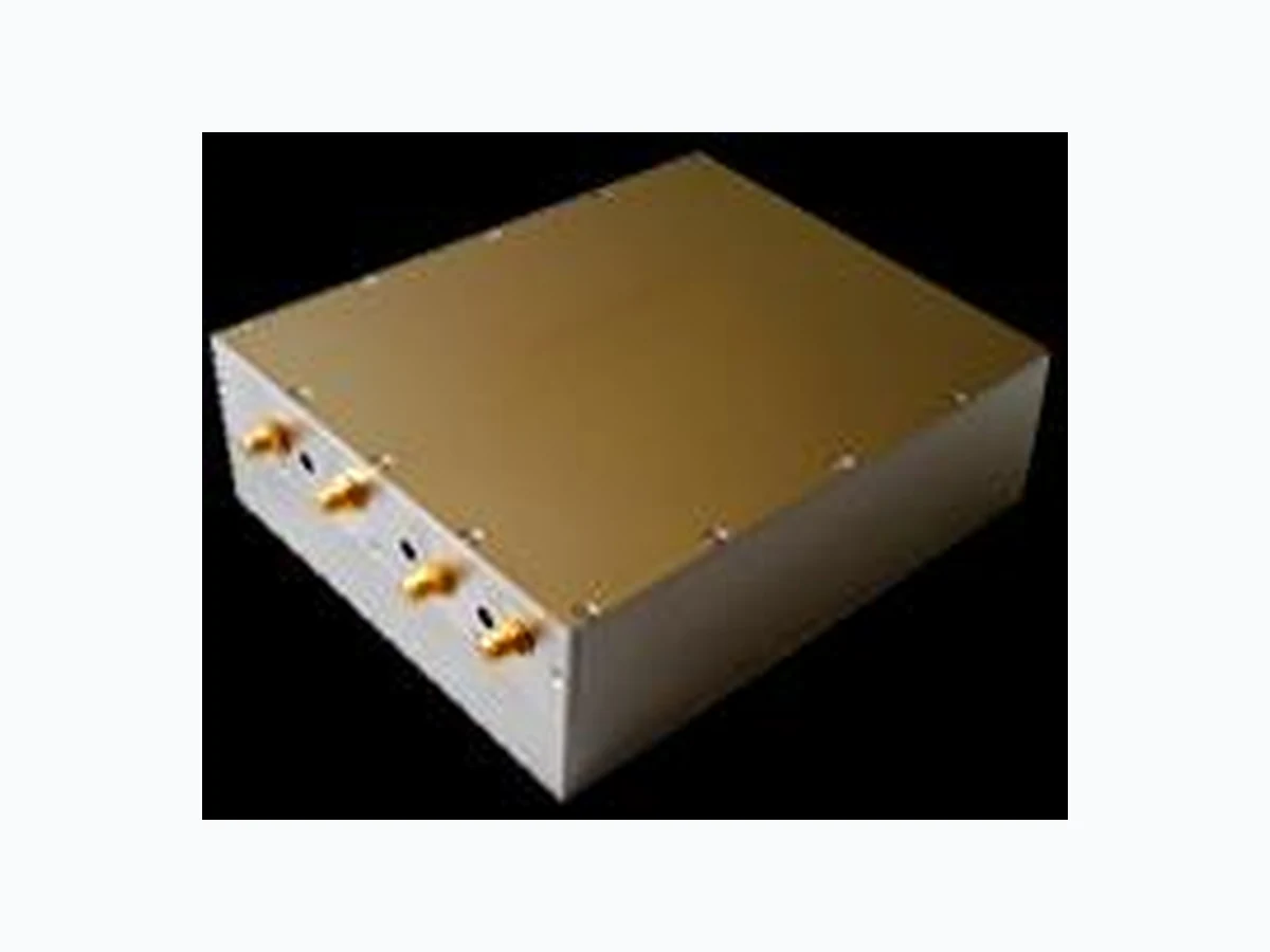
DSH01 TEMEX
Document overview
- Manufacturer or author: Provided By www.digicamel.com(FREE DATASHEET DOWNLOAD SITE)
- PDF pages: 8
Technical content
DIGITAL SYNTHESIZER MODULE | SYSTEM SOLUTIONS Issue: A0, 24 Sep 2018 Copyright © 2018 Rakon Limited. All rights reserved Specifications subject to change without notice Page 1 of 8 www.rakon.com Specific requests can be emailed to Rakon: hirel@rakon.com DS H01 The DS H01 is a high performance dual digital synthesizer with wide output bandwidth specially designed for Defense applications where generation of wideband ultra-low noise signals along with very fast switching times are needed. This module has two independent outputs with more than 500 MHz bandwidth and a Spurious -Free Dynamic Range (SFDR non-harmonics) better than 70 dBc. Each output can change its frequency in less than 10 ns. Internally, both outputs can be used to feed an IQ modulator to obtain a 1 GHz bandwidth signal in the range of 3.5 GHz. Clocks may be internal or can be provided by the user in case of coherent signal generation with the rest of the user’s system is required. Several IOs are available (differential and single ended) to allow the user to interface the unit with the other system signals in a very straight- forward way. All IOs are electrically protected in order to support harsh environments. DS H01 has a very high speed Field -Programmable Gate Array (FPGA) inside to link us er interface to the output signal generation allowing the customer to have a huge flexibility. A Joint Test Action Group (JTAG) connector is available to interface with the FPGA. Technical Description DS H01 is composed of 3 main functional blocks
- Interface: I/Os are protected and converted to different standards.
- Signal generator: High bandwidth signal generator with an integrated IQ modulator
- User application: User specific application linking the two others functional blocks Fig. 1: Functional Block Diagrams Features Applications 174 x 131 x 54 mm Frequency output bandwidth: › Dual channel: 0.1 – 500 MHz › Single channel: LO – 500 MHz to LO – 500 MHz (internal LO = 3.5 GHz) Phase Noise @ 320 MHz: › 100 Hz offset: -98 dBc/Hz typ. › Noise floor: -154 dBc/Hz typ. Chirp generation Frequency switch time: 10 ns max. Wideband SFDR for IQ output: 70 dBc typ. (non-harmonics) Frequency tuning resolution: 7.1 µHz typ. FSK, PSK, QAM modulations RADAR LO frequency generation Pulse compression RADAR RF pulse expander FMCW RADAR Electronic counter- countermeasures (ECCM) Frequency hopping Signal Generator Interfaces User Application (FPGA) DDS I I Output 100 kHz – 500 MHz CLK Mod Mod Output 3 – 4 GHz DDS Q Q Output 100 kHz – 500 MHz TTL USB RS-485 JTAG CLK DDS
DIGITAL SYNTHESIZER MODULE | SYSTEM SOLUTIONS Issue: A0, 24 Sep 2018 Copyright © 2018 Rakon Limited. All rights reserved Specifications subject to change without notice Page 2 of 8 www.rakon.com Specific requests can be emailed to Rakon: hirel@rakon.com Interface I/O
- 12 TTL inputs or 6 RS-422 differential inputs
- 4 TTL outputs or 2 RS-422 outputs
- 1 USB interface
- 1 JTAG interface
- 1 BITE (Built-In Test Equipment) output BITE signal is controlled by the user application and is OR’ed with the board power supply status. This signal can be configured as open-drain or as dry contact. Signal Generator The unit generates the output signal based on a DDS (Direct Digital Synthesizer) scheme. A sine waveform is stored in a LUT (Look-Up Table) and then is swept to generate the output signal. The main advantage of this architecture is the speed: output signal can change its frequency in less than 10 ns. Each DDS block is composed of a DDS Core Block and a high speed DAC to perform the digital to analog conversion. The core of the DDS is implemented inside the FPGA and interacts with the User Application using 3 data lines that allow to change frequency, phase and gain on real-time. This block also interacts with a high speed DAC which is responsible of the digital to analog conversion. Fig. 2: DDS Core Block Diagram Fig. 3: IQ Modulator Finally, the user can either route each DDS directly to the module’s output or fed them to an internal IQ modulator for up conversion purpose. Signal Generator I Output 100 kHz – 500 MHz CLK Mod Mod Output 3 – 4 GHz Q Output 100 kHz – 500 MHz DDS IQ I/Q Output 100 kHz – 500 MHz FPGA DDS Core Gain Phase Frequency DAC
DIGITAL SYNTHESIZER MODULE | SYSTEM SOLUTIONS Issue: A0, 24 Sep 2018 Copyright © 2018 Rakon Limited. All rights reserved Specifications subject to change without notice Page 3 of 8 www.rakon.com Specific requests can be emailed to Rakon: hirel@rakon.com User Application Having the Frequency, Phase and Gain available as parameters to the Customer, opens a wide spectrum of solutions. Here are some examples of the product capabilities Fig. 4: Chirp Generator Chirp Generator: A Chirp is stored in a LUT and swept using a Controller block. This block is triggered by an external signal (normally the main ON/OFF transmission Radar’s signal). A correction block is added in order to compensate Phase and Gain as frequency changes. This compensation is done real-time. Fig. 5: FSK Modulator FSK Modulator: Digital signal to be modulated is routed using one of the differential interfaces. A controller block chooses the transmitting frequency from the value of the input. Fig. 6: The figure below shows a capture of an FSK modulated pulse of 8 µs. Bit time is approximately 250 ns. FPGA DDS Core Phase DAC Corrections Gain Controller Mod Input Trigger Frequency FPGA DDS Core Phase DAC Corrections Gain Controller RS-422 Trigger Frequency
DIGITAL SYNTHESIZER MODULE | SYSTEM SOLUTIONS Issue: A0, 24 Sep 2018 Copyright © 2018 Rakon Limited. All rights reserved Specifications subject to change without notice Page 4 of 8 www.rakon.com Specific requests can be emailed to Rakon: hirel@rakon.com Fig. 7: Sectorized Radar signal generator Sectorized Radar Signal generator (S Band): As the previous cases, a trigger signal is used to start emission. Two channels are used to upconvert the output using the IQ Modulator. The antenna encoder is fed to module in order to have a sectorized configuration. An SPI interface is also provided to let the user choose the desired waveform. Output is directly upconverted to the Radar’s operating frequency. Fig. 8: Clocking architecture Clocking: The module proposes several clocking schemes. An internal 20 MHz oscillator provides the reference to two PLLs. One have 2 GHz VCO for the DDS clock and the other 3.5 GHz VCO for the IQ Modulator. However, the reference for each PLL can be provided externally in case of coherent generation. Finally, the user can input directly the clock without using the internal PLLs. All these clocking possibilities are set using the User application providing the user a very flexible way to adapt clocking to its own final application. CLK Mod FPGA DDS Core Phase DAC Correction s Gain Antenna Encoder Trigger Frequency Chip LUT Phase + 90° DAC Gain DDS Core Frequency Controller SPI Interface Output Corrections CLK Mod CLK DDS VCO
2 GHz
20 MHz
3.5 GHz PLL J22 Clk Mod Ext
DIGITAL SYNTHESIZER MODULE | SYSTEM SOLUTIONS Issue: A0, 24 Sep 2018 Copyright © 2018 Rakon Limited. All rights reserved Specifications subject to change without notice Page 5 of 8 www.rakon.com Specific requests can be emailed to Rakon: hirel@rakon.com 1. Environmental Conditions1 Parameter Condition / Remarks Min. Typ. Max. Unit Temperature operating -25 +70 °C Temperature storage -40 +85 °C Humidity operating @ 30 °C, (non-condensing) 95 % RH Shock 11 ms, 3 axes, 2 dir, half sine pulse 30 g Random Vibration 20 to 500 Hz, 3 axes 0.1 g2/Hz EMI - EMC In accordance with MIL-STD 461 F 2. Electrical Interface Parameter Condition / Remarks Min. Typ. Max. Unit Supply voltage 11 16 V Supply current @ Power supply = 15 V 1300 mA RF IN signal Type Maximum input level Impedance Single 1.3 : 1 dBm VSWR RF OUT signal Type Output level Impedance Single 1.3 : 1 dBm VSWR User input Type Impedance RS422 / TTL 120 Ω User output type RS422 / TTL Bite output type Open drain / Dry Contact 3. Electrical Characteristics Parameter Condition / Remarks Min. Typ. Max. Unit IQ output BW 0.1 500 MHz IQ modulator output BW With internal Modulator clock 3000 4000 MHz DAC clock input frequency 1500 2000 MHz Modulator clock input frequency 3200 3800 MHz Frequency tuning resolution 7.1 µHz Wideband SFDR @ IQ output 70 dBc Wideband SFDR @ IQ modulator output 40 dBc Phase accuracy 1 mrad
1 Procedures and conditions refer to MIL-STD-810G
DIGITAL SYNTHESIZER MODULE | SYSTEM SOLUTIONS Issue: A0, 24 Sep 2018 Copyright © 2018 Rakon Limited. All rights reserved Specifications subject to change without notice Page 6 of 8 www.rakon.com Specific requests can be emailed to Rakon: hirel@rakon.com 4. IQ Output Performance Fig 9: Signal Tone @ 100 MHz Fig 10: Signal Tone @ 200 MHz Fig 11: Signal Tone @ 300 MHz Fig 12: Signal Tone @ 400 MHz Fig 11: Signal Tone @ 500 MHz
DIGITAL SYNTHESIZER MODULE | SYSTEM SOLUTIONS Issue: A0, 24 Sep 2018 Copyright © 2018 Rakon Limited. All rights reserved Specifications subject to change without notice Page 7 of 8 www.rakon.com Specific requests can be emailed to Rakon: hirel@rakon.com 5. Phase Noise (Typical value @ 25°C) Parameter 320 MHz2 480 MHz2 4000 MHz3 Unit Test Condition / Description
100 Hz offset -98 -96 -75 dBc/Hz
1 kHz offset -110 -104 -80 dBc/Hz 10 kHz offset -130 -126 -110 dBc/Hz 100 kHz offset -146 -142 -135 dBc/Hz
1 MHz offset -154 -152 -145 dBc/Hz
- Phase Noise Performance Fig 14: Phase Noise @ 320 and 480 MHz Fig 15: Phase Noise @ 4000 MHz 2 Test condition: With internal DAC clock. 3 Test condition: With internal DAC clock and modulator clock.
DIGITAL SYNTHESIZER MODULE | SYSTEM SOLUTIONS Issue: A0, 24 Sep 2018 Copyright © 2018 Rakon Limited. All rights reserved Specifications subject to change without notice Page 8 of 8 www.rakon.com Specific requests can be emailed to Rakon: hirel@rakon.com 7. Model Outline and Mechanical Features Fig 16: DS H01 Model Outline Drawing Model outline With connectors: 174x131x54 mm3 typ. Without connectors: 166x131x54 mm3 typ. Unit weight 0.6 kg max. Material AG4.5MC Treatment Ni20 / Zn1 Screws A4-70 stainless steel 8. Interfaces Description and Pin-out Pin Connections Description J8 Mod Output / I Output IQ Modulator Output or I Output
3 GHz ~ 4 GHz or 100 kHz ~ 500 MHz; AC, 50 Ω, SMA connector
100 kHz ~ 500 MHz; AC, 50 Ω, SMA connector J20 CLK DAC Ext Clock input for DDS or reference clock
2 GHz or 20 ~ 250 MHz; AC, 50 Ω, SMA connector
J22 CLK Mod Ext Clock input for IQ Modulator or reference clock 3200 ~ 3800 MHz or 20 ~ 250 MHz; AC, 50 Ω, SMA connector P1-1, P1-22 VCC 15 V power supply input P1: MIL-C-24308 25-pin SubD Connector P1-14, P1-15 GND POW Power supply ground P1-3 to P1-5 P1-7 to P1-9 P1-16 to P1-19 P1-21, P1-22 CTRL Inputs Input signals for control RS-422 compatible input / TTL input; 120 Ω differential impedance P1-10, P1-11 P1-23, P1-24 CTRL Outputs Output signals for control RS-422 compatible output / TTL output P1-12, P1-25 BITE BITE output Open drain or dry contact; Indicates unit OK or NOK P1-6, P1-13 GND Mechanical ground P3 JTAG JTAG interface for program download MOLEX type 87833-1420 connector