
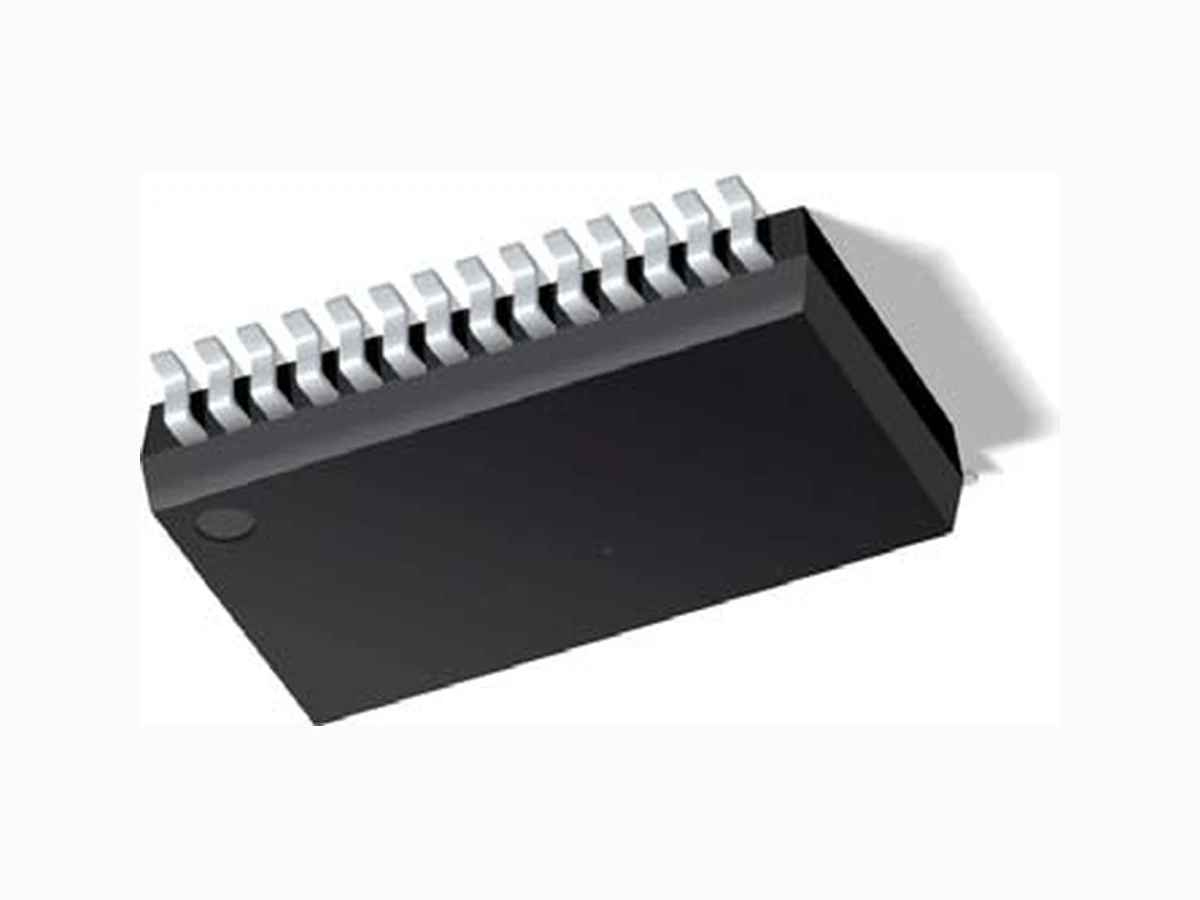
24-Bit, 192kHz Sampling, Advanced Segment, Audio Stereo DAC datasheet (Rev. B)
Document overview
- Manufacturer or author: Texas Instruments, Incorporated [SLES072,B]
- PDF pages: 57
Technical content
/C0068/C0083/C0068/C0049/C0055/C0057/C0049 SLES072B − MARCH 2003 − REVISED NOVEMBER 2006 /C0050/C0052/C0262/C0066/C0073/C0084/C0044 /C0049/C0057/C0050/C0262/C0107/C0072/C0122 /C0083/C0065/C0077/C0080/C0076/C0073/C0078/C0071/C0044 /C0065/C0068/C0086/C0065/C0078/C0067/C0069/C0068 /C0083/C0069/C0071/C0077/C0069/C0078/C0084/C0044 /C0065/C0085/C0068/C0073/C0079 /C0083/C0084/C0069/C0082/C0069/C0079 /C0068/C0073/C0071/C0073/C0084/C0065/C0076/C0262/C0084/C0079/C0262/C0065/C0078/C0065/C0076/C0079/C0071 /C0067/C0079/C0078/C0086/C0069/C0082/C0084/C0069/C0082
FEATURES
/C0068Supports both DSD and PCM Formats /C006824-Bit Resolution /C0068Analog Performance: − Dynamic Range: 113 dB − THD+N: 0.001% − Full-Scale Output: 2.1 V RMS (at Postamp) /C0068Differential Voltage Output: 3.2 Vp-p /C00688× Oversampling Digital Filter: − Stop-Band Attenuation: –82 dB − Pass-Band Ripple: ±0.002 dB /C0068Sampling Frequency: 10 kHz to 200 kHz /C0068System Clock: 128, 192, 256, 384, 512, or 768 fS With Autodetect /C0068Accepts 16-, 20-, and 24-Bit PCM Audio Data /C0068PCM Data Formats: Standard, I2S, and Left-Justified /C0068DSD Format Interface Available /C0068Optional Interface to External Digital Filter or DSP Available /C0068TDMCA Interface Available /C0068User-Programmable Mode Controls: − Digital Attenuation: 0 dB to –120 dB, 0.5 dB/Step − Digital De-Emphasis − Digital Filter Rolloff: Sharp or Slow − Soft Mute − Zero Flag for Each Output/PCM and DSD Formats /C0068Dual Supply Operation: − 5-V Analog, 3.3-V Digital /C00685-V Tolerant Digital Inputs /C0068Small 28-Lead SSOP Package
APPLICATIONS
/C0068A/V Receivers /C0068SACD Players /C0068DVD Players /C0068HDTV Receivers /C0068Car Audio Systems /C0068Digital Multitrack Recorders /C0068Other Applications Requiring 24-Bit Audio
DESCRIPTION
The DSD1791 is a monolithic CMOS integrated circuit that includes stereo digital-to-analog converters and support circuitry in a small 28-lead SSOP package. The data converters use TI’s advanced segment DAC architecture to achieve excellent dynamic performance and improved tolerance to clock jitter. The DSD1791 provides balanced voltage outputs, allowing the user to optimize analog performance externally. The DSD1791 accepts PCM and DSD audio data formats, providing easy interfacing to audio DSP and decoder chips. The DSD1791 also accepts interface to external digital filter devices (DF1704, DF1706, PMD200). Sampling rates up to 200 kHz are supported. A full set of user-programmable functions is accessible through an SPI control port, which supports register write and readback functions. The DSD1791 also supports the time-division-multiplexed command and audio (TDMCA) data format. This integrated circuit can be damaged by ESD. Texas Instruments recommends that all integrated circuits be handled with appropriate precautions. Failure to observe proper handling and installation procedures can cause damage. ESD damage can range from subtle performance degradation to complete device failure. Precision integrated circuits may be more susceptible to damage because very small parametric changes could cause the device not to meet its published specifications. /C0080/C0082/C0079/C0068/C0085/C0067/C0084/C0073/C0079/C0078 /C0068/C0065/C0084/C0065 /C0105/C0110/C0102/C0111/C0114/C0109/C0097/C0116/C0105/C0111/C0110 /C0105/C0115 /C0099/C0117/C0114/C0114/C0101/C0110/C0116 /C0097/C0115 /C0111/C0102 /C0112/C0117/C0098/C0108/C0105/C0099/C0097/C0116/C0105/C0111/C0110 /C0100/C0097/C0116/C0101/C0046 /C0080/C0114/C0111/C0100/C0117/C0099/C0116/C0115 /C0099/C0111/C0110/C0102/C0111/C0114/C0109 /C0116/C0111 /C0115/C0112/C0101/C0099/C0105/C0102/C0105/C0099/C0097/C0116/C0105/C0111/C0110/C0115 /C0112/C0101/C0114 /C0116/C0104/C0101 /C0116/C0101/C0114/C0109/C0115 /C0111/C0102 /C0084/C0101/C0120/C0097/C0115 /C0073/C0110/C0115/C0116/C0114/C0117/C0109/C0101/C0110/C0116/C0115 /C0115/C0116/C0097/C0110/C0100/C0097/C0114/C0100 /C0119/C0097/C0114/C0114/C0097/C0110/C0116/C0121/C0046 /C0080/C0114/C0111/C0100/C0117/C0099/C0116/C0105/C0111/C0110 /C0112/C0114/C0111/C0099/C0101/C0115/C0115/C0105/C0110/C0103 /C0100/C0111/C0101/C0115 /C0110/C0111/C0116 /C0110/C0101/C0099/C0101/C0115/C0115/C0097/C0114/C0105/C0108/C0121 /C0105/C0110/C0099/C0108/C0117/C0100/C0101 /C0116/C0101/C0115/C0116/C0105/C0110/C0103 /C0111/C0102 /C0097/C0108/C0108 /C0112/C0097/C0114/C0097/C0109/C0101/C0116/C0101/C0114/C0115/C0046 Please be aware that an important notice concerning availability, standard warranty, and use in critical applications of Texas Instruments semiconductor products and disclaimers thereto appears at the end of this data sheet. /C0066/C0117/C0114/C0114/C0262/C0066/C0114/C0111/C0119/C0110 /C0080/C0114/C0111/C0100/C0117/C0099/C0116/C0115 /C0102/C0114/C0111/C0109 /C0084/C0101/C0120/C0097/C0115 /C0073/C0110/C0115/C0116/C0114/C0117/C0109/C0101/C0110/C0116/C0115 Copyright 2006, Texas Instruments Incorporated
/C0068/C0083/C0068/C0049/C0055/C0057/C0049 SLES072B − MARCH 2003 − REVISED NOVEMBER 2006 www.ti.com
ORDERING INFORMATION
PRODUCT PACKAGE PACKAGE CODE OPERATION TEMPERATURE RANGE PACKAGE MARKING ORDERING NUMBER TRANSPORT MEDIA DSD1791DB 28-lead SSOP 28DB –25°C to 85°C DSD1791 DSD1791DB Tube DSD1791DB 28-lead SSOP 28DB –25°C to 85°C DSD1791 DSD1791DBR Tape and reel ABSOLUTE MAXIMUM RATINGS over operating free-air temperature range unless otherwise noted(1) DSD1791 Supply voltage VCC F, VCC L, VCC C, VCC R –0.3 V to 6.5 V Supply voltage VDD –0.3 V to 4 V Supply voltage differences: VCC F, VCC L, VCC C, VCC R ±0.1 V Ground voltage differences: AGNDF, AGNDL, AGNDC, AGNDR, DGND ±0.1 V Digital input voltage PLRCK, PDATA, PBCK, DSDL, DSDR, DBCK, MS(2), MDI(2), MC, SCK, RST –0.3 V to 6.5 V Digital input voltageZEROL, ZEROR, MS (3), MDI(3) –0.3 V to (VDD + 0.3 V) < 4 V Analog input voltage –0.3 V to (VCC + 0.3 V) < 6.5 V Input current (any pins except supplies) ±10 mA Ambient temperature under bias –40°C to 125°C Storage temperature –55°C to 150°C Junction temperature 150°C Lead temperature (soldering) 260°C, 5 s Package temperature (IR reflow, peak) 260°C (1)Stresses beyond those listed under “absolute maximum ratings” may cause permanent damage to the device. These are stress ratings only, and functional operation of the device at these or any other conditions beyond those indicated under “recommended operating conditions” is not implied. Exposure to absolute-maximum-rated conditions for extended periods may affect device reliability. (2)Input mode (3)Output mode
ELECTRICAL CHARACTERISTICS
all specifications at TA = 25°C, VCC = 5 V, VDD = 3.3 V, fS = 44.1 kHz, system clock = 256 fS, and 24-bit data, unless otherwise noted PARAMETER DSD1791DB UNITPARAMETER MIN TYP MAX UNIT RESOLUTION 24 Bits DATA FORMAT (PCM Mode) Audio data interface format Standard, I2S, left justified Audio data bit length 16-, 20-, 24-bit selectable Audio data format MSB first, 2s complement fS Sampling frequency 10 200 kHz System clock frequency 128, 192, 256, 384, 512, 768 fS DATA FORMAT (DSD Mode) Audio data interface format DSD (direct stream digital) Audio data bit length 1 Bit fS Sampling frequency 2.8224 MHz System clock frequency 2.8224 11.2896 MHz
/C0068/C0083/C0068/C0049/C0055/C0057/C0049 SLES072B − MARCH 2003 − REVISED NOVEMBER 2006 www.ti.com ELECTRICAL CHARACTERISTICS (Continued) all specifications at TA = 25°C, VCC = 5 V, VDD = 3.3 V, fS = 44.1 kHz, system clock = 256 fS, and 24-bit data, unless otherwise noted PARAMETER TEST CONDITIONS DSD1791DB UNITPARAMETER TEST CONDITIONS MIN TYP MAX UNIT DIGITAL INPUT/OUTPUT Logic family TTL compatible VIH Input logic level VDCVIL Input logic level 0.8 VDC IIH Input logic current VIN = VDD 10 AIIL Input logic current VIN = 0 V –10 µA VOH Output logic level IOH = –2 mA 2.4 VDCVOL Output logic level IOL = 2 mA 0.4 VDC DYNAMIC PERFORMANCE (PCM MODE) (1) fS = 44.1 kHz 0.001% 0.002% THD+N at VOUT = 0 dB fS = 96 kHz 0.0015%THD+N at VOUT = 0 dB fS = 192 kHz 0.003% EIAJ, A-weighted, fS = 44.1 kHz 110 113 Dynamic range EIAJ, A-weighted, fS = 96 kHz 113 dBDynamic range EIAJ, A-weighted, fS = 192 kHz 113 dB EIAJ, A-weighted, fS = 44.1 kHz 110 113 Signal-to-noise ratio EIAJ, A-weighted, fS = 96 kHz 113 dBSignal-to-noise ratio EIAJ, A-weighted, fS = 192 kHz 113 dB fS = 44.1 kHz 106 110 Channel separation fS = 96 kHz 110 dBChannel separation fS = 192 kHz 109 dB Level linearity error VOUT = –120 dB ±1 dB DYNAMIC PERFORMANCE (DSD MODE) (1) (2) THD+N at VOUT = 0 dB 2.1 V rms 0.001% Dynamic range –60 dB, EIAJ, A-weighted 113 dB Signal-to-noise ratio EIAJ, A-weighted 113 dB ANALOG OUTPUT Gain error –8 ±3 8 % of FSR Gain mismatch, channel-to-channel –3 ±0.5 3 % of FSR Bipolar zero error At BPZ –2 ±0.5 2 % of FSR Differential output voltage (3) Full scale (0 dB) 3.2 V p-p Bipolar zero voltage (3) At BPZ 1.4 V Load impedance (3) R 1 = R2 1.7 kΩ (1)Dynamic performance and dc accuracy are specified at the output of the postamplifier as shown in Figure 33. Analog performance specifications are measured using the System Two/C0116 Cascade audio measurement system by Audio Precision/C0116 in the averaging mode. For all sampling-frequency operations, measurement bandwidth is limited with a 20-kHz AES17 filter. (2)Analog performance in the DSD mode is specified as the DSD modulation index of 100%. This is equivalent to PCM mode performance at 44.1 kHz and 64 fS. (3)These parameters are defined at the DSD1791 output pins. Load impedances, R1 and R2, are input resistors of the postamplifier. They are defined as dc loads. Audio Precision and System Two are trademarks of Audio Precision, Inc. Other trademarks are the property of their respective owners.
/C0068/C0083/C0068/C0049/C0055/C0057/C0049 SLES072B − MARCH 2003 − REVISED NOVEMBER 2006 www.ti.com ELECTRICAL CHARACTERISTICS (Continued) all specifications at TA = 25°C, VCC = 5 V, VDD = 3.3 V, fS = 44.1 kHz, system clock = 256 fS, and 24-bit data, unless otherwise noted PARAMETER TEST CONDITIONS DSD1791DB UNITPARAMETER TEST CONDITIONS MIN TYP MAX UNIT DIGITAL FILTER PERFORMANCE De-emphasis error ±0.1 dB FILTER CHARACTERISTICS-1: SHARP ROLLOFF Pass band ±0.002 dB 0.454 fSPass band –3 dB 0.49 fS Stop band 0.546 fS Pass-band ripple ±0.002 dB Stop-band attenuation Stop band = 0.546 fS –75 dBStop-band attenuation Stop band = 0.567 fS –82 dB Delay time 29/fS s FILTER CHARACTERISTICS-2: SLOW ROLLOFF Pass band ±0.04 dB 0.274 fSPass band –3 dB 0.454 fS Stop band 0.732 fS Pass-band ripple ±0.002 dB Stop-band attenuation Stop band = 0.732 fS –82 dB Delay time 29/fS s POWER SUPPLY REQUIREMENTS VDD Voltage range 3 3.3 3.6 VDC VCC Voltage range 4.5 5 5.5 VDC (1) fS = 44.1 kHz 6.5 8 IDD Supply current (1) fS = 96 kHz 13.5 mAIDD Supply current (1) fS = 192 kHz 28 mA (1) fS = 44.1 kHz 14 16 ICC Supply current (1) fS = 96 kHz 15 mAICC Supply current (1) fS = 192 kHz 16 mA (1) fS = 44.1 kHz 90 110 Power dissipation (1) fS = 96 kHz 120 mWPower dissipation (1) fS = 192 kHz 170 mW TEMPERATURE RANGE Operation temperature –25 85 °C θJA Thermal resistance 28-pin SSOP 100 °C/W (1)Input is BPZ data.
/C0068/C0083/C0068/C0049/C0055/C0057/C0049 SLES072B − MARCH 2003 − REVISED NOVEMBER 2006 www.ti.com PIN ASSIGNMENTS PLRCK PBCK PDATA DBCK SCK RST VDD DGND AGNDF VCC R AGNDR VOUT R– VOUT R+ VCOM MS MC MDI DSDL DSDR ZEROL ZEROR V CC F VCC L AGNDL V OUT L– VOUT L+ AGNDC V CC C DSD1791 (TOP VIEW)
/C0068/C0083/C0068/C0049/C0055/C0057/C0049 SLES072B − MARCH 2003 − REVISED NOVEMBER 2006 www.ti.com Terminal Functions TERMINAL I/O DESCRIPTIONSNAME PIN I/O DESCRIPTIONS AGNDC 16 – Analog ground (internal bias and current DAC) AGNDF 9 – Analog ground (DACFF) AGNDL 19 – Analog ground (L-channel I/V) AGNDR 11 – Analog ground (R-channel I/V) DBCK 4 I Bit clock input for DSD mode (1) DGND 8 – Digital ground DSDL 25 I L-channel audio data input for DSD mode (1) DSDR 24 I R-channel audio data input for DSD mode (1) MC 27 I Mode control clock input (1) MDI 26 I/O Mode control data input (2) MS 28 I/O Mode control chip select input (2) PBCK 2 I Bit clock input for PCM mode (1) PDATA 3 I Serial audio data input for PCM mode (1) PLRCK 1 I Left and right clock (fS) input for PCM mode (1) RST 6 I Reset (1) SCK 5 I System clock input (1) VCC C 15 – Analog power supply (internal bias and current DAC), 5 V VCC F 21 – Analog power supply (DACFF), 5 V VCC L 20 – Analog power supply (L-channel I/V), 5 V VCC R 10 – Analog power supply (R-channel I/V), 5 V VCOM 14 – Internal bias decoupling pin VDD 7 – Digital power supply, 3.3 V VOUT L+ 17 O L-channel analog voltage output + VOUT L– 18 O L-channel analog voltage output – VOUT R+ 13 O R-channel analog voltage output + VOUT R– 12 O R-channel analog voltage output – ZEROL 23 O Zero flag for L-channel ZEROR 22 O Zero flag for R-channel (1)Schmitt-trigger input, 5-V tolerant (2)Schmitt-trigger input and output. 5-V tolerant input and CMOS output.
/C0068/C0083/C0068/C0049/C0055/C0057/C0049 SLES072B − MARCH 2003 − REVISED NOVEMBER 2006 www.ti.com FUNCTIONAL BLOCK DIAGRAM Power Supply DSDL SCK Advanced Segment DAC Modulator VOUT L+ VOUT L– Bias and Vref VCC F VDD AGNDR VCC R AGNDL AGNDF D/S and Filter/C00328 Oversampling Digital Filter and Function Control Audio Data Input I/F PLRCK PBCK PDATA MDI MC MS AGNDC VCC C DGND Current Segment DAC and I/V Buffer VCOM Function Control I/F Zero Detect ZEROL ZEROR System Clock Manager DSDR DBCK VCC L VOUT R– VOUT R+ D/S and Filter Current Segment DAC and I/V Buffer RST
1024 System Clocks
2.4 V (Max)
2 V (Typ)
1.6 V (Min)
Figure 25. Power-On Reset Timing Figure 26. External Reset Timing
Figure 28. Audio Data Input Formats
Microsonics PMD200, or a programmable digital signal processor. the DFTH bit of control register 20, which functions to bypass the internal digital filter of the DSD1791. and DSDR (pin 24) are defined as L-channel data and R-channel data input, respectively. DIGITAL FILTER INTERFACE section of this data sheet. activated by setting the DSD bit of control register 20. INTERFACE section of this data sheet. of and communication with a number of external devices over a single serial interface. DSD1791 sets ZEROL (pin 23) and ZEROR (pin 22) to HIGH. Table 2. Zero Conditions PCM DATA is continuously LOW for 1024 LRCKs. External DF modeDATA is continuously LOW for 1024 WDCKs. DZ0 There are an equal number of 1s and 0s in every 8 bits of DSD input data for 23 ms. DSD DZ1 The input data is 1001 0110 continuously for 23 ms. mode control enable, used to enable the internal-mode register access.
1.4 VMS
Figure 31. Control Interface Timing The DSD1791 includes a number of user-programmable functions which are accessed via mode control registers. The registers are programmed using the serial control interface, which was previously discussed in this data sheet.
Table 3. User-Programmable Function Controls (1)When in DSD mode, DMF[1:0] is defined as DSD filter (analog FIR) performance selection. (2)When in DSD mode, OS[1:0] is defined as DSD filter (analog FIR) operation rate selection.
a register read (R/W = 1) or write (R/W = 0) operation is performed. Registers 22 and 23 are read-only. Table 4. Mode Control Register Map When R/W = 0, a write operaton is performed. When R/W = 1, a read operaton is performed. These bits are available for read and write. steps. Alternatively, the attenuator can be set to infinite attenuation (or mute).
/C0068/C0083/C0068/C0049/C0055/C0057/C0049 SLES072B − MARCH 2003 − REVISED NOVEMBER 2006 www.ti.com B15 B14 B13 B12 B11 B10 B9 B8 B7 B6 B5 B4 B3 B2 B1 B0 Register 18R/W 0 0 1 0 0 1 0 ATLD FMT2 FMT1 FMT0 DMF1 DMF0 DME MUTE R/W : Read/Write Mode Select When R/W = 0, a write operaton is performed. When R/W = 1, a read operaton is performed. Default value: 0 ATLD: Attenuation Load Control This bit is available for read and write. Default value: 0 ATLD = 0 Attenuation control disabled (default) ATLD = 1 Attenuation control enabled The ATLD bit enables loading of the attenuation data contained in registers 16 and 17. When ATLD = 0, the attenuation settings remain at the previously programmed levels, ignoring new data loaded from registers 16 and 17. When ATLD = 1, attenuation data written to registers 16 and 17 is loaded normally. FMT[2:0]: Audio Interface Data Format These bits are available for read and write. Default value: 101 FMT[2:0] Audio Data Format Selection 000 16-bit standard format, right-justified data 001 20-bit standard format, right-justified data 010 24-bit standard format, right-justified data 011 24-bit MSB-first, left-justified format data 100 16-bit I2S format data 101 24-bit I2S format data (default)
110 Reserved
111 Reserved
The FMT[2:0] bits select the data format for the serial audio interface. For the external digital filter interface mode (DFTH mode), this register is operated as shown in the APPLICATION FOR EXTERNAL DIGITAL FILTER INTERFACE section of this data sheet. DMF[1:0]: Sampling Frequency Selection for the De-Emphasis Function These bits are available for read and write. Default value: 00 DMF[1:0] De-Emphasis Sampling Frequency Selection
00 Disabled (default)
10 44.1 kHz 11 32 kHz The DMF[1:0] bits select the sampling frequency used by the digital de-emphasis function when it is enabled by setting the DME bit. The de-emphasis curves are shown in the TYPICAL PERFORMANCE CURVES section of this data sheet. For the DSD mode, analog FIR filter performance can be selected using this register. A register map and filter response plots are shown in the APPLICATION FOR DSD FORMAT (DSD MODE) INTERFACE section of this data sheet.
/C0068/C0083/C0068/C0049/C0055/C0057/C0049 SLES072B − MARCH 2003 − REVISED NOVEMBER 2006 www.ti.com DME: Digital De-Emphasis Control This bit is available for read and write. Default value: 0 DME = 0 De-emphasis disabled (default) DME = 1 De-emphasis enabled The DME bit enables or disables the de-emphasis function for both channels. MUTE: Soft Mute Control This bit is available for read and write. Default value: 0 MUTE = 0 MUTE disabled (default) MUTE = 1 MUTE enabled The MUTE bit enables or disables the soft mute function for both channels. Soft mute is operated as a 256-step attenuator. The speed for each step to –∞ dB (mute) is determined by the attenuation rate selected in the ATS register. B15 B14 B13 B12 B11 B10 B9 B8 B7 B6 B5 B4 B3 B2 B1 B0 Register 19R/W 0 0 1 0 0 1 1 REV ATS1 ATS0 OPE MDOE DFMS FLT INZD R/W : Read/Write Mode Select When R/W = 0, a write operaton is performed. When R/W = 1, a read operaton is performed. Default value: 0 REV: Output Phase Reversal This bit is available for read and write. Default value: 0 REV = 0 Normal output (default) REV = 1 Inverted output The REV bit inverts the output phase for both channels. ATS[1:0]: Attenuation Rate Select These bits are available for read and write. Default value: 00 ATS[1:0] Attenuation Rate Selection
00 Every PLRCK (default)
01 PLRCK/2
10 PLRCK/4
11 PLRCK/8
The ATS[1:0] bits select the rate at which the attenuator is decremented/incremented during level transitions. OPE: DAC Operation Control This bit is available for read and write. Default value: 0 OPE = 0 DAC operation enabled (default) OPE = 1 DAC operation disabled
/C0068/C0083/C0068/C0049/C0055/C0057/C0049 SLES072B − MARCH 2003 − REVISED NOVEMBER 2006 www.ti.com The OPE bit enables or disables the analog output for both channels. Disabling the analog outputs forces them to the bipolar zero level (BPZ) even if digital audio data is present on the input. MDOE: MDO Output Control This bit is available for read and write. Default value: 0 MDOE = 0 MDO output disabled (default) MDOE = 1 MDO output enabled The MDOE bit enables or disables the serial mode data output. The serial mode data is output from ZEROL (pin 23). DFMS: Stereo DF Bypass Mode Select This bit is available for read and write. Default value: 0 DFMS = 0 Monaural (default) DFMS = 1 Stereo input enabled The DFMS bit enables stereo operation in DF bypass mode. In DF bypass mode, when DFMS is set to 0, the pin for the input data is PDATA (pin 3) only; therefore, the DSD1791 operates as a monaural DAC. When DFMS is set to 1, the DSD1791 can operate as a stereo DAC with inputs of L-channel and R-channel data on DSDL (pin 25) and DSDR (pin 24), respectively. FLT: Digital Filter Rolloff Control This bit is available for read and write. Default value: 0 FLT = 0 Sharp rolloff (default) FLT = 1 Slow rolloff The FLT bit selects the digital filter rolloff characteristic. The filter responses for these selections are shown in the TYPICAL PERFORMANCE CURVES section of this data sheet. INZD: Infinite Zero Detect Mute Control This bit is available for read and write. Default value: 0 INZD = 0 Infinite zero detect mute disabled (default) INZD = 1 Infinite zero detect mute enabled The INZD bit enables or disables the zero detect mute function. Setting INZD to 1 forces muted analog outputs to hold a bipolar zero level when the DSD1791 detects a zero condition in both channels. The infinite zero detect mute function is not available in the DSD mode. B15 B14 B13 B12 B11 B10 B9 B8 B7 B6 B5 B4 B3 B2 B1 B0 Register 20R/W 0 0 1 0 1 0 0 RSV SRST DSD DFTH MONO CHSL OS1 OS0 R/W : Read/Write Mode Select When R/W = 0, a write operaton is performed. When R/W = 1, a read operaton is performed. Default value: 0 SRST: System Reset Control This bit is available for write only. Default value: 0 SRST = 0 Normal operation (default) SRST = 1 System reset operation (generate one reset pulse) The SRST bit resets the DSD1791 to the initial system condition.
/C0068/C0083/C0068/C0049/C0055/C0057/C0049 SLES072B − MARCH 2003 − REVISED NOVEMBER 2006 www.ti.com DSD: DSD Interface Mode Control This bit is available for read and write. Default value: 0 DSD = 0 DSD interface mode disabled (default) DSD = 1 DSD interface mode enabled The DSD bit enables or disables the DSD interface mode. DFTH: Digital Filter Bypass (or Through Mode) Control This bit is available for read and write. Default value: 0 DFTH = 0 Digital filter enabled (default) DFTH = 1 Digital filter bypassed for the external digital filter The DFTH bit enables or disables the external digital filter interface mode. MONO: Monaural Mode Selection This bit is available for read and write. Default value: 0 MONO = 0 Stereo mode (default) MONO = 1 Monaural mode The MONO function changes the operation mode from the normal stereo mode to the monaural mode. When the monaural mode is selected, both DACs operate in a balanced mode for one channel of audio input data. Channel selection is available for L-channel or R-channel data, determined by the CHSL bit as described immediately following. CHSL: Channel Selection for Monaural Mode This bit is available for read and write. Default value: 0 CHSL = 0 L-channel selected (default) CHSL = 1 R-channel selected This bit is available when MONO = 1. The CHSL bit selects L-channel or R-channel data to be used in monaural mode. OS[1:0]: Delta-Sigma Oversampling Rate Selection These bits are available for read and write. Default value: 00 OS[1:0] Operation Speed Select 00 64 times fS (default) 01 32 times fS 10 128 times fS
11 Reserved
The OS bits change the oversampling rate of delta-sigma modulation. Use of this function enables the designer to stabilize the conditions at the post low-pass filter for different sampling rates. As an application example, programming to set 128 times in 44.1-kHz operation, 64 times in 96-kHz operation, and 32 times in 192-kHz operation allows the use of only a single type (cutoff frequency) of post low-pass filter. The 128 fS oversampling rate is not available at sampling rates above 100 kHz. If the 128-fS oversampling rate is selected, a system clock of more than 256 fS is required.
/C0068/C0083/C0068/C0049/C0055/C0057/C0049 SLES072B − MARCH 2003 − REVISED NOVEMBER 2006 www.ti.com In DSD mode, these bits select the speed of the bit clock for DSD data coming into the analog FIR filter. B15 B14 B13 B12 B11 B10 B9 B8 B7 B6 B5 B4 B3 B2 B1 B0 Register 21 R/W 0 0 1 0 1 0 1 RSV RSV RSV RSV RSV DZ1 DZ0 PCMZ R/W : Read/Write Mode Select When R/W = 0, a write operaton is performed. When R/W = 1, a read operaton is performed. Default value: 0 DZ[1:0]: DSD Zero Output Enable These bits are available for read and write. Default value: 00 DZ[1:0] Zero Output Enable
01 Even pattern detect
The DZ bits enable or disable the output zero flags, and select the zero pattern in the DSD mode. PCMZ: PCM Zero Output Enable This bit is available for read and write. Default value: 1 PCMZ = 0 PCM zero output disabled PCMZ = 1 PCM zero output enabled (default) The PCMZ bit enables or disables the output zero flags in the PCM mode and the external DF mode. B15 B14 B13 B12 B11 B10 B9 B8 B7 B6 B5 B4 B3 B2 B1 B0 Register 22 R 0 0 1 0 1 1 0 RSV RSV RSV RSV RSV RSV ZFGR ZFGL R: Read Mode Select Value is always 1, specifying the readback mode. ZFGx: Zero-Detection Flag where x = L or R, corresponding to the DAC output channel. These bits are available only for readback. Default value: 00 ZFGx = 0 Not zero ZFGx = 1 Zero detected These bits show zero conditions. Their status is the same as that of the zero flags at ZEROL (pin 23) and ZEROR (pin 22). See Zero Detect in the FUNCTIONAL DESCRIPTIONS section. B15 B14 B13 B12 B11 B10 B9 B8 B7 B6 B5 B4 B3 B2 B1 B0 Register 23 R 0 0 1 0 1 1 1 RSV RSV RSV ID4 ID3 ID2 ID1 ID0 R: Read Mode Select Value is always 1, specifying the readback mode. ID[4:0]: Device ID The ID[4:0] bits hold a device ID in the TDMCA mode.
Figure 32. Typical Application Circuit
/C0068/C0083/C0068/C0049/C0055/C0057/C0049 SLES072B − MARCH 2003 − REVISED NOVEMBER 2006 www.ti.com
APPLICATION INFORMATION
VOUT R– VOUT R+ VCOM DSDR VOUT L– ZEROL ZEROR VCC F VCC L VOUT L+ AGNDC AGNDL PLRCK1 PBCK PDATA DBCK MS MC MDI DSDL VCC C 1 µF C 3LR 6L R 4L R 5L C 1L C 2LR 3L R 2L R 1L VOUT L-Channel + 5 V C 3RR 6R R 4R R 5R C 1R C 2RR 3R R 2R R 1R VOUT R-Channel 10 µF 0.1 µF NOTE: Example R and C values for fC = 77 kHz – R1, R2: 1.8 kΩ, R3,R4: 3.3 kΩ, R5,R6: 680 Ω, C1: 1800 pF, C2, C3: 560 pF. Figure 33. Typical Application for Analog Output Stage in the LPF, and R1 = R2 in a typical application circuit. of the operational amplifier should be considered to obtain a 113-dB S/N ratio.
output voltage for each channel is 5.9 Vp-p, or 2.1 V rms. operation is to provide over 115 dB of dynamic range for high-end audio applications. Figure 34. Connection Diagram for Monaural Mode Interface
Figure 35. Connection Diagram for External DIgital Filter (Internal DF Bypass Mode) Application
and DATAR is shown in Figure 37. Figure 37. Audio Interface Timing for External Digital Filter (Internal DF Bypass Mode) Application The external digital filter mode allows access to the majority of the DSD1791 mode control functions. descriptions of functions which are modified when using this mode selection.
OS[1:0] = 00, then the delta-sigma modulator oversamples by 8×, resulting in an effective oversampling rate of 64×. is 16× WDCK, the system clock frequency must be over 256 fS.
5 SCKSystem Clock1
(1) The system clock can be removed after the register setting to the DSD mode. Figure 38. Connection Diagram in DSD Mode This mode is used for interfacing directly to a DSD decoder, which is found in Super Audio CD/C0116 (SACD) applications. The DSD mode provides a low-pass filtering function. The filtering is provided using an analog FIR filter structure. Four FIR responses are available and are selected by the DMF[1:0] bits of control register 18. Super Audio CD is a trademark of Sony Kabushiki Kaisha TA Sony Corporation, Japan.
/C0068/C0083/C0068/C0049/C0055/C0057/C0049 SLES072B − MARCH 2003 − REVISED NOVEMBER 2006 www.ti.com DSD MODE CONFIGURATION AND FUNCTION CONTROLS Configuration for the DSD Interface Mode DSD = 1 (Register 20, B5) B15 B14 B13 B12 B11 B10 B9 B8 B7 B6 B5 B4 B3 B2 B1 B0 Register 16 R/W 0 0 1 0 0 0 0 – – – – – – – – Register 17 R/W 0 0 1 0 0 0 1 – – – – – – – – Register 18 R/W 0 0 1 0 0 1 0 – – – – DMF1 DMF0 – – Register 19 R/W 0 0 1 0 0 1 1 REV – – OPE MDOE – – – Register 20 R/W 0 0 1 0 1 0 0 – SRST 1 – MONO CHSL OS1 OS0 Register 21 R 0 0 1 0 1 0 1 – – – – – DZ1 DZ0 – Register 22 R 0 0 1 0 1 1 0 – – – – – – ZFGR ZFGL NOTE: –: Function is disabled. No operation even if data bit is set DMF[1:0]: Analog FIR Performance Selection Default value: 00 DMF[1:0] Analog FIR Performance Select
00 FIR-1 (default)
01 FIR-2
10 FIR-3
11 FIR-4
Plots for the four analog FIR filter responses are shown in the ANALOG FIR FILTER PERFORMANCE IN DSD MODE section of this data sheet. OS[1:0]: Analog FIR Operation Speed Selection Default value: 00 OS[1:0] Operation Speed Select 00 fDBCK (default) 01 fDBCK /2
10 Reserved
The OS bits in the DSD mode select the operating rate of the analog FIR. The OS bits must be set before setting the DSD bit to 1.
2 BCK
Figure 49. LRCK and BCK Timing for Determination of TDMCA Mode that it can be connected directly to other devices. PLRCK LRCK input TDMCA frame start signal. It must be the same as the sampling frequency. PBCK BCK input TDMCA clock. Its frequency must be high enough to communicate a TDMCA frame within an LRCK cycle.
Figure 51. IN Daisy Chain and OUT Daisy Chain Connection for a Multichip System
58 BCK
Figure 52. Device ID Determination Sequence In general, the TDMCA frame consists of the command field, extended command (EMD) field, and audio data fields. are enabled, but corresponding audio data packets are not transferred, the analog outputs are unpredictable.
32 Bits
Figure 53. General TDMCA Frame
7 Packets × 32 Bits
Figure 54. TDMCA Frame Example of 6-Ch DAC and 2-Ch ADC With Command Read determination, and all remaining bits in the field are ignored. The DSD1791 operates to get its own device ID for TDMCA initialization if this bit is HIGH. audio data. This is for system initialization. for which the DCI is fixed HIGH are also defined as ID 1. The maximum device ID is 30 each in the IN and OUT chains. is used, no device is selected. If this bit is HIGH, the command is a read operation. It is 8 bits in length. Any valid data can be chosen for each register. These bits are never transported when a read operation is performed. The extended command field is the same as the command field, except that it does not have a DID flag.
0s as shown in the following example. mode. See the mode control register map (Table 4). compensate for the output delay caused by high impedance. Figure 55 shows the TDMCA write and read timing.
1 BCK Early
Figure 55. TDMCA Write and Read Operation Timing
channel of each device. Therefore, DCI means the next audio channel is allocated.
9 Packets × 32 Bits
Figure 56. DCO Output Timing for TDMCA Mode Operation shows the ac timing of the daisy chain signals.
14 BCK Delay
2 BCK Delay
5 Packets × 32 Bits
Figure 57. DCO Output Timing With Skip Operation
Figure 58. DCO Output Timing With Skip Operation (for Command Packet 1)
(1)Load capacitance is 10 pF. Figure 59. AC Timing of Daisy Chain Signals
24 Bit
Figure 60. Advanced Segment DAC With I/V Converter improved tolerance to clock jitter. The DSD1791 provides balanced voltage outputs. converted to an analog output in the differential-current segment section. excellent dynamic performance.
supply from contaminating the analog power supply and degrading the dynamic performance of the D/A converters. switching noise into the analog circuitry. Figure 62 shows the recommended approach for single-supply applications. Figure 61. Recommended PCB Layout
Figure 62. Single-Supply PCB Layout located as close as possible to the appropriate pins of the DSD1791 to reduce noise pickup from surrounding circuitry. while metal film or monolithic ceramic capacitors are used for smaller values. and the input resistor of the post-LPF circuit must be connected as closely as possible. S = 44.1 kHz on CDDA, fS = 96 kHz on DVD-M, fS = 192 kHz on DVD-A, fS = 64 fS on DSD (SACD).
www.ti.com 26-Jan-2026 PACKAGING INFORMATION Orderable part number Status (1) Material type (2) Package | Pins Package qty | Carrier RoHS (3) Lead finish/ Ball material (4) MSL rating/ Peak reflow (5) Op temp (°C) Part marking (6) DSD1791DB Active Production SSOP (DB) | 28 47 | TUBE Yes NIPDAU Level-1-260C-UNLIM -25 to 85 DSD1791 DSD1791DB.B Active Production SSOP (DB) | 28 47 | TUBE Yes NIPDAU Level-1-260C-UNLIM -25 to 85 DSD1791 DSD1791DBR Active Production SSOP (DB) | 28 2000 | LARGE T&R Yes NIPDAU Level-1-260C-UNLIM -25 to 85 DSD1791 DSD1791DBR.B Active Production SSOP (DB) | 28 2000 | LARGE T&R Yes NIPDAU Level-1-260C-UNLIM -25 to 85 DSD1791 (1) Status: For more details on status, see our product life cycle. (2) Material type: When designated, preproduction parts are prototypes/experimental devices, and are not yet approved or released for full production. Testing and final process, including without limitation quality assurance, reliability performance testing, and/or process qualification, may not yet be complete, and this item is subject to further changes or possible discontinuation. If available for ordering, purchases will be subject to an additional waiver at checkout, and are intended for early internal evaluation purposes only. These items are sold without warranties of any kind. (3) RoHS values: Yes, No, RoHS Exempt. See the TI RoHS Statement for additional information and value definition. (4) Lead finish/Ball material: Parts may have multiple material finish options. Finish options are separated by a vertical ruled line. Lead finish/Ball material values may wrap to two lines if the finish value exceeds the maximum column width. (5) MSL rating/Peak reflow: The moisture sensitivity level ratings and peak solder (reflow) temperatures. In the event that a part has multiple moisture sensitivity ratings, only the lowest level per JEDEC standards is shown. Refer to the shipping label for the actual reflow temperature that will be used to mount the part to the printed circuit board. (6) Part marking: There may be an additional marking, which relates to the logo, the lot trace code information, or the environmental category of the part. Multiple part markings will be inside parentheses. Only one part marking contained in parentheses and separated by a "~" will appear on a part. If a line is indented then it is a continuation of the previous line and the two combined represent the entire part marking for that device. Important Information and Disclaimer:The information provided on this page represents TI's knowledge and belief as of the date that it is provided. TI bases its knowledge and belief on information provided by third parties, and makes no representation or warranty as to the accuracy of such information. Efforts are underway to better integrate information from third parties. TI has taken and continues to take reasonable steps to provide representative and accurate information but may not have conducted destructive testing or chemical analysis on incoming materials and chemicals. TI and TI suppliers consider certain information to be proprietary, and thus CAS numbers and other limited information may not be available for release. In no event shall TI's liability arising out of such information exceed the total purchase price of the TI part(s) at issue in this document sold by TI to Customer on an annual basis. Addendum-Page 1
PACKAGE MATERIALS INFORMATION www.ti.com 10-Aug-2026 TUBE L - Tube length T - Tube height W - Tube width B - Alignment groove width *All dimensions are nominal Device Package Name Package Type Pins SPQ L (mm) W (mm) T (µm) B (mm) DSD1791DB DB SSOP 28 47 500 10.6 500 9.6 DSD1791DB.B DB SSOP 28 47 500 10.6 500 9.6 Pack Materials-Page 1
www.ti.com PACKAGE OUTLINE C 26X 0.65 8.45 28X 0.38 0.22 8.2
7.4 TYP
0.05 MIN
0.25 GAGE PLANE 0 -8
2 MAX
B 5.6 5.0 NOTE 4 A 10.5 9.9 NOTE 3 0.95 0.55 (0.15) TYP SSOP - 2 mm max heightDB0028A SMALL OUTLINE PACKAGE 4214853/B 03/2018
0.15 C A B
0.1 C NOTES: 1. All linear dimensions are in millimeters. Any dimensions in parenthesis are for reference only. Dimensioning and tolerancing per ASME Y14.5M. 2. This drawing is subject to change without notice. 3. This dimension does not include mold flash, protrusions, or gate burrs. Mold flash, protrusions, or gate burrs shall not exceed 0.15 mm per side. 4. This dimension does not include interlead flash. Interlead flash shall not exceed 0.25 mm per side. 5. Reference JEDEC registration MO-150. A 15 DETAIL A TYPICAL SCALE 1.500
www.ti.com EXAMPLE BOARD LAYOUT
0.07 MAX
0.07 MIN
28X (1.85) 28X (0.45) 26X (0.65) (7) (R0.05) TYP SSOP - 2 mm max heightDB0028A SMALL OUTLINE PACKAGE 4214853/B 03/2018 NOTES: (continued) 6. Publication IPC-7351 may have alternate designs. 7. Solder mask tolerances between and around signal pads can vary based on board fabrication site. LAND PATTERN EXAMPLE EXPOSED METAL SHOWN SCALE: 10X SYMM SYMM 14 15 15.000 METALSOLDER MASK OPENING METAL UNDER SOLDER MASK SOLDER MASK OPENING EXPOSED METALEXPOSED METAL SOLDER MASK DETAILS NON-SOLDER MASK DEFINED (PREFERRED) SOLDER MASK DEFINED
www.ti.com EXAMPLE STENCIL DESIGN 28X (1.85) 28X (0.45) 26X (0.65) (7) (R0.05) TYP SSOP - 2 mm max heightDB0028A SMALL OUTLINE PACKAGE 4214853/B 03/2018 NOTES: (continued) 8. Laser cutting apertures with trapezoidal walls and rounded corners may offer better paste release. IPC-7525 may have alternate design recommendations. 9. Board assembly site may have different recommendations for stencil design. SOLDER PASTE EXAMPLE BASED ON 0.125 mm THICK STENCIL SCALE: 10X SYMM SYMM 14 15
IMPORTANT NOTICE AND DISCLAIMER TI PROVIDES TECHNICAL AND RELIABILITY DATA (INCLUDING DATASHEETS), DESIGN RESOURCES (INCLUDING REFERENCE DESIGNS), APPLICATION OR OTHER DESIGN ADVICE, WEB TOOLS, SAFETY INFORMATION, AND OTHER RESOURCES “AS IS” AND WITH ALL FAULTS, AND DISCLAIMS ALL WARRANTIES, EXPRESS AND IMPLIED, INCLUDING WITHOUT LIMITATION ANY IMPLIED WARRANTIES OF MERCHANTABILITY, FITNESS FOR A PARTICULAR PURPOSE OR NON-INFRINGEMENT OF THIRD PARTY INTELLECTUAL PROPERTY RIGHTS. These resources are intended for skilled developers designing with TI products. You are solely responsible for (1) selecting the appropriate TI products for your application, (2) designing, validating and testing your application, and (3) ensuring your application meets applicable standards, and any other safety, security, regulatory or other requirements. These resources are subject to change without notice. TI grants you permission to use these resources only for development of an application that uses the TI products described in the resource. Other reproduction and display of these resources is prohibited. No license is granted to any other TI intellectual property right or to any third party intellectual property right. TI disclaims responsibility for, and you fully indemnify TI and its representatives against any claims, damages, costs, losses, and liabilities arising out of your use of these resources. TI’s products are provided subject to TI’s Terms of Sale, TI’s General Quality Guidelines, or other applicable terms available either on ti.com or provided in conjunction with such TI products. TI’s provision of these resources does not expand or otherwise alter TI’s applicable warranties or warranty disclaimers for TI products. Unless TI explicitly designates a product as custom or customer-specified, TI products are standard, catalog, general purpose devices. TI objects to and rejects any additional or different terms you may propose. IMPORTANT NOTICE Copyright © 2026, Texas Instruments Incorporated Last updated 10/2025