Download PDF
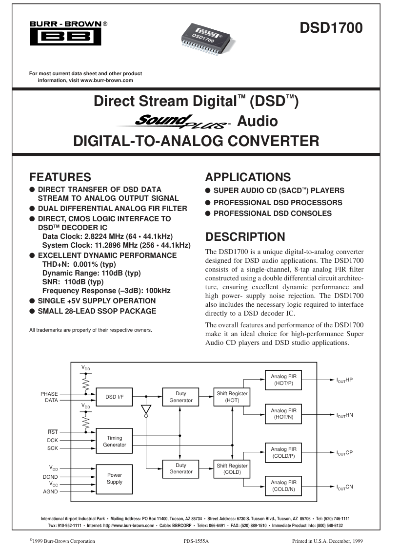
DSD1700 BURR-BROWN
Document overview
- PDF pages: 8
Technical content
Page 1
Page 2
SPECIFICATIONS
All specifications TA = +25°C, VDD = VCC = 5.0V, fS = 44.1kHz, data clock = 64fS, system clock = 256fS, unless otherwise specified. (Although the sampling frequency of Direct Stream Digital is 2.8224MHz, for convenience, in this specification sheet, it is described that the sampling frequency (fS) is 44.1kHz and the 2.8224MHz clock is 64fS).
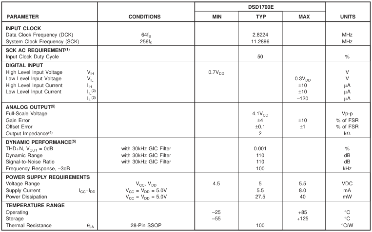
NOTES: (1) See description of system clock in the Functional Description section of this data sheet. (2) Pins 26, 27, 28: DATA. DCK. SCK. (3) Pins 3, 4: RST, PHASE (with internal pull-up). (4) Pins 13, 14, 15, 16: IOUTHN, IOUTCP, IOUTCN, IOUTHP. (5) Measure DSD signal modulated fSIG = 1kHz with 50% scaling factor through standard differential to single-ended converter (see Figure 10) using Audio Precision System II in rms mode with 20kHz LPF and 400Hz HPF.
The information provided herein is believed to be reliable; however, BURR-BROWN assumes no responsibility for inaccuracies or omissions. BURR-BROWN assumes no responsibility for the use of this information, and all use of such information shall be entirely at the user’s own risk. Prices and specifications are subject to change without notice. No patent rights or licenses to any of the circuits described herein are implied or granted to any third party. BURR-BROWN does not authorize or warrant any BURR-BROWN product for use in life support devices and/or systems.
Page 3
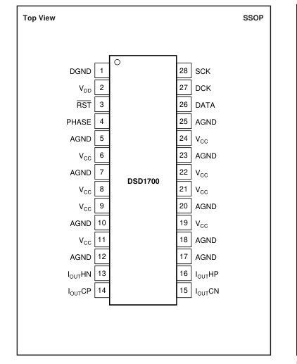
PIN CONFIGURATION
ABSOLUTE MAXIMUM RATINGS(1)
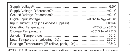
NOTE: (1) Stresses above these ratings may cause permanent damage. Exposure to absolute maximum conditions for extended periods may degrade device reliability. (2) VCC, VDD. (3) Among VCC, VDD. (4) Among AGND, DGND.
PACKAGE/ORDERING INFORMATION
PIN ASSIGNMENTS
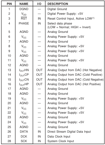
NOTE: (1) With internal pull-up resistor
ELECTROSTATIC
DISCHARGE SENSITIVITY
This integrated circuit can be damaged by ESD. Burr-Brown
recommends that all integrated circuits be handled with
appropriate precautions. Failure to observe proper handling
and installation procedures can cause damage. ESD damage can range from subtle performance degrada-
tion to complete device failure. Precision integrated circuits
may be more susceptible to damage because very small
parametric changes could cause the device not to meet its
published specifications.
| PRODUCT | PACKAGE | PACKAGE DRAWING NUMBER | SPECIFIED TEMPERATURE RANGE | PACKAGE MARKING | ORDERING NUMBER(1) | TRANSPORT MEDIA |
| DSD1700E " | 28-Lead SSOP " | 324 " | 0°C to +70°C " | DSD1700E " | DSD1700E DSD1700E/2K | Rails Tape and Reel |
NOTE: (1) Models with a slash (/) are available only in Tape and Reel in the quantities indicated (e.g., /2K indicates 2000 devices per reel). Ordering 2000 pieces of “DSD1700E/2K” will get a single 2000-piece Tape and Reel.
Page 4
GENERAL INFORMATION
The DSD1700 is designed solely for use in DSD and SACD applications. It is not compatible with standard CD audio transports, or DVD/MPEG-2 decoders. Burr-Brown manufacturers a wide array of products for these applications. Please refer to our audio brochure and product data sheets, available from our web site (www.burr-brown.com) and local sales offices.
FUNCTIONAL DESCRIPTION
The concept of Direct Stream Digital (DSD) conversion is simple. An analog audio input is digitized by a 1-bit, 64x oversampled delta-sigma modulator. The 1-bit data stream is then stored and may be transferred to a SACD disc at a later time. For playback, the 1-bit, 64x oversampled data is then presented to the DSD1700 directly by a DSD decoder IC. The DSD1700 then low-pass filters the oversampled data to reconstruct the original analog audio waveform. The recording and playback functions are illustrated in Figures 1 and 2 respectively. To perform the digital-to-analog conversion, the DSD1700 includes both the decoder interface logic and an analog FIR filter. The following paragraphs provide a summary of these
functions.
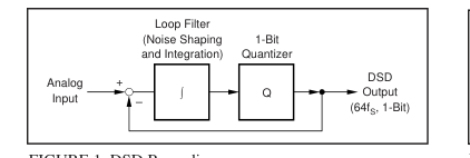
FIGURE 1. DSD Recording.
DECODER INTERFACE
The decoder interface consists of several CMOS logic in- puts. The system clock input, SCK (pin 28), operates at 11.2896MHz (256 • 44.1kHz). The data bit clock, DCK (pin 27), operates at 2.8244 MHz (64 • 44.1kHz) and is the 64x oversampled data clock. The 1-bit, 64x oversampled data stream is input at DATA (pin 26). DATA and DCK are synchronized to the SCK falling edge. The DSD1700 generates HOT and COLD data internally for use with the double differential analog FIR filter. The PHASE input (pin 4) is used to determine the polarity of the HOT and COLD data (normal or inverted). The PHASE input is synchronized to the rising edge of SCK.
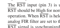
The RST input (pin 3) is used for system reset purposes. RST should be High for normal operation, and Low for reset operation. When RST is held Low, the current outputs of the analog FIR filter are set to the bipolar zero (BPZ) level. The RST signal is synchronized to the rising edge of SCK.
TIMING
Figures 3 though 6 show the timing diagrams for the DSD1700 interface signals. Figure 3 shows the system clock (SCK) timing requirements. Figure 4 shows the general timing for the data input. Figures 5 and 6 show the detailed timing for the DSD data and control data inputs.
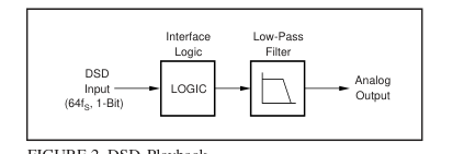
FIGURE 2. DSD Playback.


FIGURE 3. System Clock Timing.
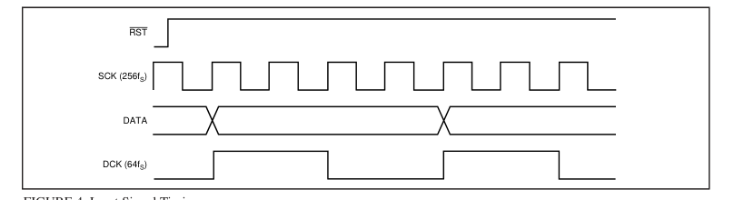
FIGURE 4. Input Signal Timing.
Page 5
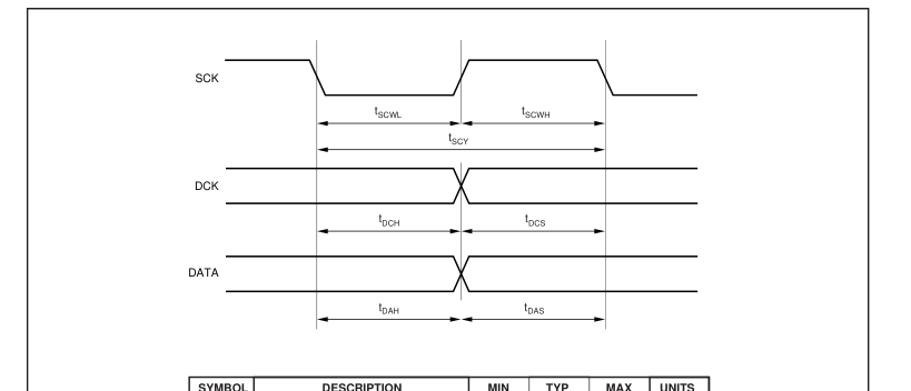
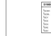
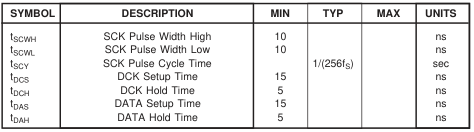
FIGURE 5. DSD Data Input Timing.
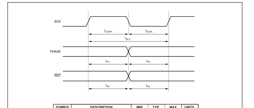
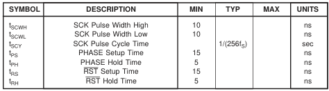
FIGURE 6. Control Data Input Timing.
Page 6
ANALOG FIR FILTER The low-pass filter function for the DSD1700 is constructed
by using four 8-tap, analog FIR filters with current outputs.
The four filters include one each for HOT and COLD
positive, and one each for HOT and COLD negative. This is
referred to as a double differential architecture. These filters
use resistors to set the filter coefficients, as shown in
Figure 7. Prior to the analog FIR filters, the duty cycle of the
DSD input signal is set to 75% by the DSD1700’s duty
generators. Plots of the analog FIR filter response is shown in Figure 8.
The stop-band attenuation of the filters dictates that addi-
tional low-pass filtering is required at the output of the
external current-to-voltage converter circuit (see Figure 10).
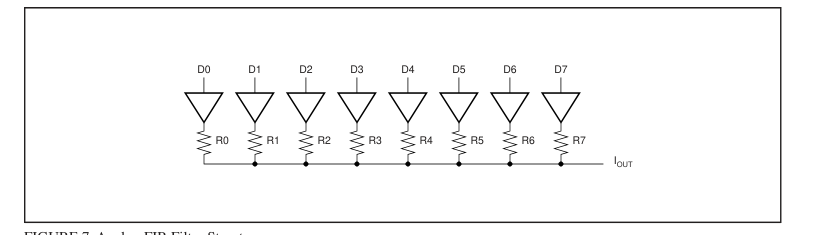
FIGURE 7. Analog FIR Filter Structure.
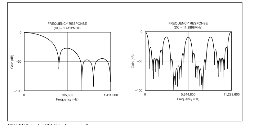
FIGURE 8. Analog FIR Filter Frequency Response.
Page 7
APPLICATIONS INFORMATION
TYPICAL CONNECTIONS
Figure 9 shows the basic connection diagram for the DSD1700. A significant number of power supply bypass capacitors are required, and Burr-Brown recommends the indicated values for optimal performance.
CURRENT-TO-VOLTAGE (I/V)
CONVERTER CIRCUIT
The DSD1700 is a current output device, and requires an I/V conversion circuit to transform the double-differential outputs into a usable voltage output. The circuit in Figure 10 is recommended for this purpose. Op amps are OPA134 or equivalent.
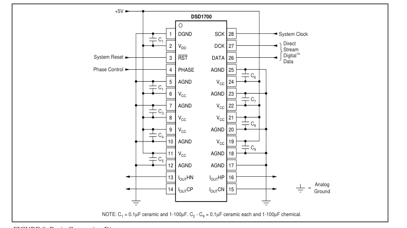
FIGURE 9. Basic Connection Diagram.
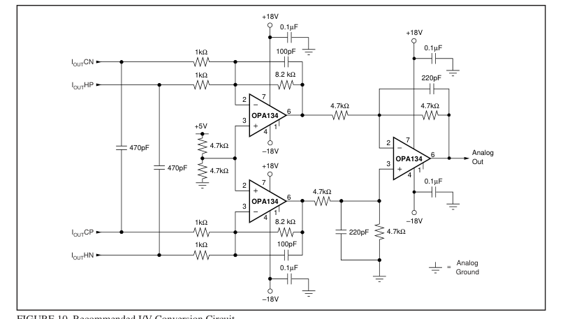
FIGURE 10. Recommended I/V Conversion Circuit.
Page 8
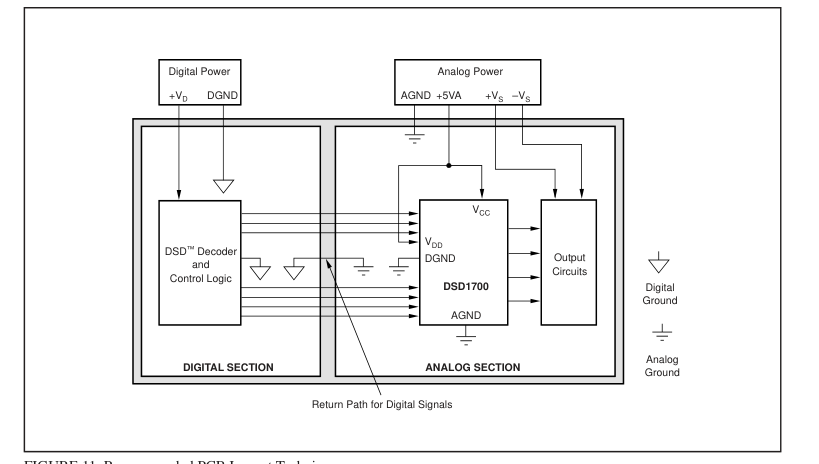
PRINTED CIRCUIT BOARD LAYOUT A typical PCB floor plan for the DSD1700 is shown in
Figure 11. A ground plane is recommended, with the analog
and digital sections being isolated from one another using a
split in the plane. The DSD1700 should be oriented with the
digital I/O pins facing the ground plane split/cut, allowing
for direct connection to the DSD decoder and control signals
originating from the digital section of the board.
Separate power supplies are recommended for the digital
and analog sections of the board. This prevents the switching
noise present on the digital supply from contaminating the
analog power supply and degrading the dynamic perfor-
mance of the DSD1700.